Issue Browser
Volume 44, Issue 12,
Dec 2023

J. Semicond.
2023, 44(12): 121401 doi: 10.1088/1674-4926/44/12/121401
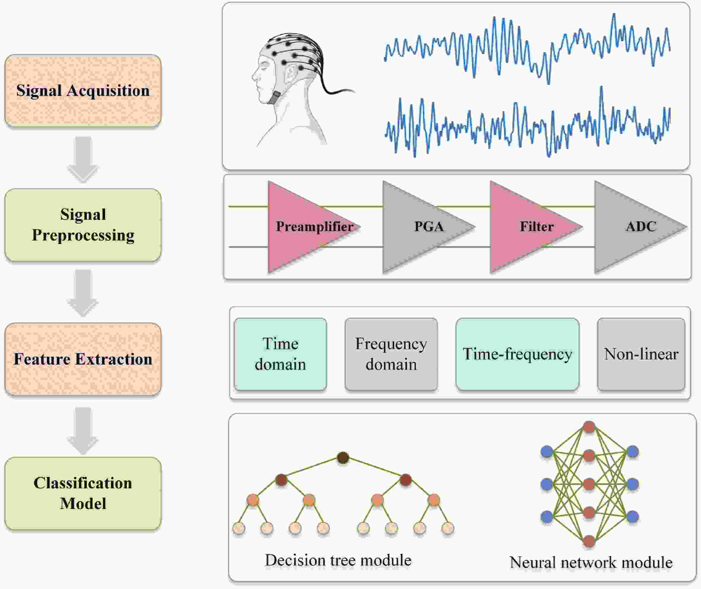
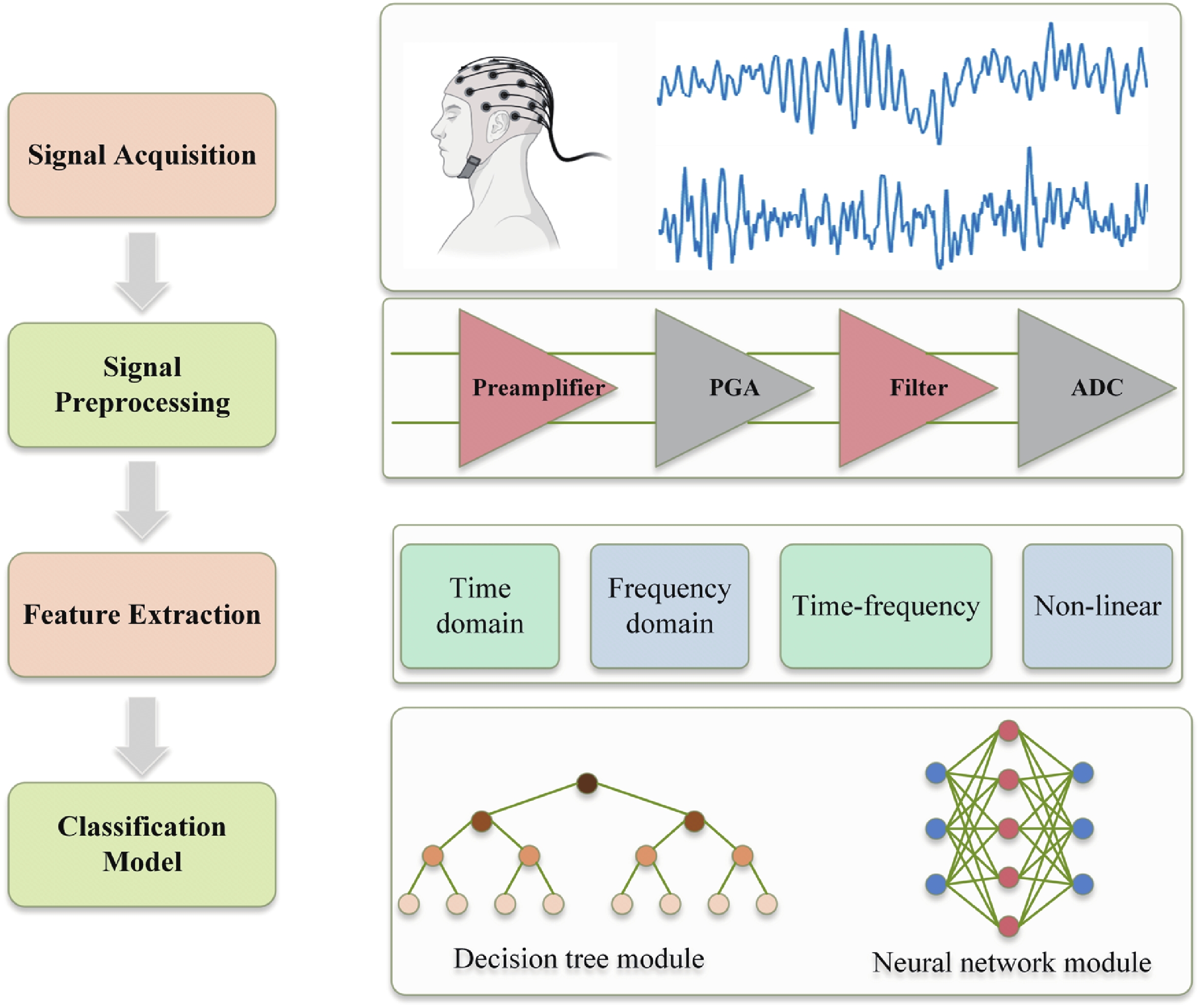
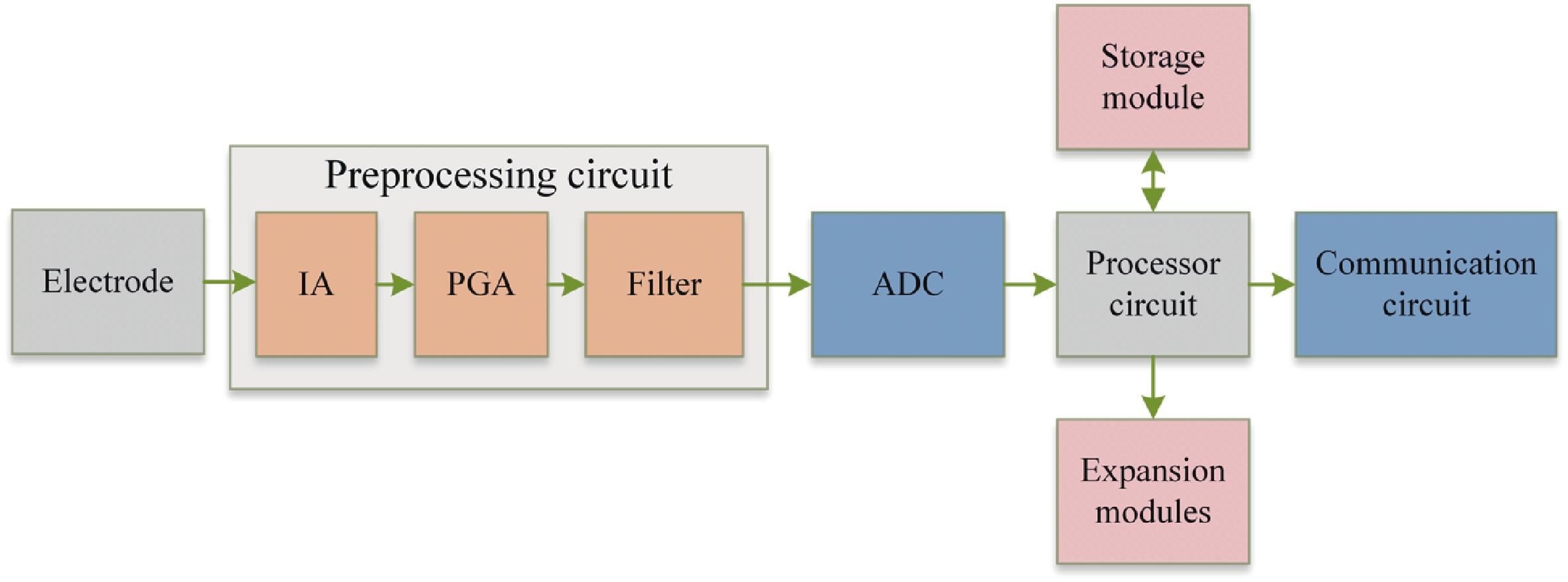
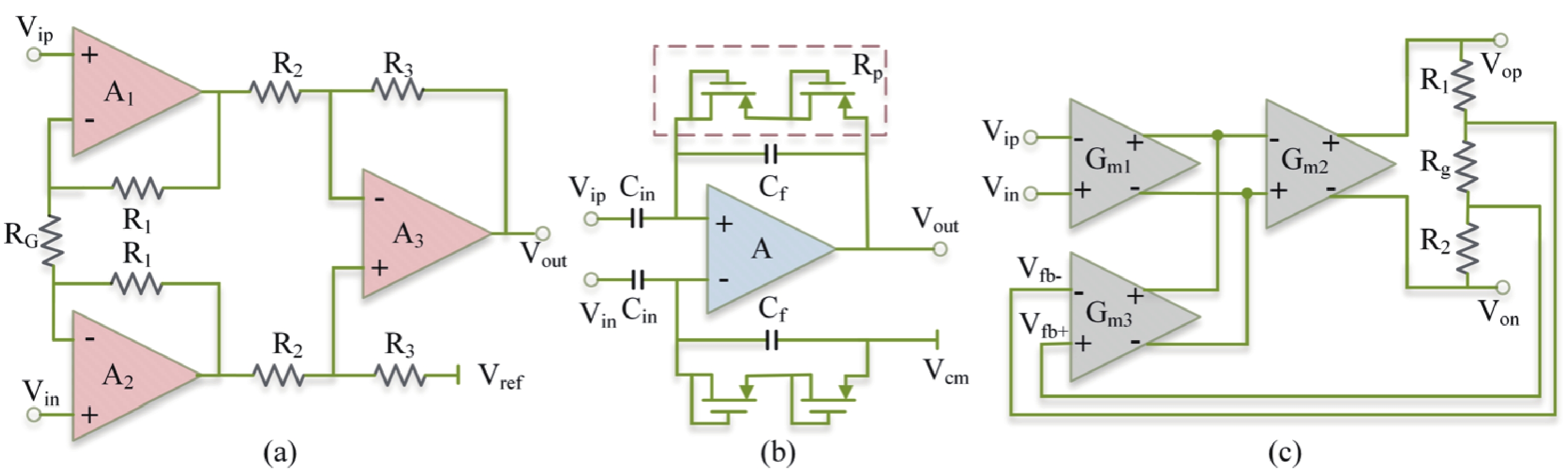
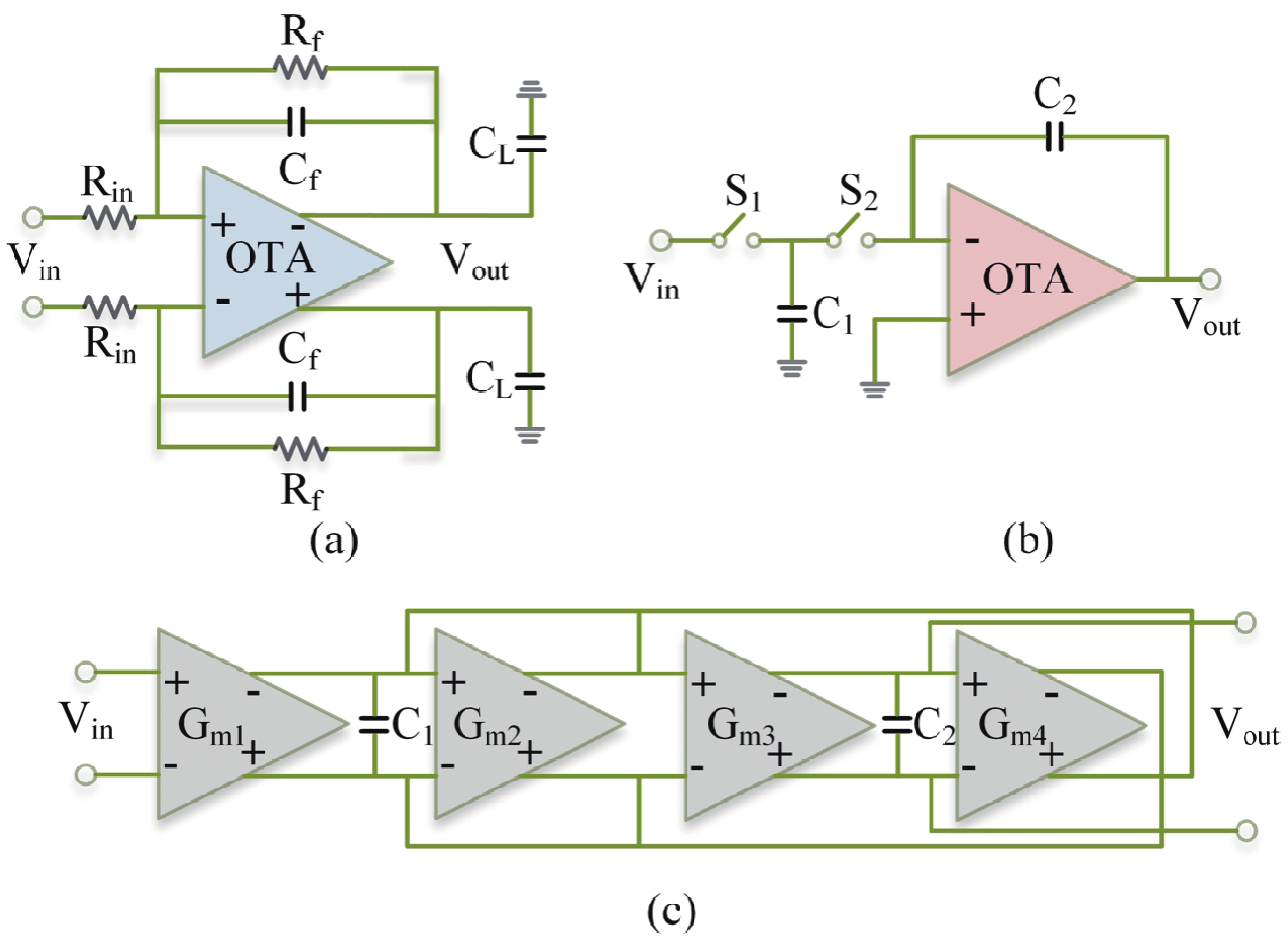
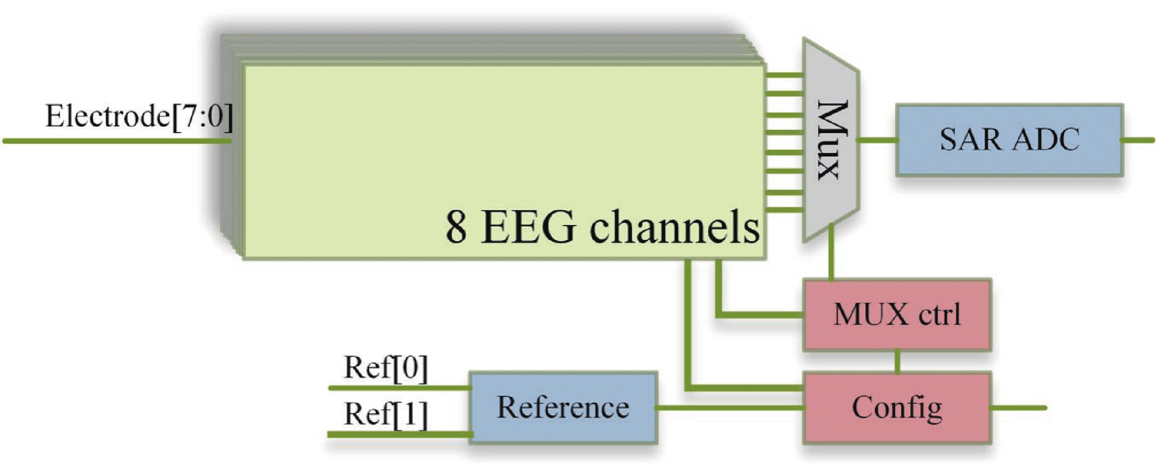
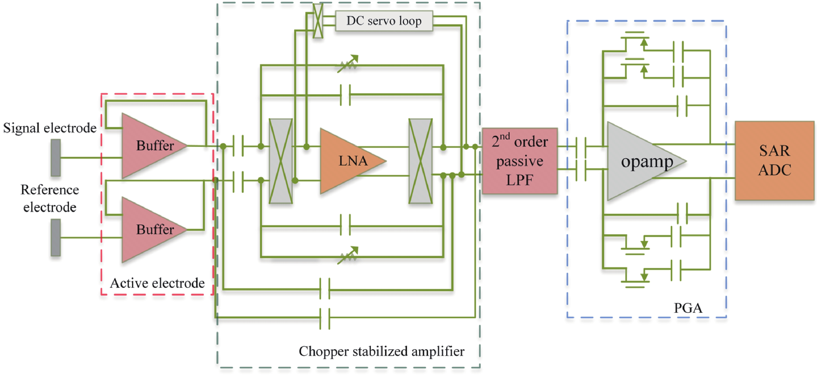
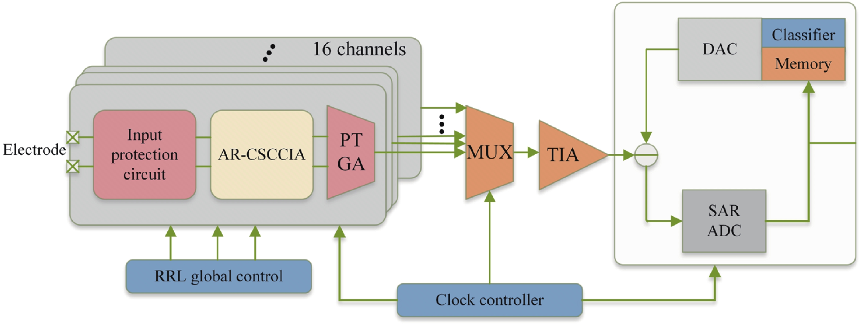
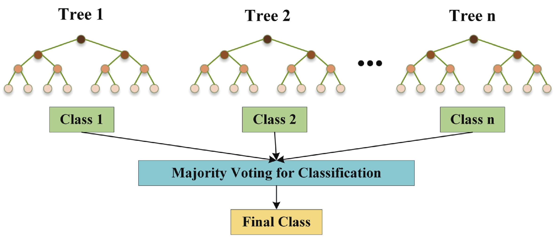
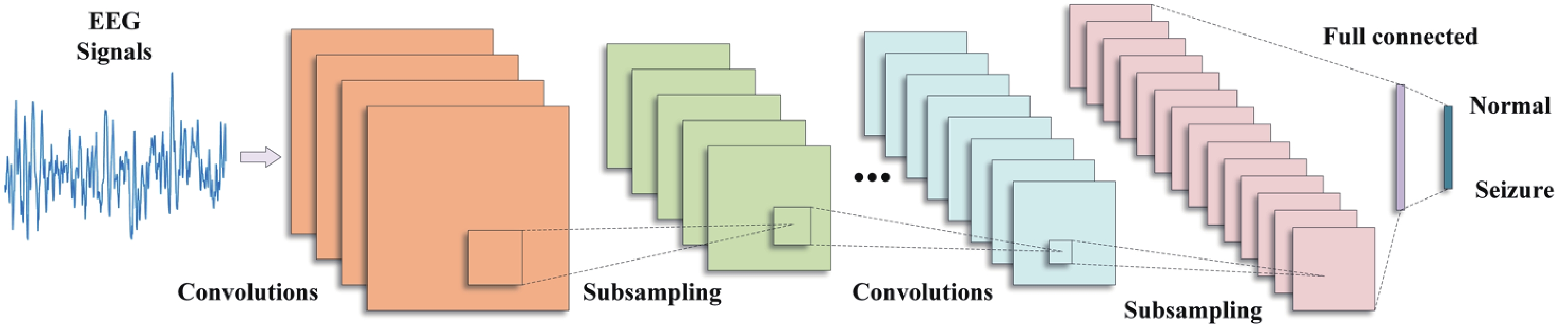
Epilepsy is a common neurological disorder that occurs at all ages. Epilepsy not only brings physical pain to patients, but also brings a huge burden to the lives of patients and their families. At present, epilepsy detection is still achieved through the observation of electroencephalography (EEG) by medical staff. However, this process takes a long time and consumes energy, which will create a huge workload to medical staff. Therefore, it is particularly important to realize the automatic detection of epilepsy. This paper introduces, in detail, the overall framework of EEG-based automatic epilepsy identification and the typical methods involved in each step. Aiming at the core modules, that is, signal acquisition analog front end (AFE), feature extraction and classifier selection, method summary and theoretical explanation are carried out. Finally, the future research directions in the field of automatic detection of epilepsy are prospected.

J. Semicond.
2023, 44(12): 121801 doi: 10.1088/1674-4926/44/12/121801

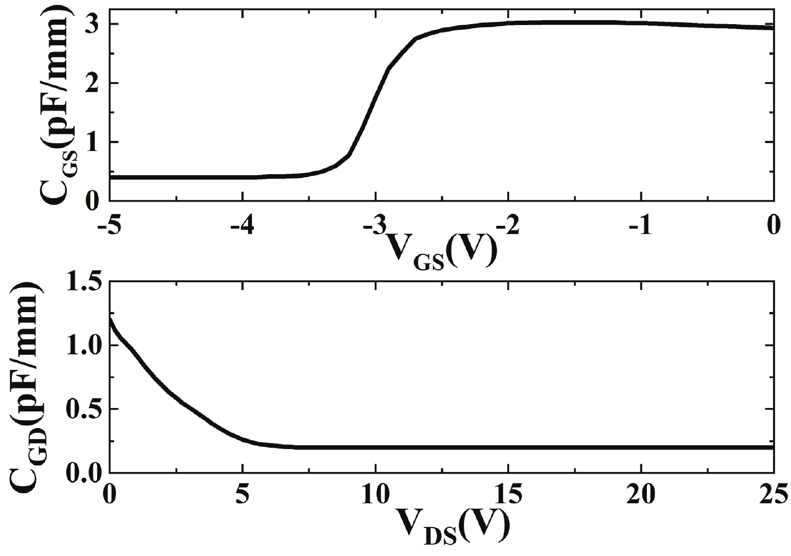
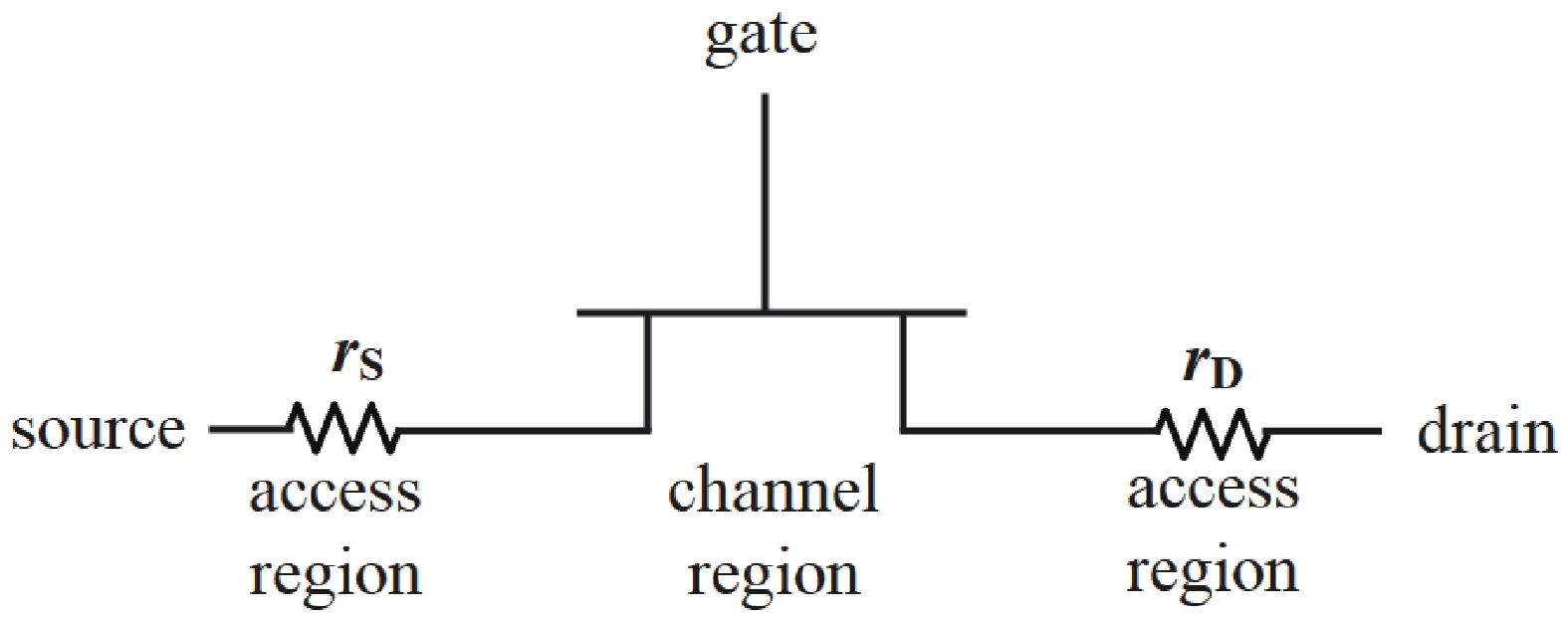
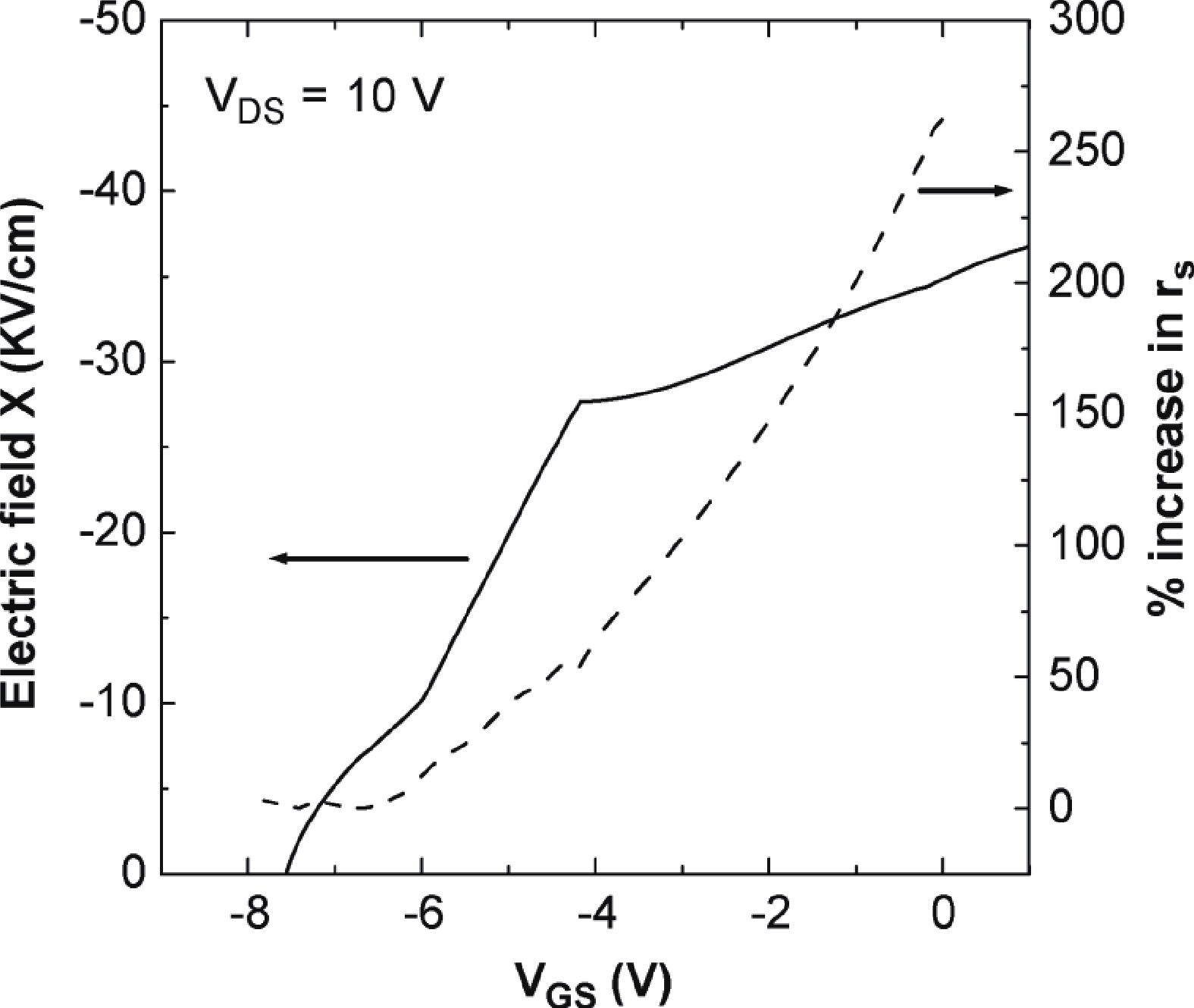
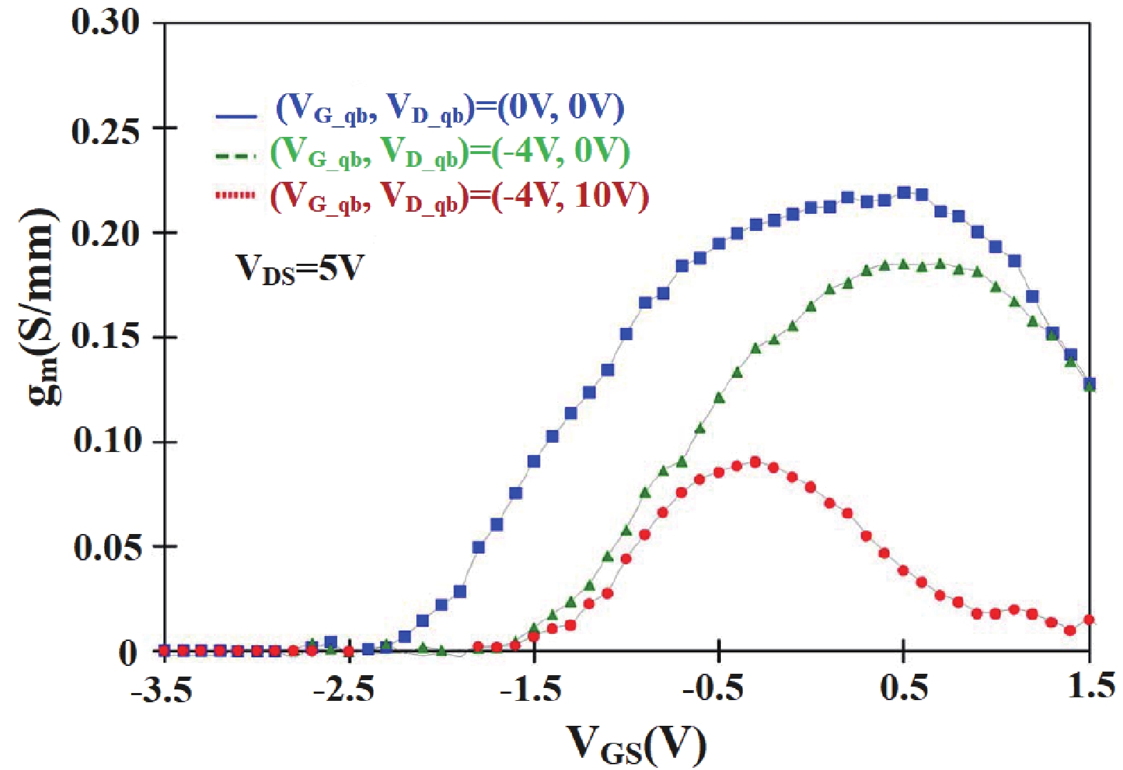
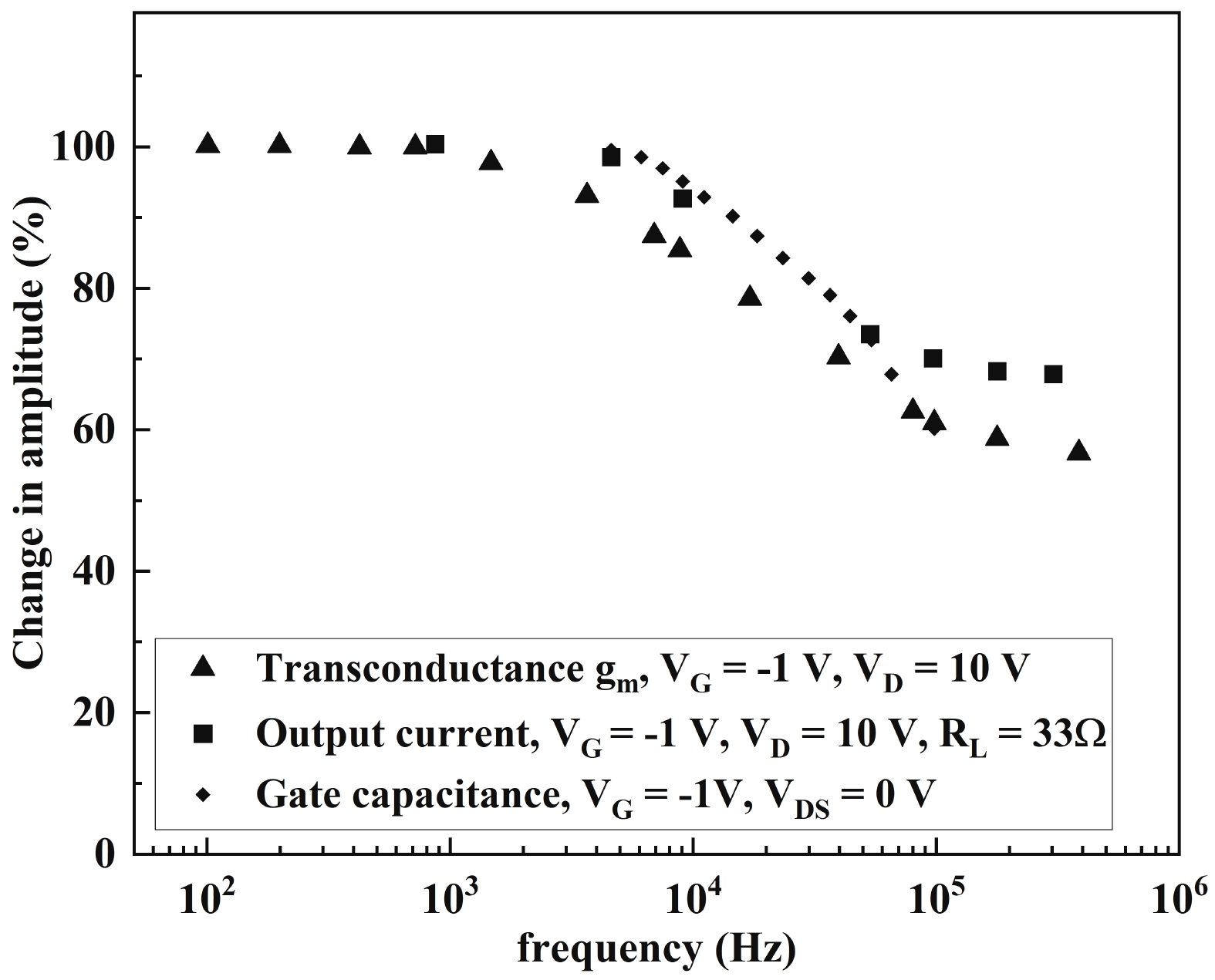
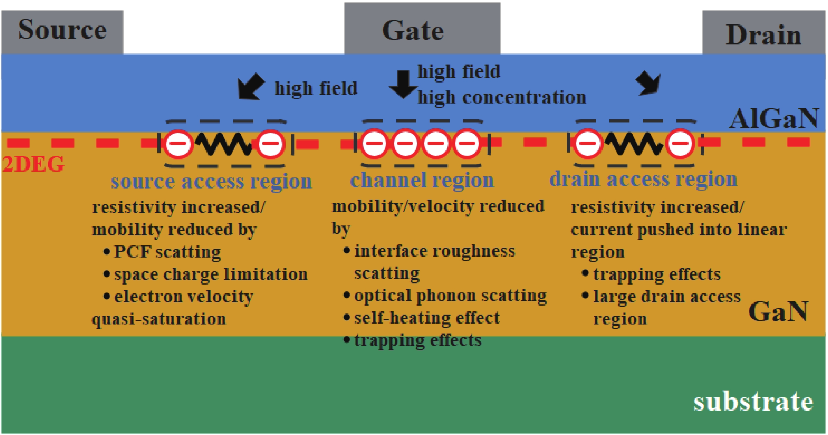
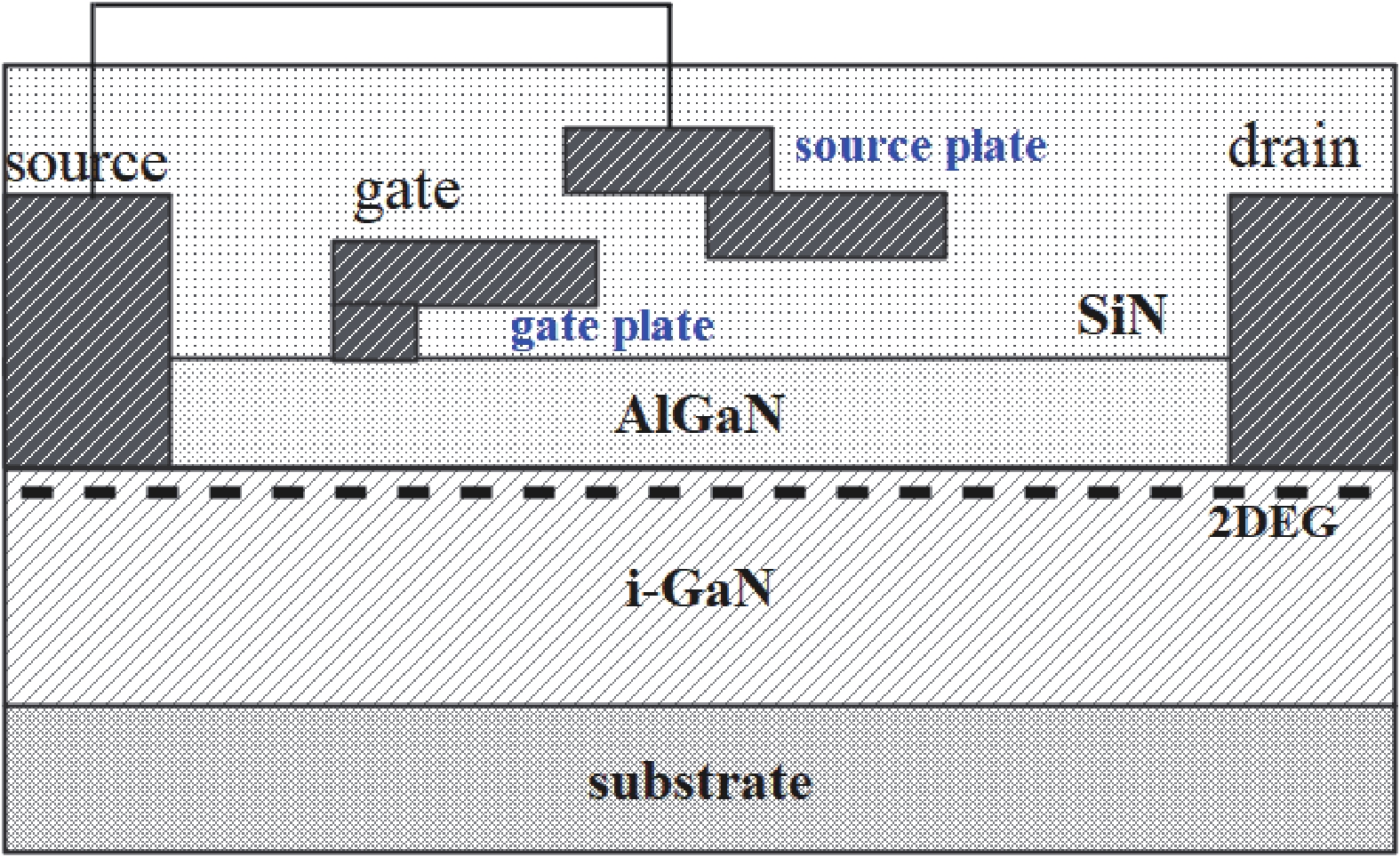
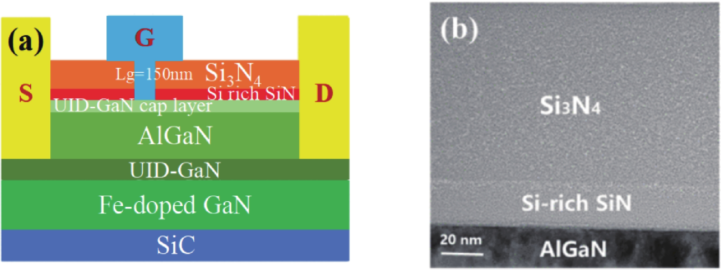
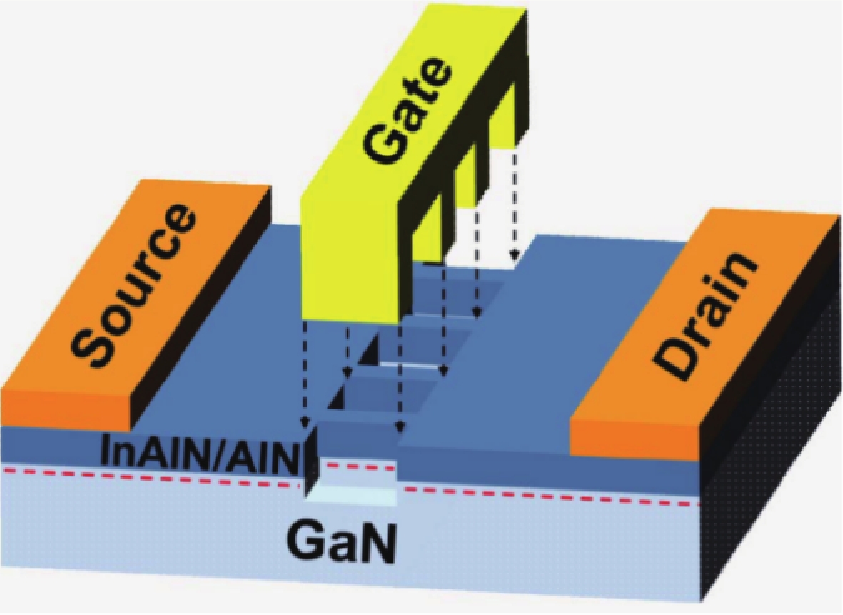
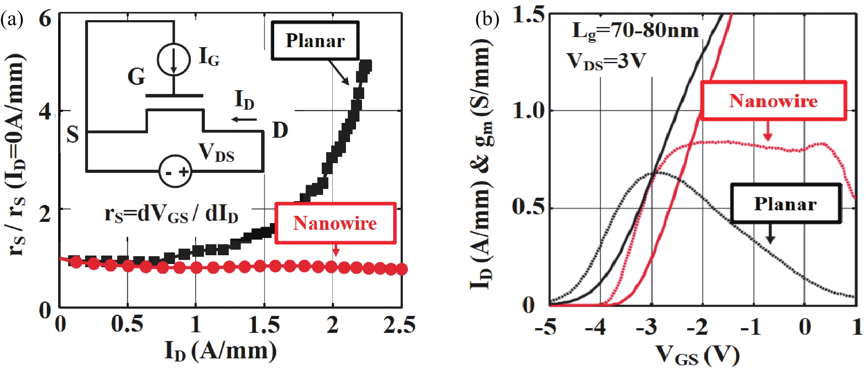
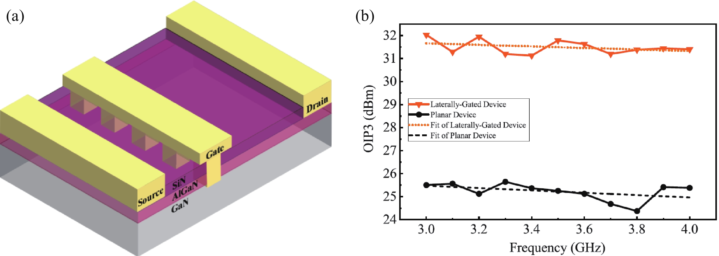
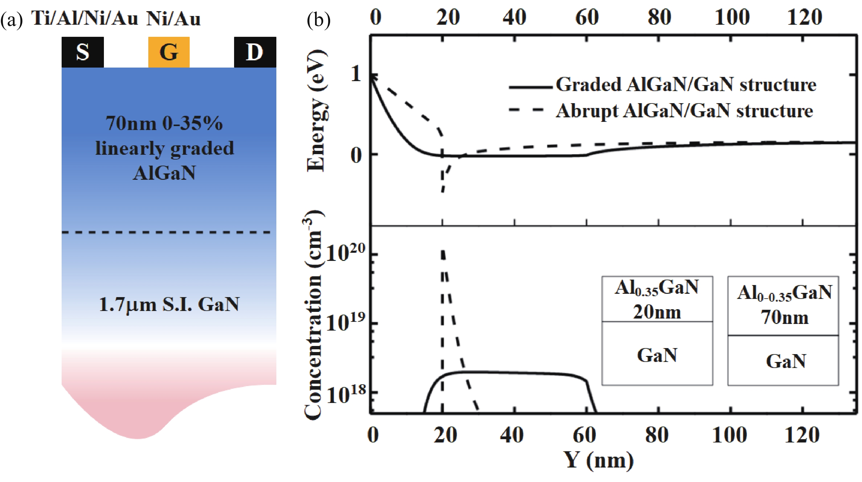
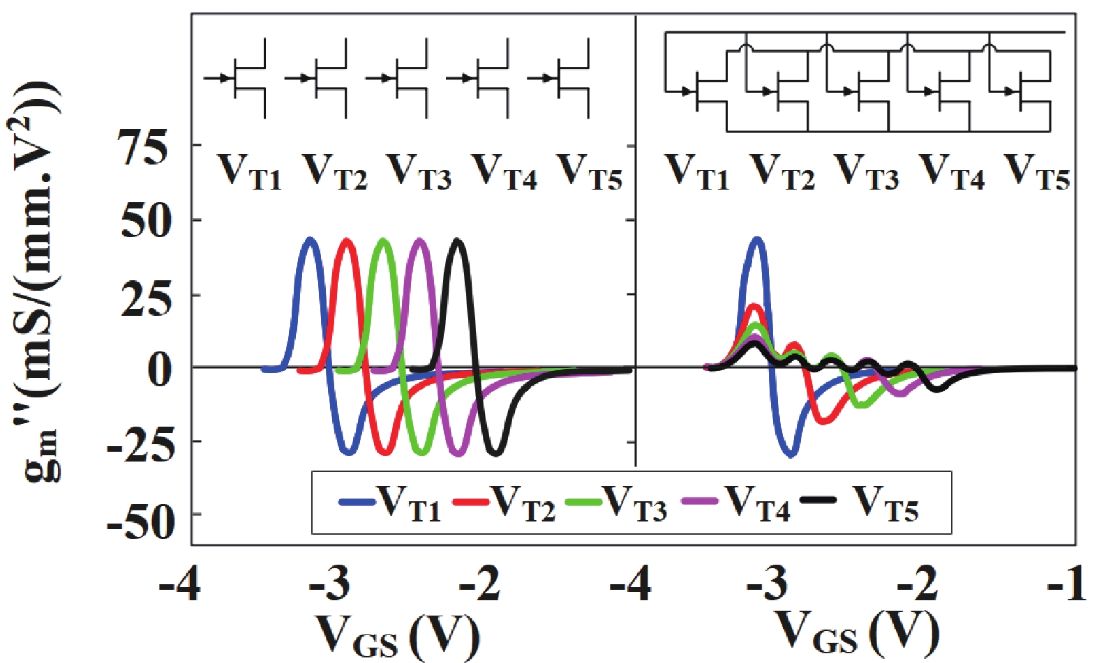
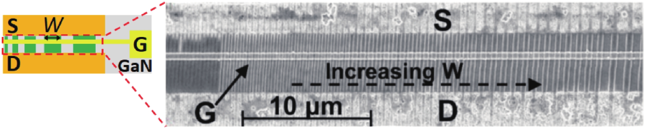
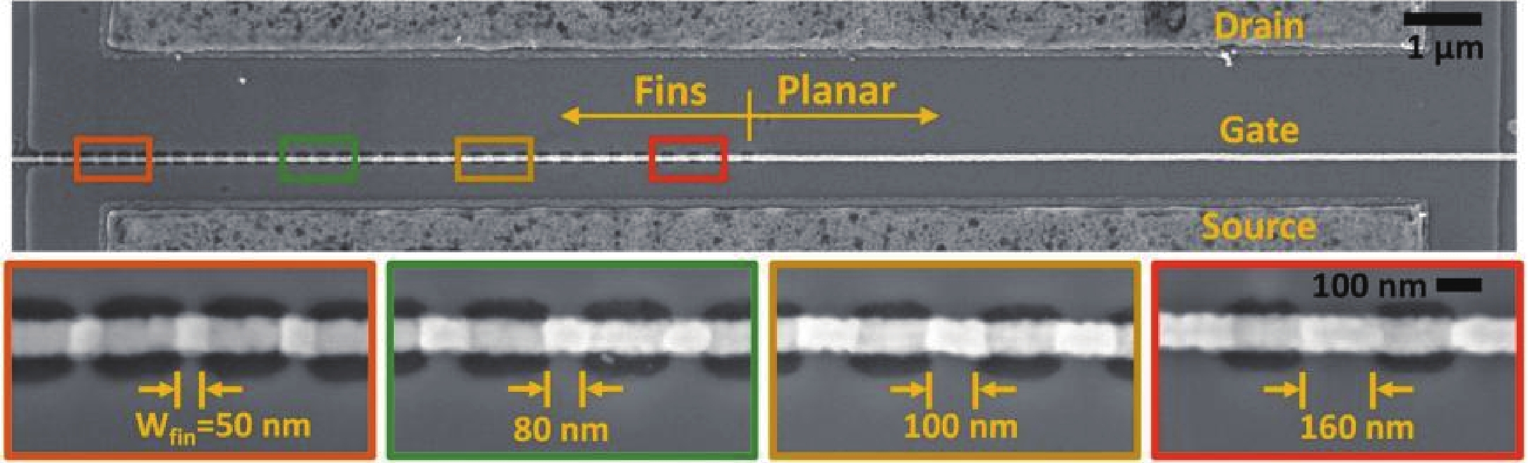
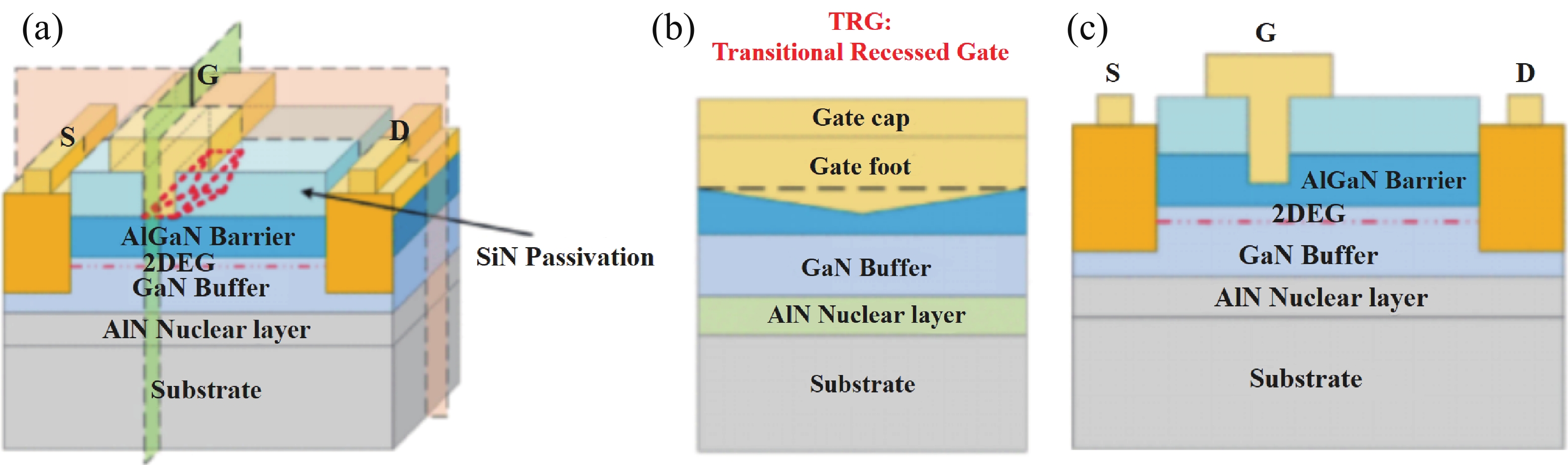
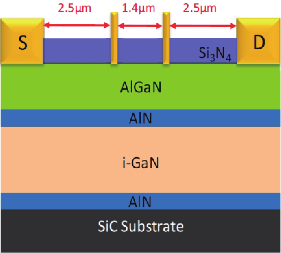
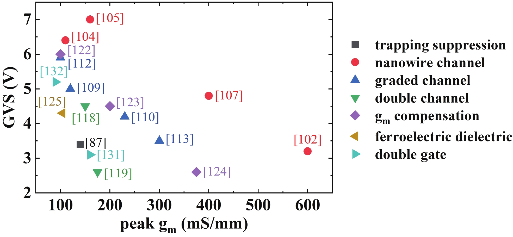
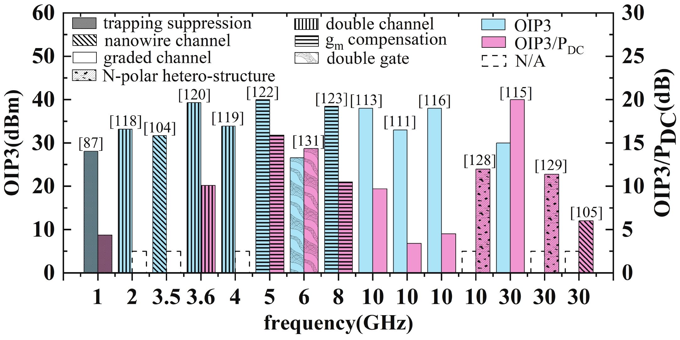
The GaN HEMT is a potential candidate for RF applications due to the high frequency and large power handling capability. To ensure the quality of the communication signal, linearity is a key parameter during the system design. However, the GaN HEMT usually suffers from the nonlinearity problems induced by the nonlinear parasitic capacitance, transconductance, channel transconductance etc. Among them, the transconductance reduction is the main contributor for the nonlinearity and is mostly attributed to the scattering effect, the increasing resistance of access region, the self-heating effect and the trapping effects. Based on the mechanisms, device-level improvement methods of transconductance including the trapping suppression, the nanowire channel, the graded channel, the double channel, the transconductance compensation and the new material structures have been proposed recently. The features of each method are reviewed and compared to provide an overview perspective on the linearity of the GaN HEMT at the device level.


J. Semicond.
2023, 44(12): 121901 doi: 10.1088/1674-4926/44/12/121901
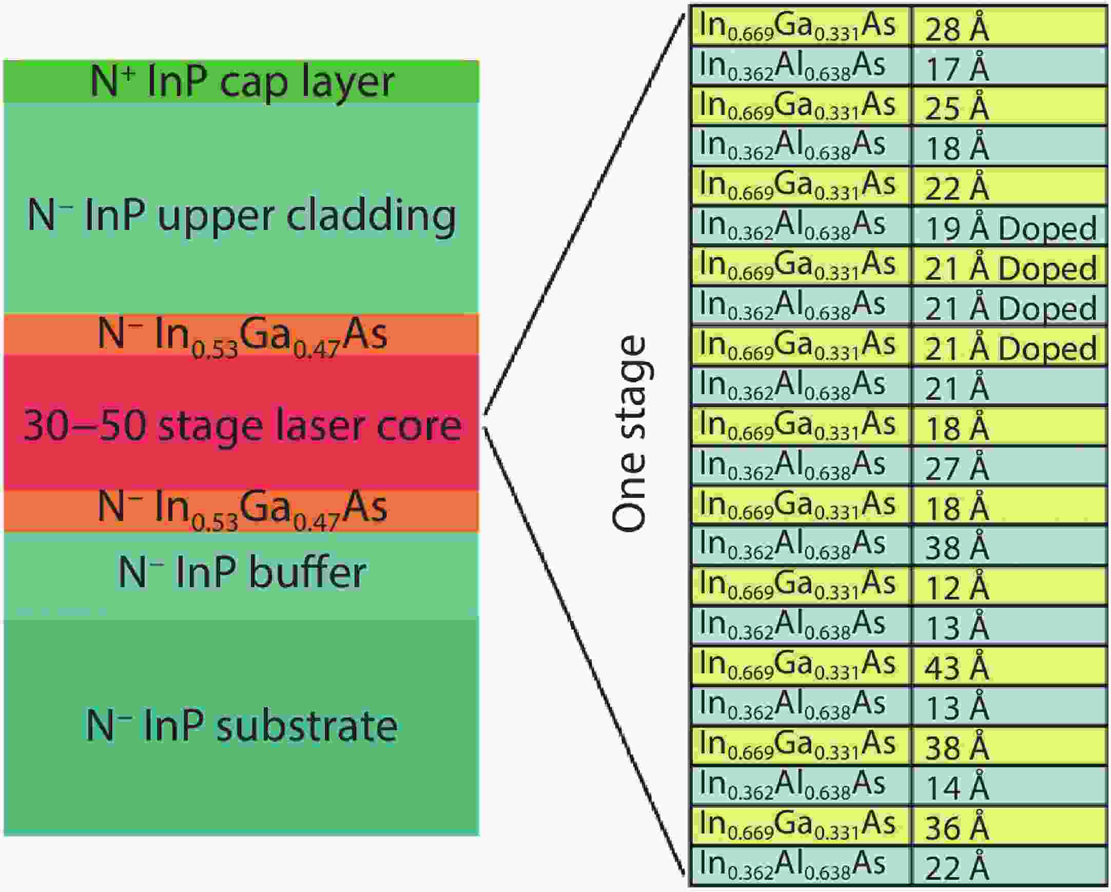
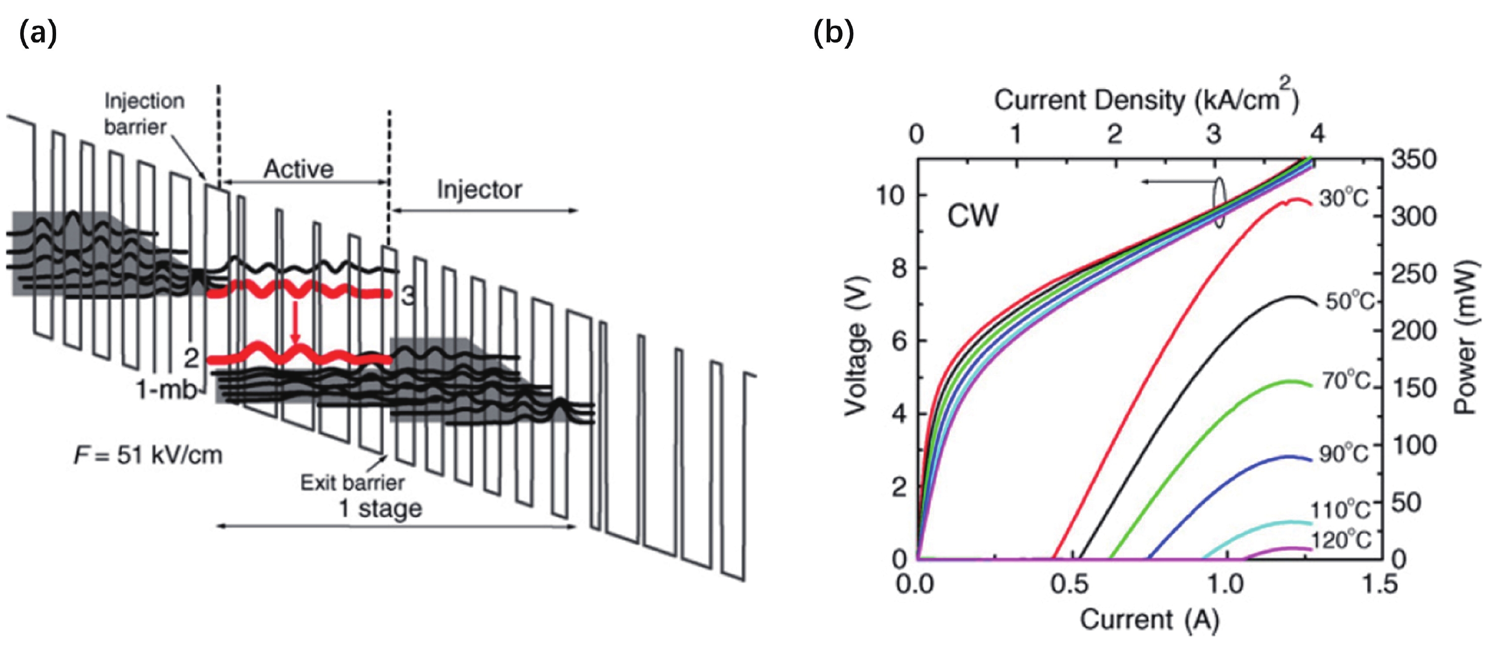
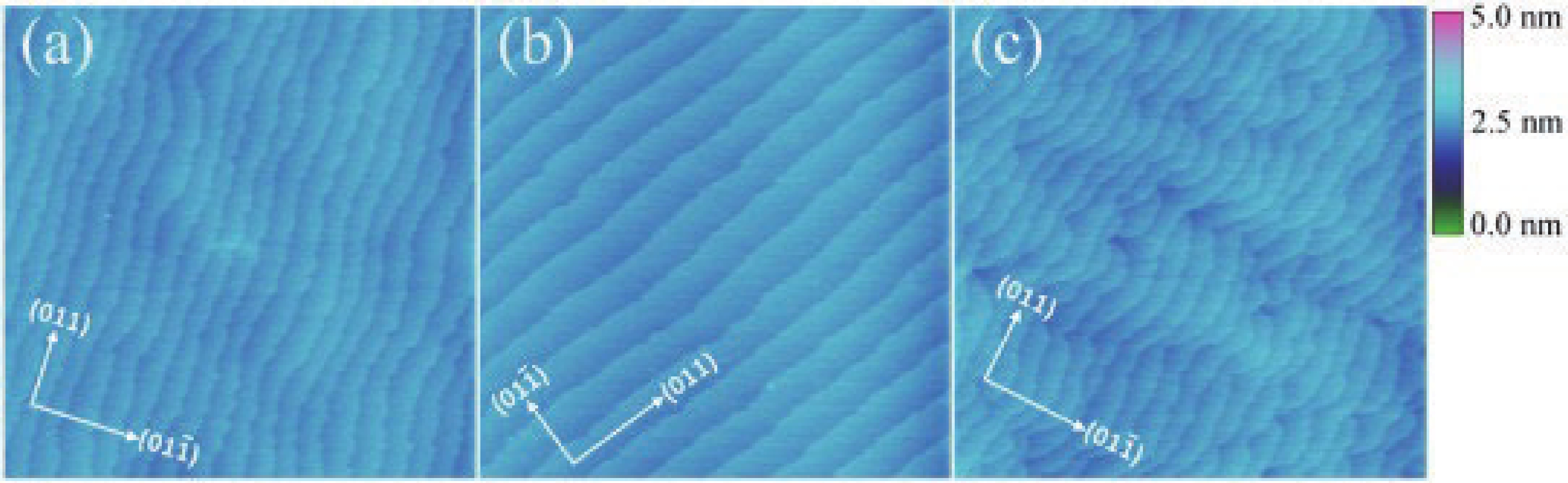
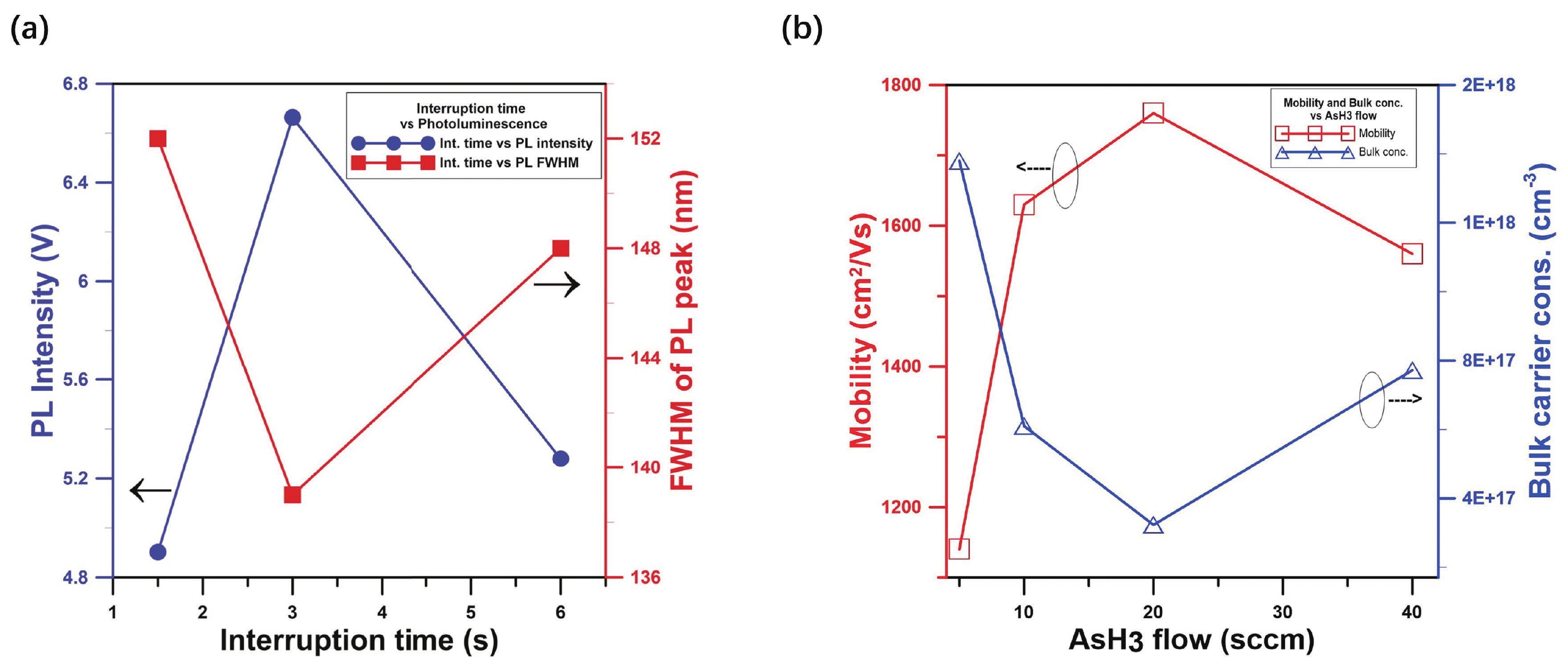
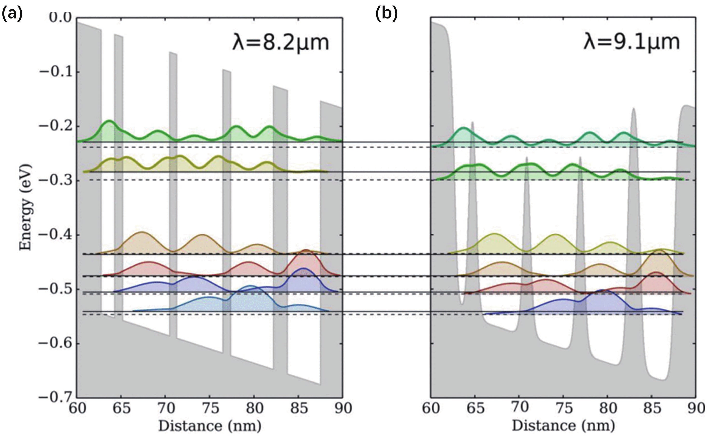
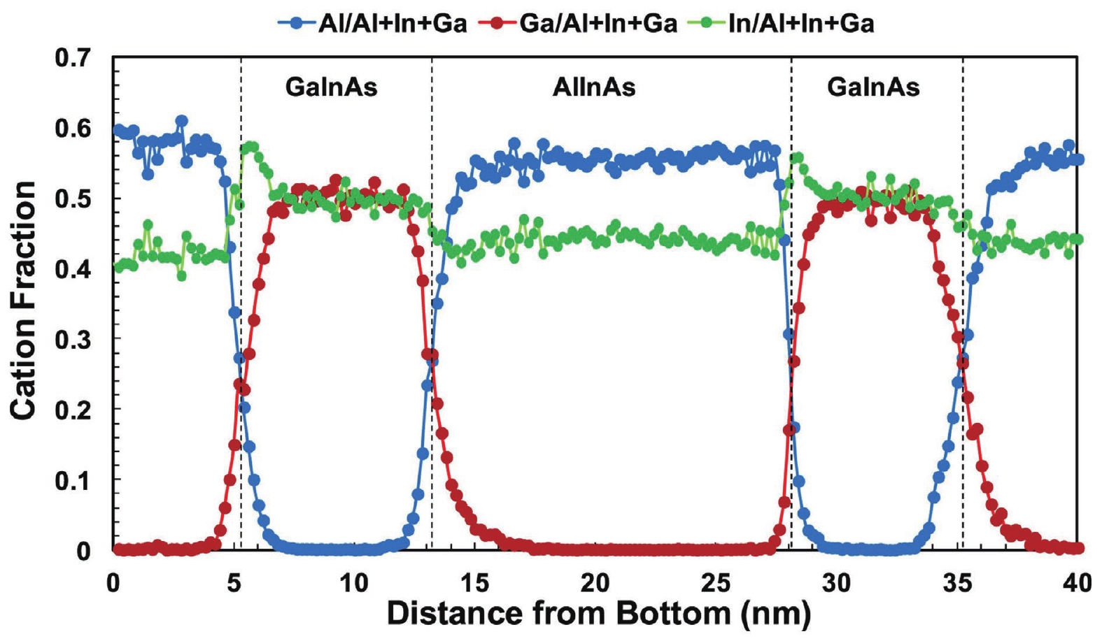
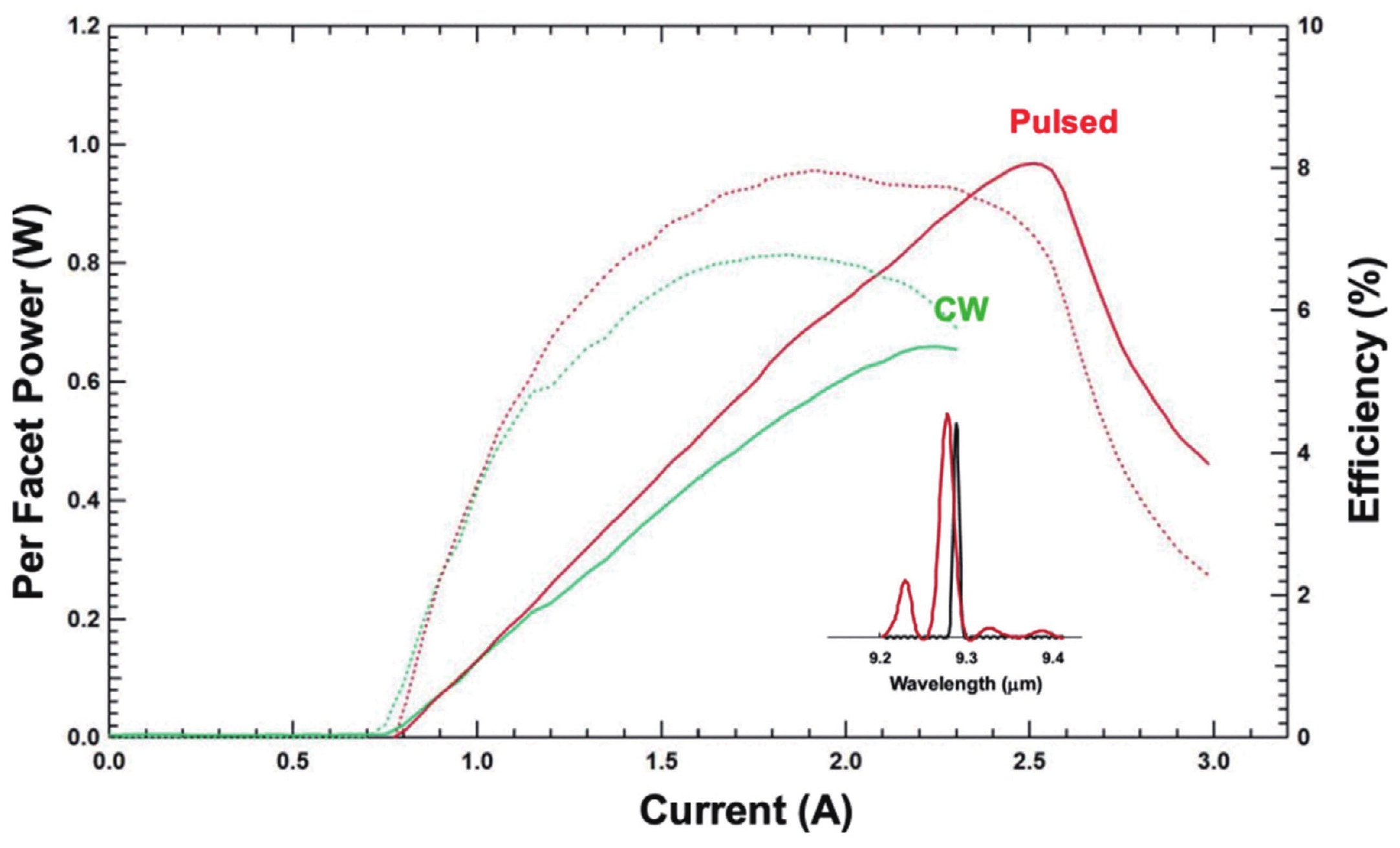
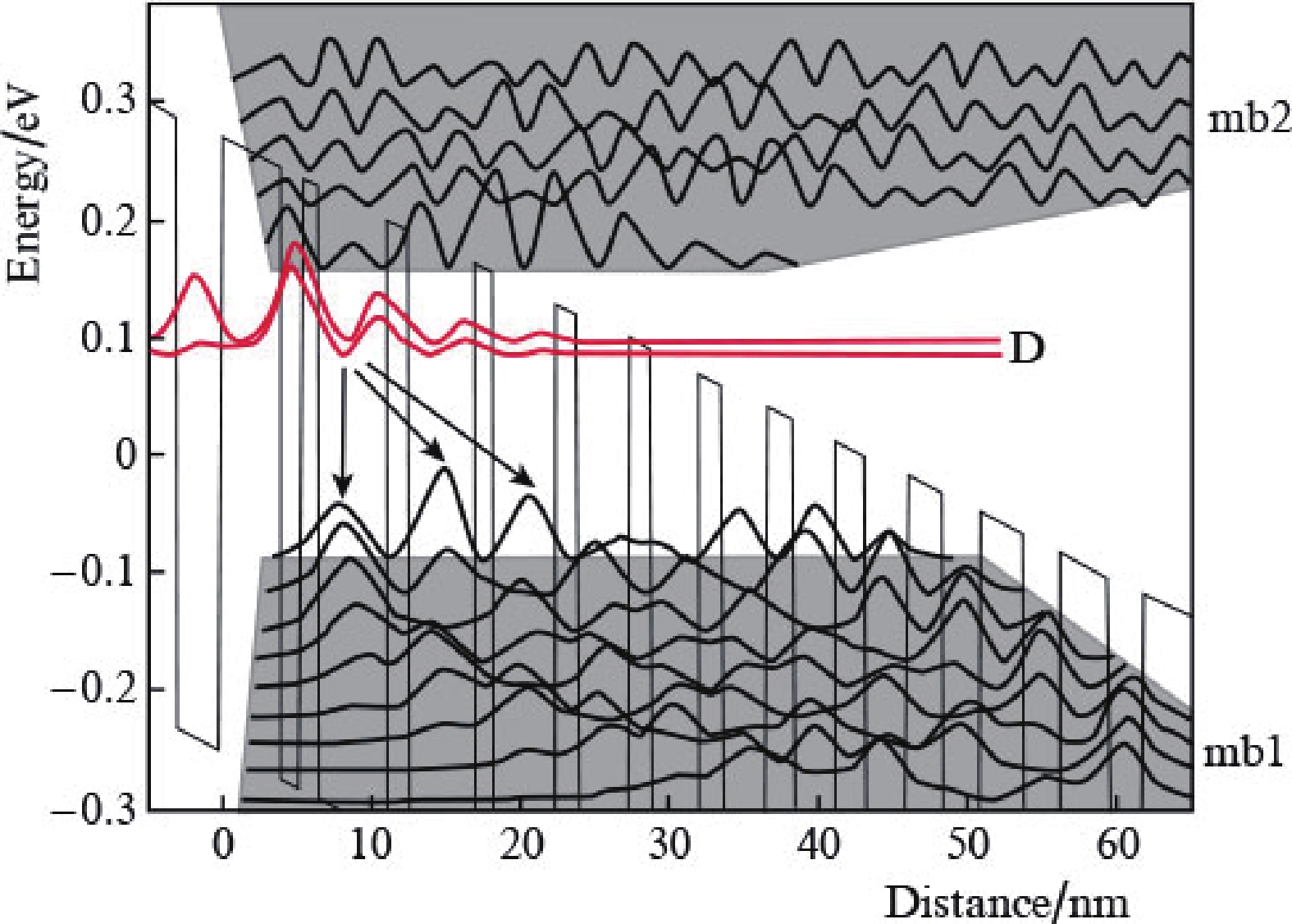
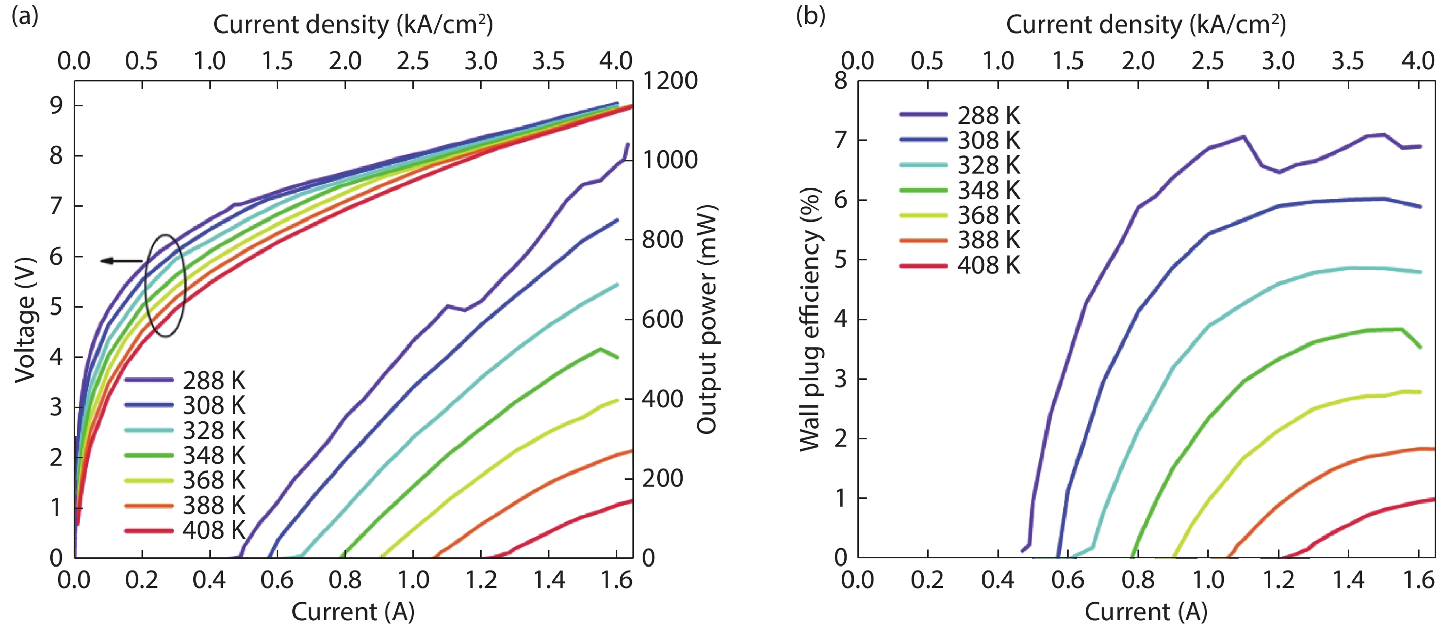
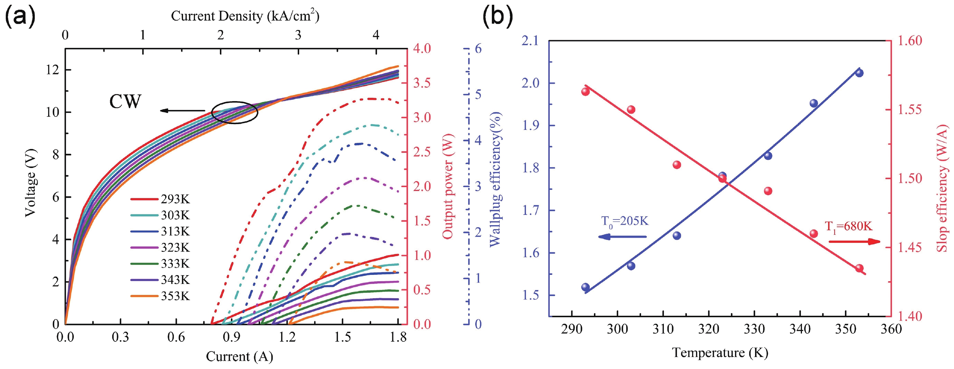
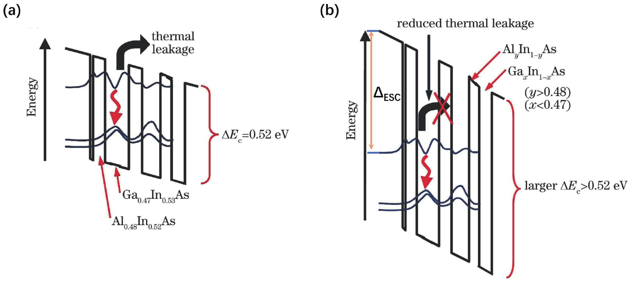
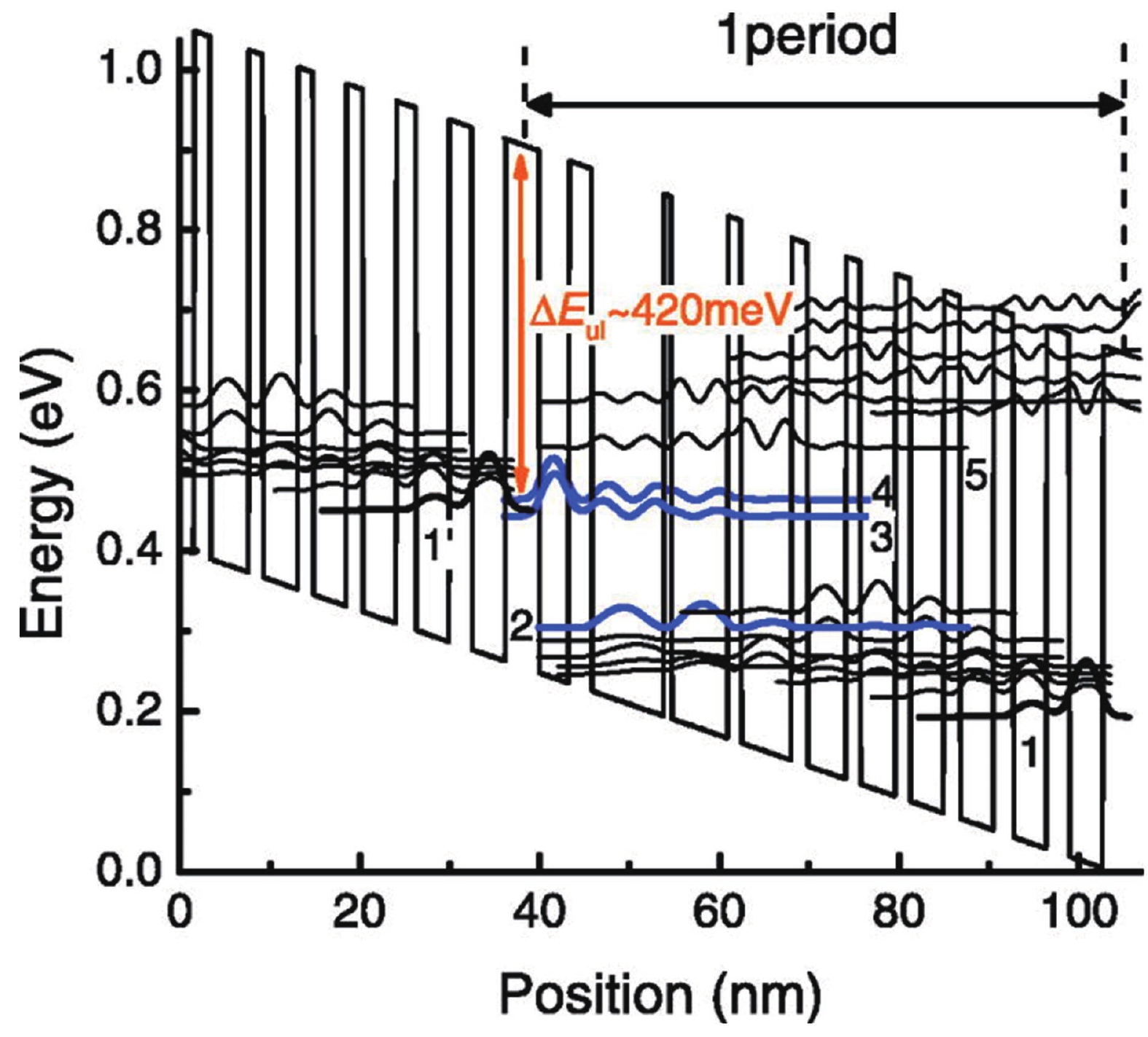
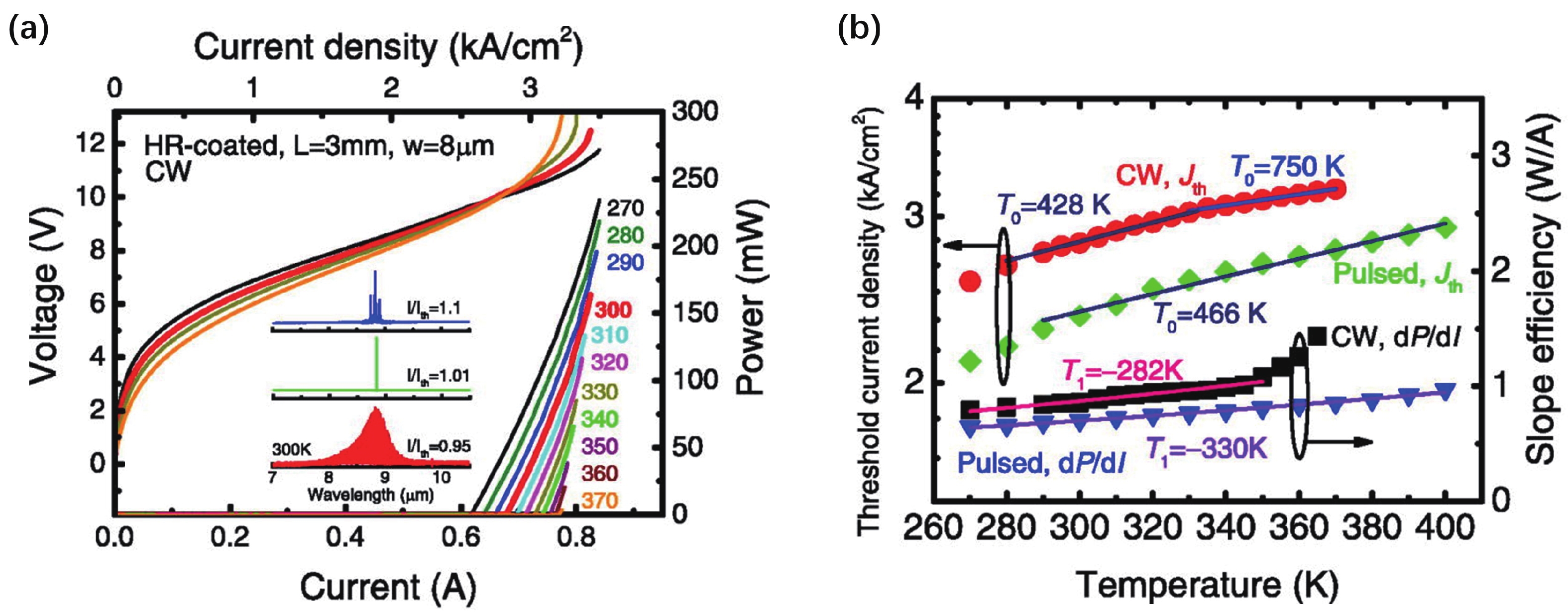
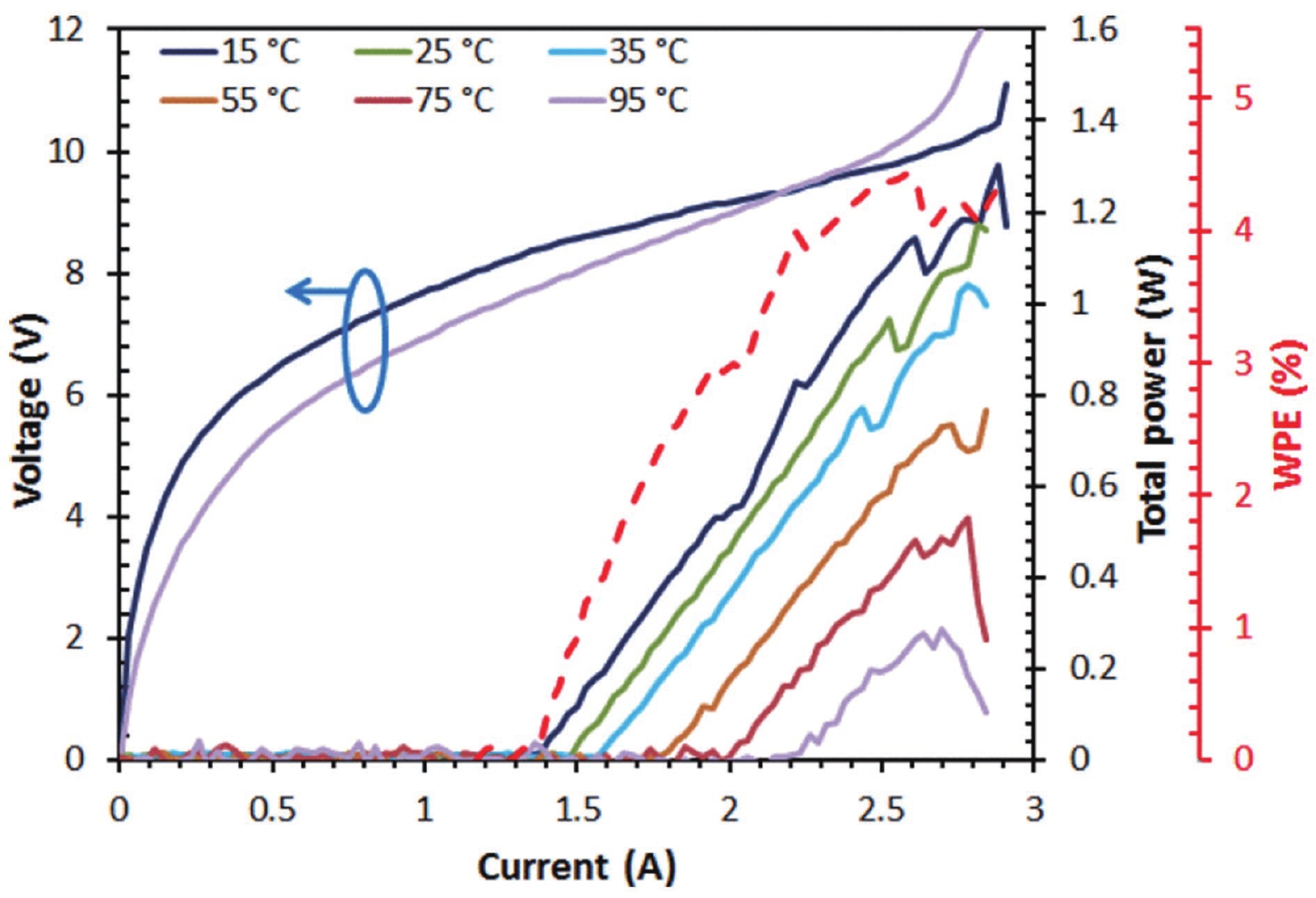
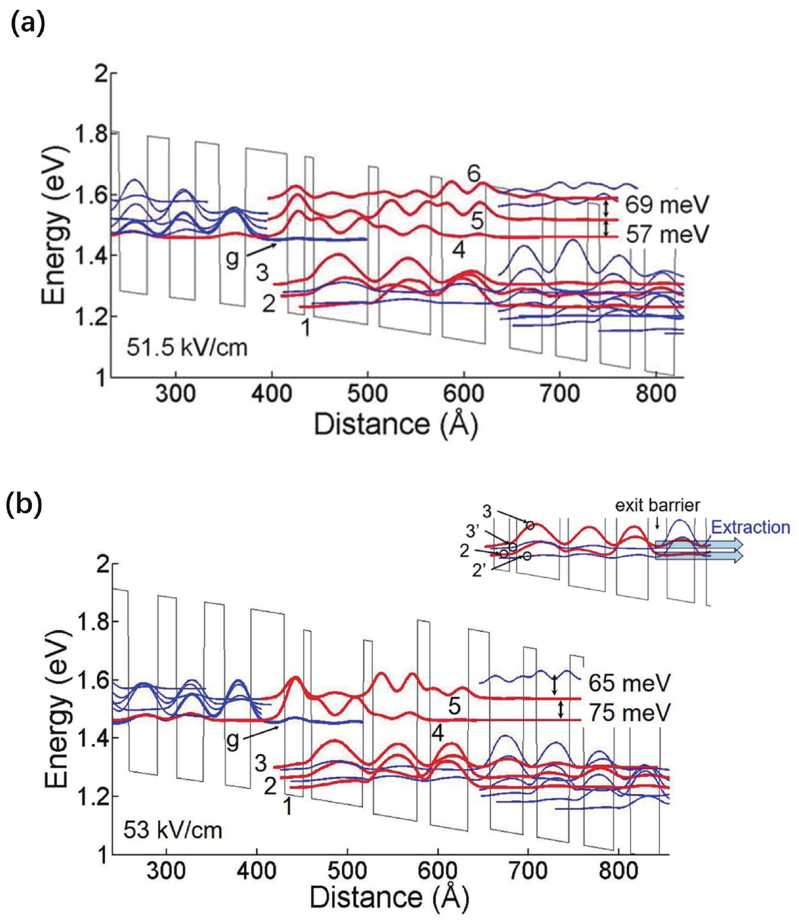
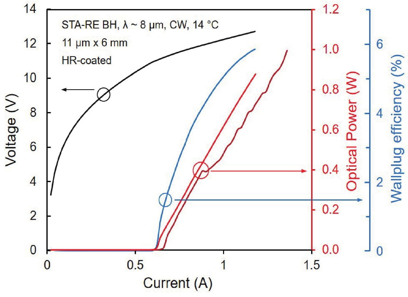
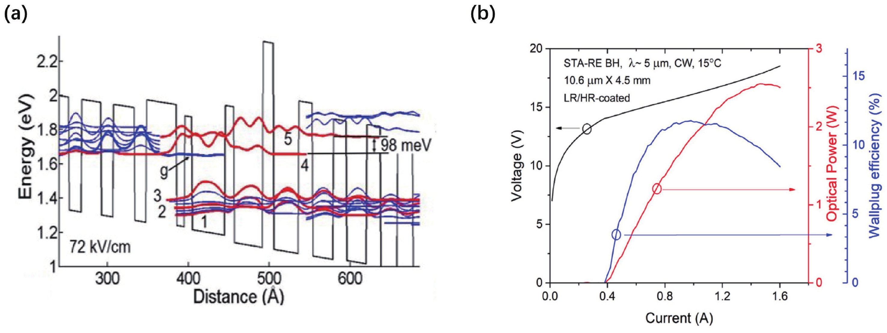
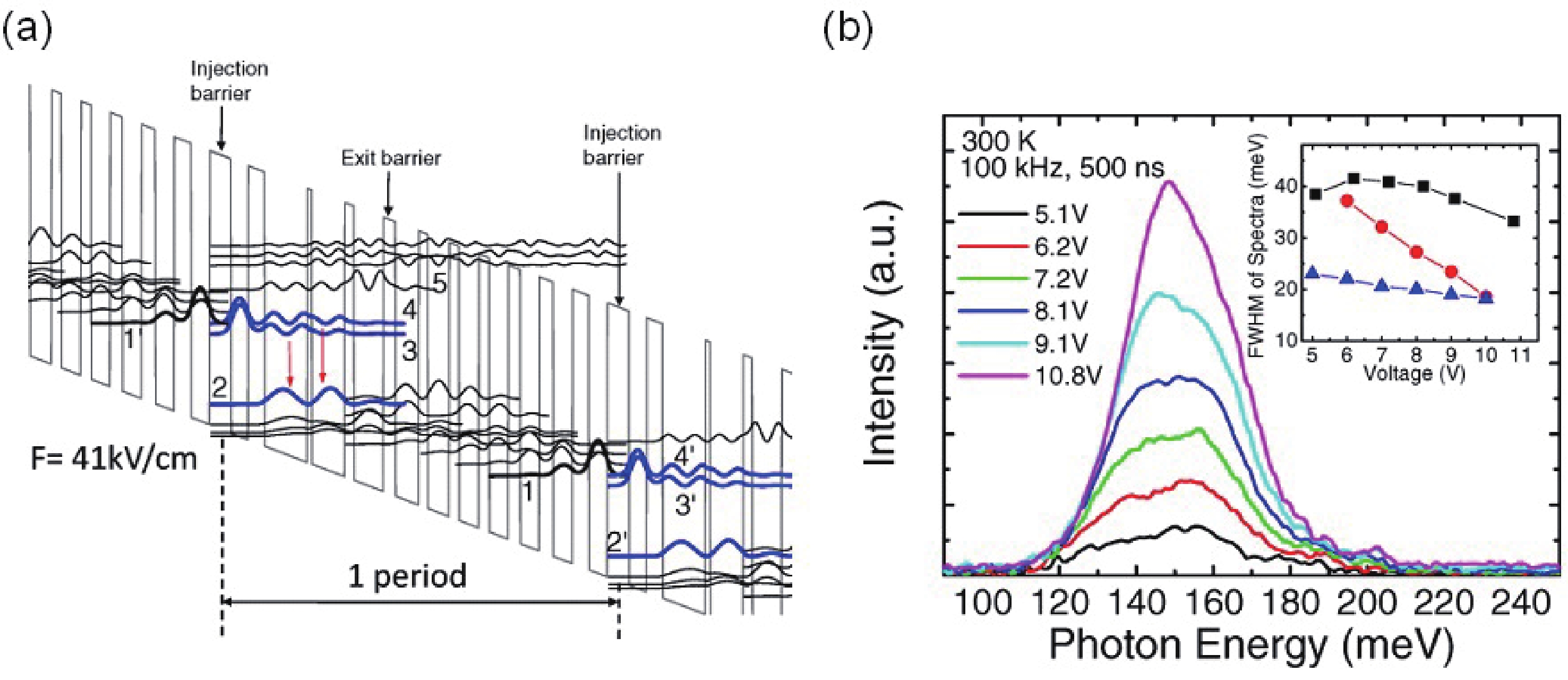
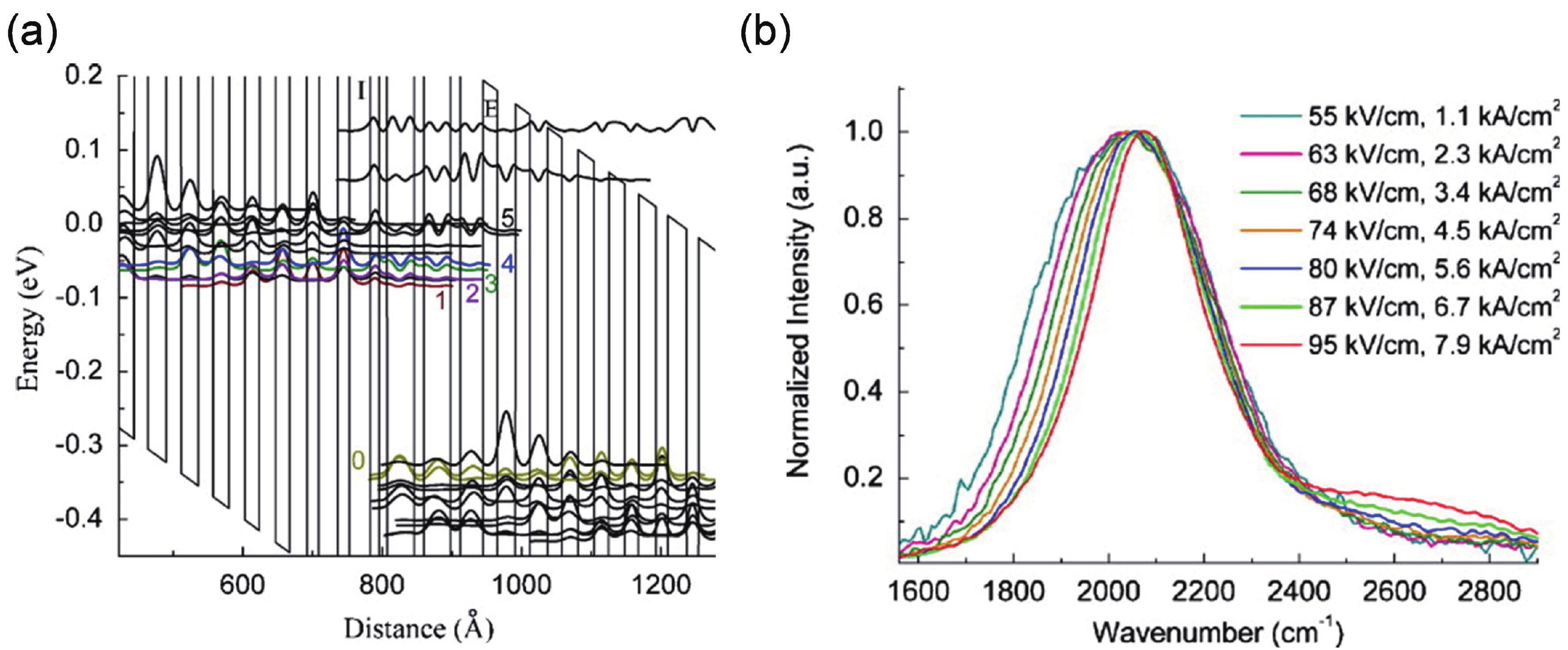
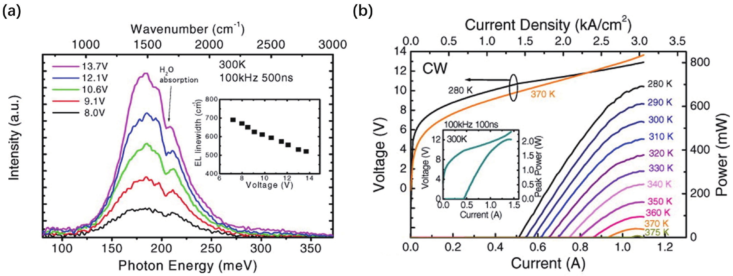
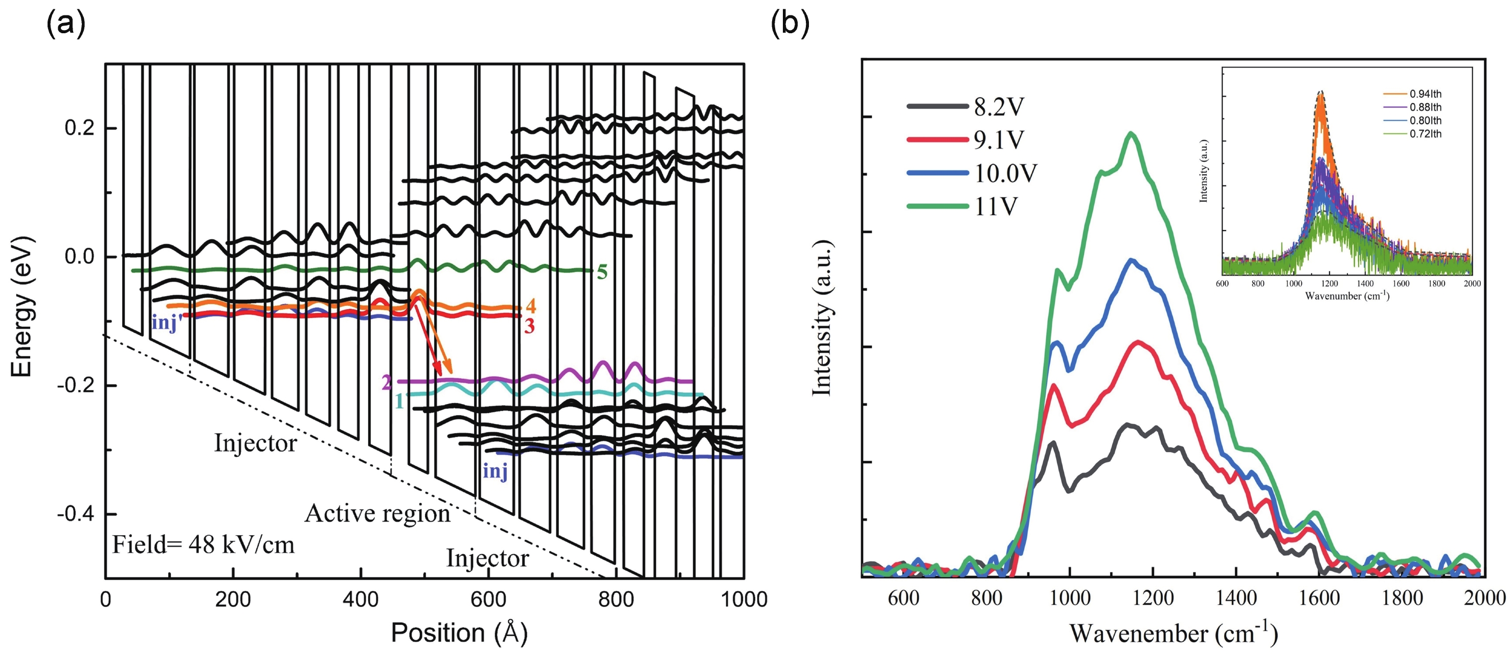
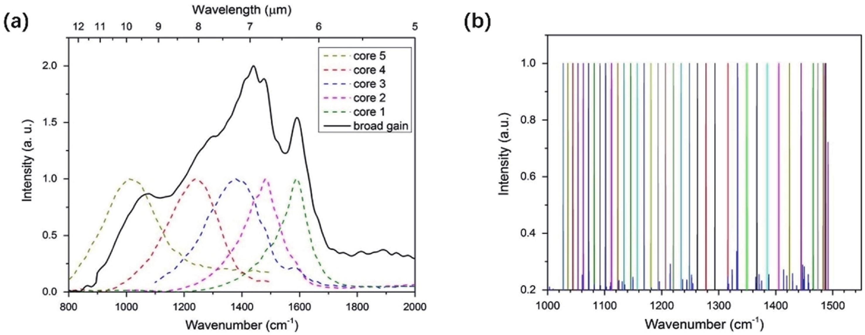
Sharing the advantages of high optical power, high efficiency and design flexibility in a compact size, quantum cascade lasers (QCLs) are excellent mid-to-far infrared laser sources for gas sensing, infrared spectroscopic, medical diagnosis, and defense applications. Metalorganic chemical vapor deposition (MOCVD) is an important technology for growing high quality semiconductor materials, and has achieved great success in the semiconductor industry due to its advantages of high efficiency, short maintenance cycles, and high stability and repeatability. The utilization of MOCVD for the growth of QCL materials holds a significant meaning for promoting the large batch production and industrial application of QCL devices. This review summarizes the recent progress of QCLs grown by MOCVD. Material quality and the structure design together determine the device performance. Research progress on the performance improvement of MOCVD-grown QCLs based on the optimization of material quality and active region structure are mainly reviewed.


J. Semicond.
2023, 44(12): 122001 doi: 10.1088/1674-4926/44/12/122001
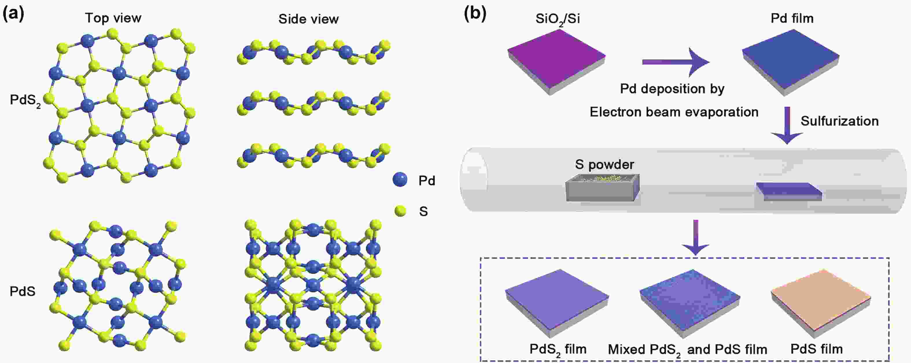
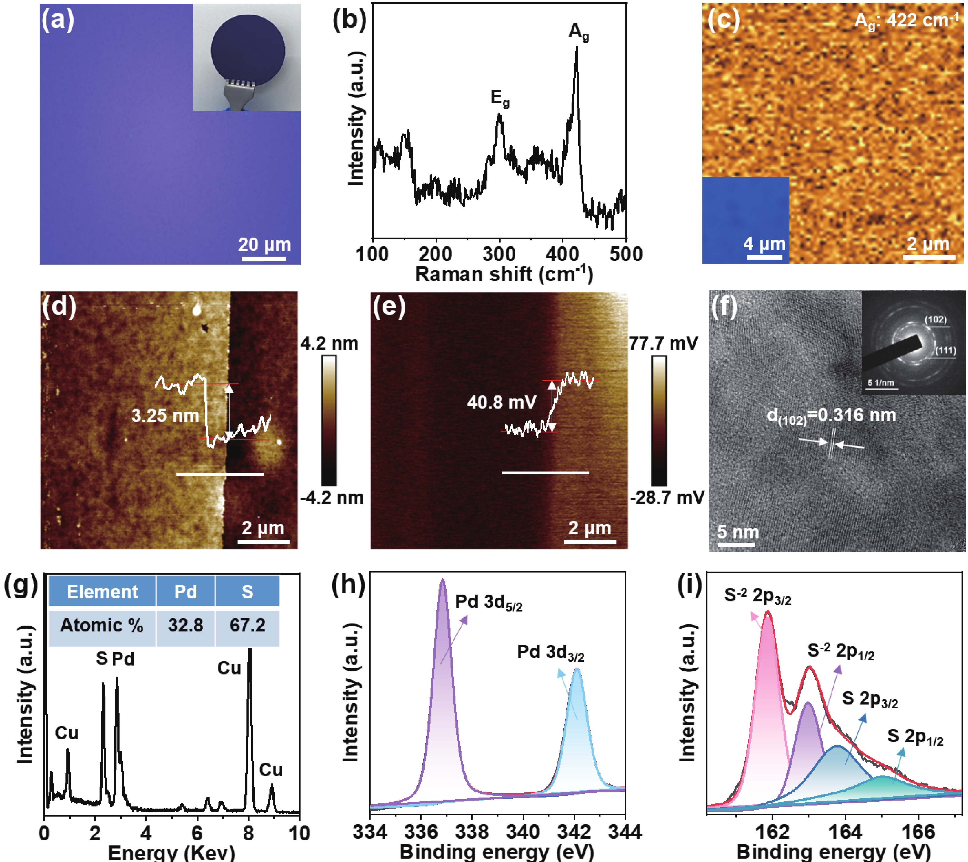
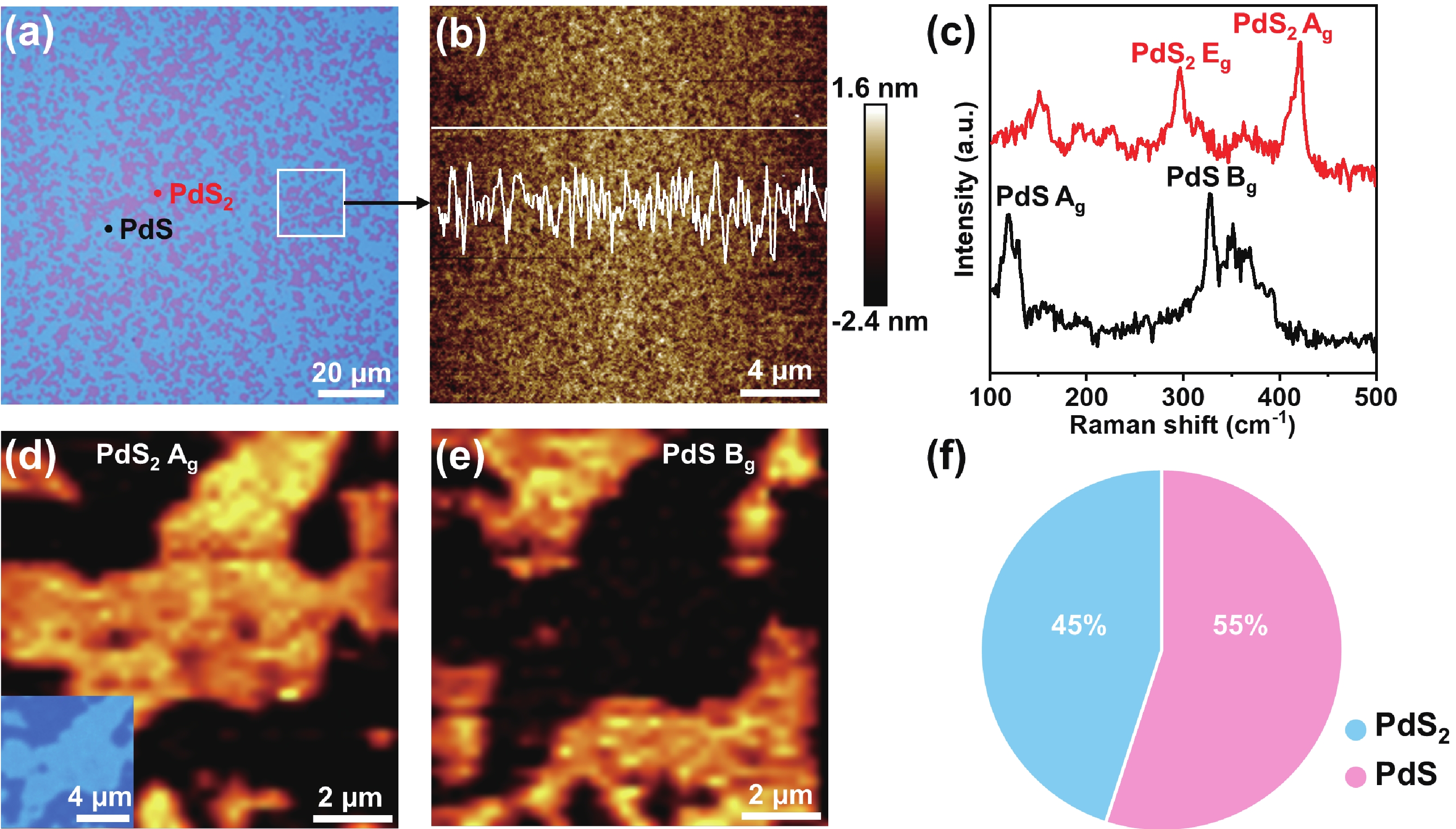
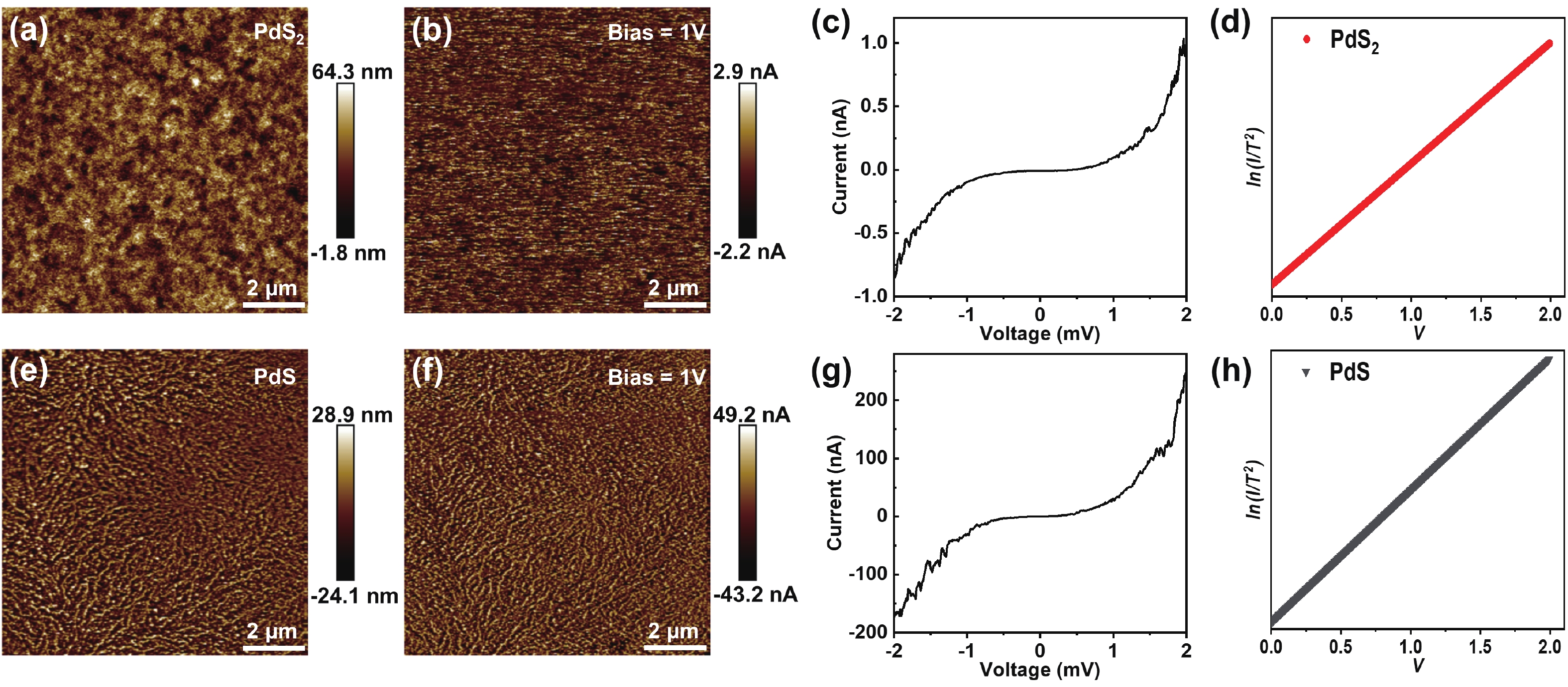
Palladium (Pd)-based sulfides have triggered extensive interest due to their unique properties and potential applications in the fields of electronics and optoelectronics. However, the synthesis of large-scale uniform PdS and PdS2 nanofilms (NFs) remains an enormous challenge. In this work, 2-inch wafer-scale PdS and PdS2 NFs with excellent stability can be controllably prepared via chemical vapor deposition combined with electron beam evaporation technique. The thickness of the pre-deposited Pd film and the sulfurization temperature are critical for the precise synthesis of PdS and PdS2 NFs. A corresponding growth mechanism has been proposed based on our experimental results and Gibbs free energy calculations. The electrical transport properties of PdS and PdS2 NFs were explored by conductive atomic force microscopy. Our findings have achieved the controllable growth of PdS and PdS2 NFs, which may provide a pathway to facilitate PdS and PdS2 based applications for next-generation high performance optoelectronic devices.


J. Semicond.
2023, 44(12): 122101 doi: 10.1088/1674-4926/44/12/122101

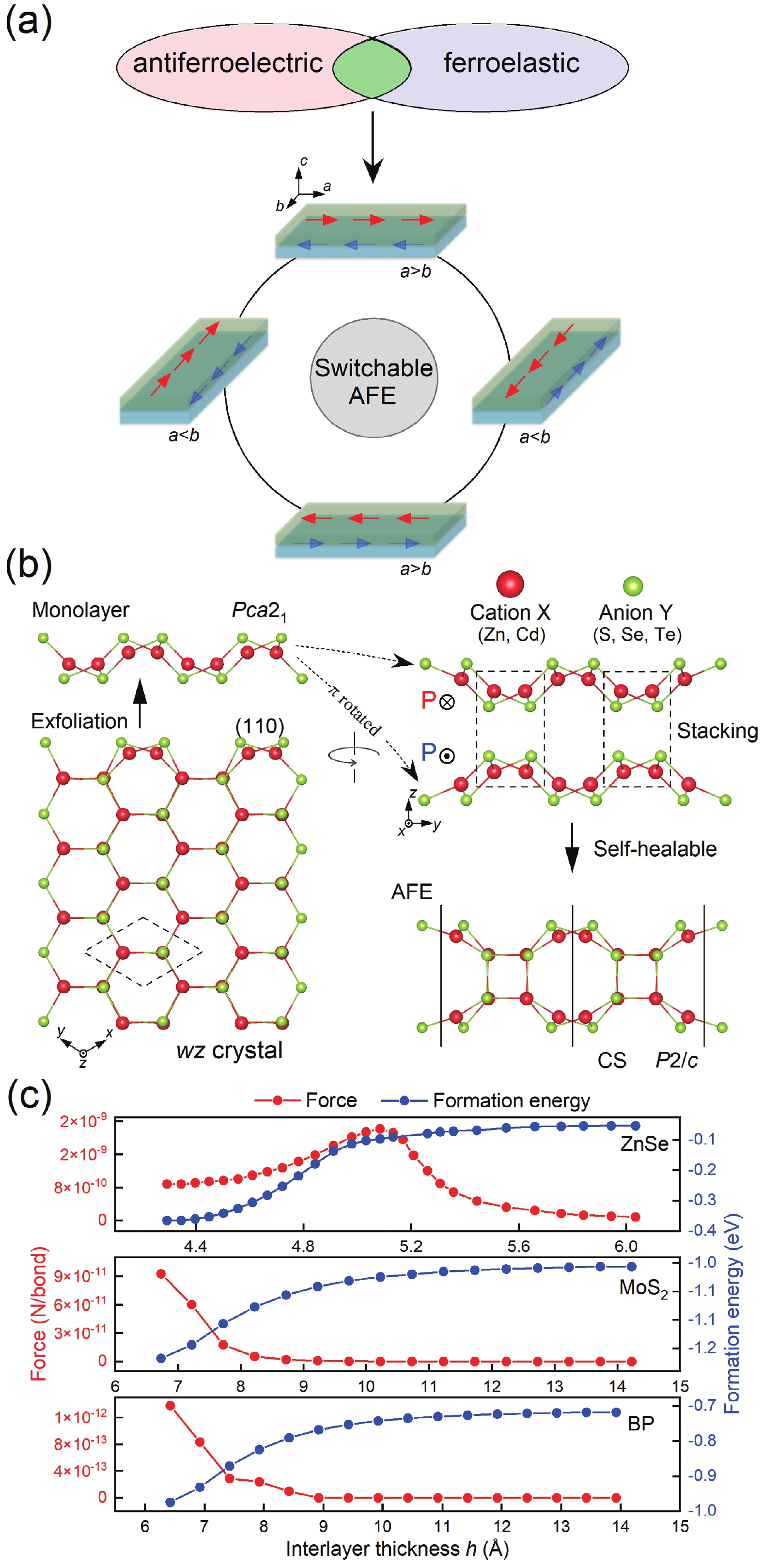
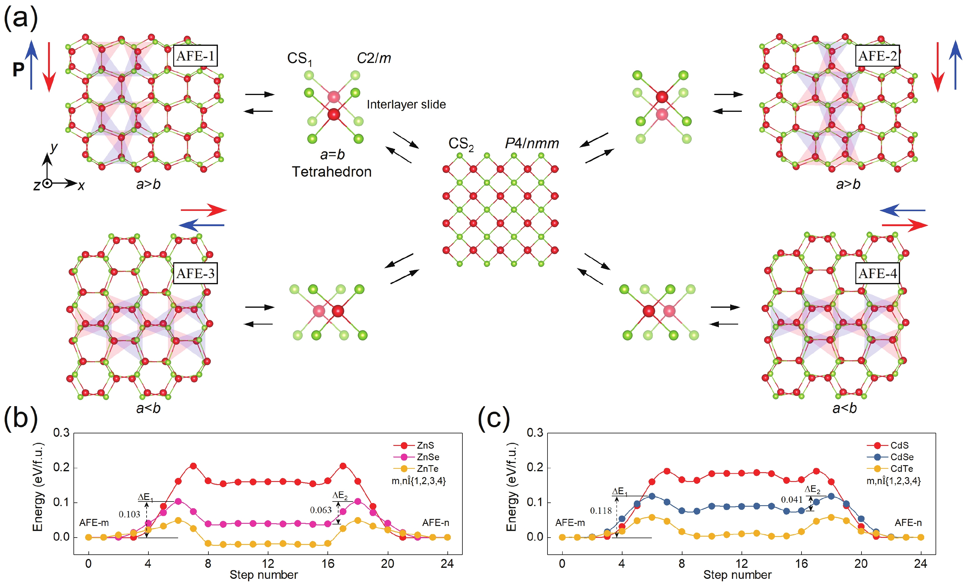
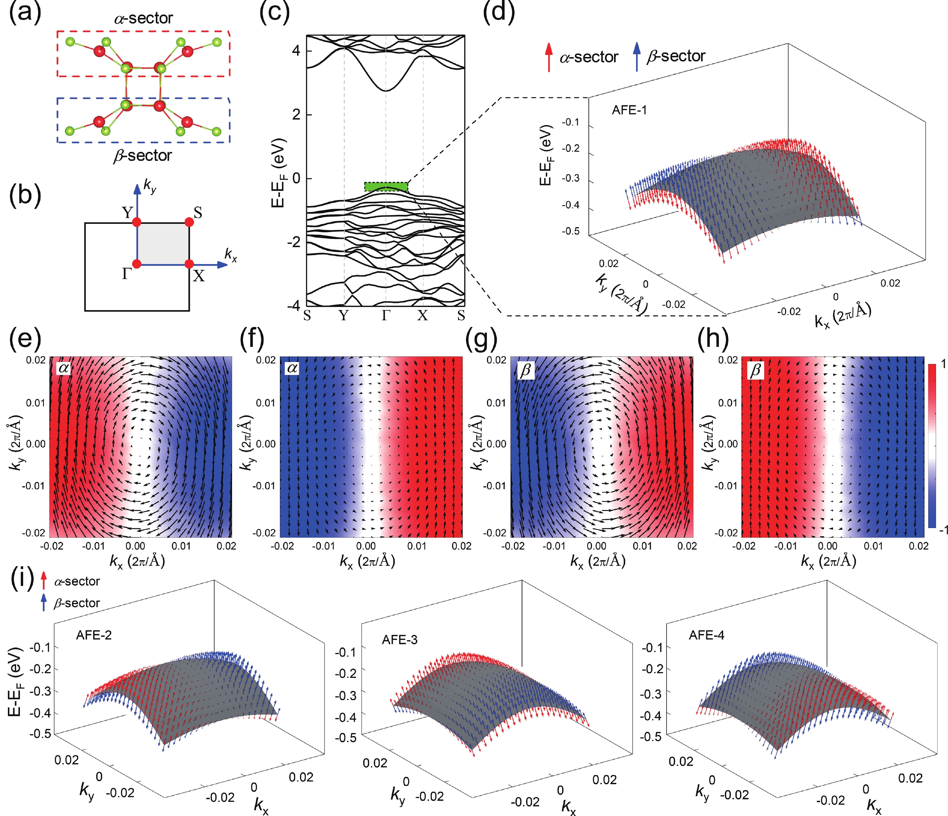
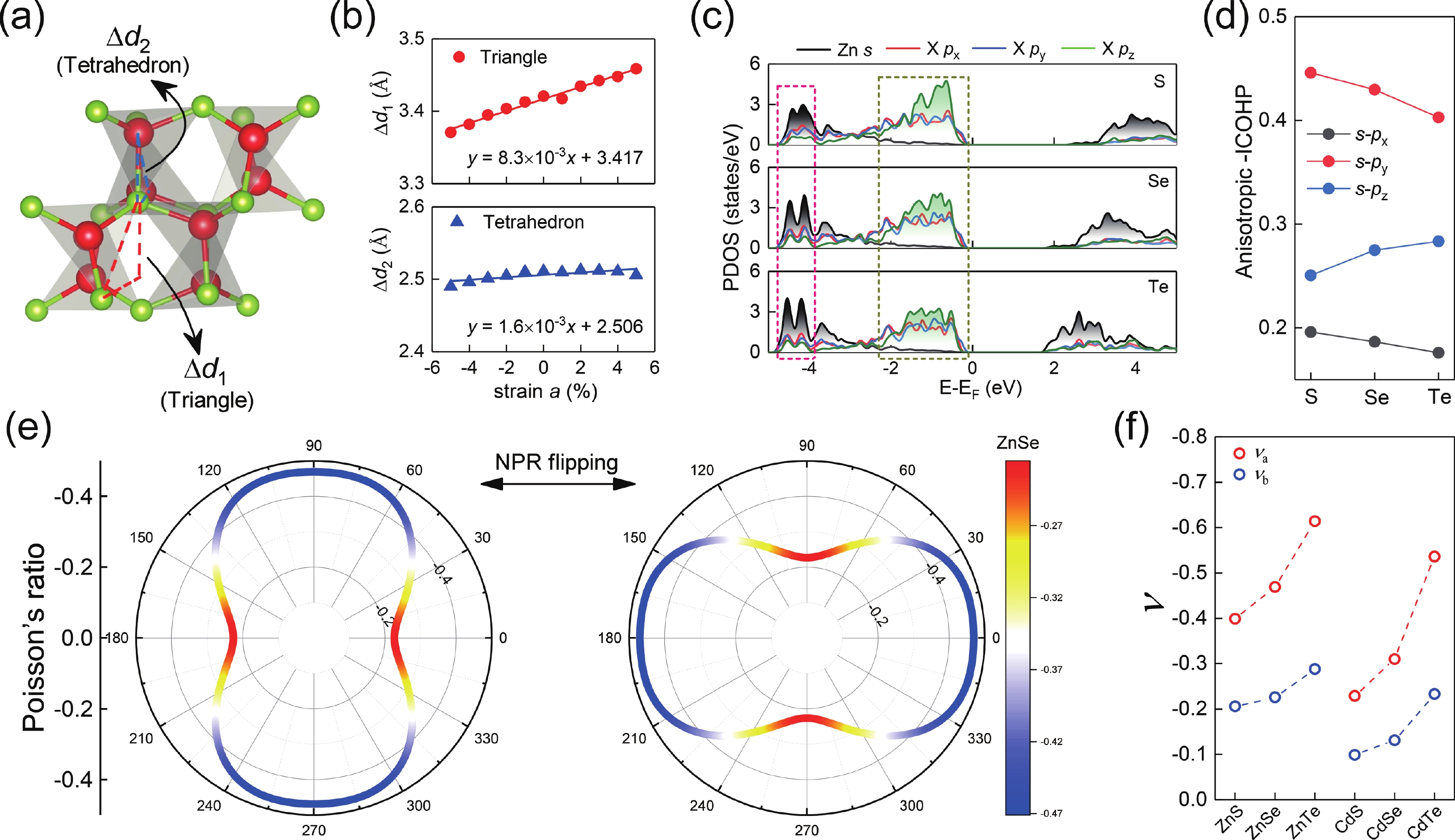
Two-dimensional (2D) antiferroelectric materials have raised great research interest over the last decade. Here, we reveal a type of 2D antiferroelectric (AFE) crystal where the AFE polarization direction can be switched by a certain degree in the 2D plane. Such 2D functional materials are realized by stacking the exfoliated wurtzite (wz) monolayers with “self-healable” nature, which host strongly coupled ferroelasticity/antiferroelectricity and benign stability. The AFE candidates, i.e., ZnX and CdX (X = S, Se, Te), are all semiconductors with direct bandgap at Γ point, which harbors switchable antiferroelectricity and ferroelasticity with low transition barriers, hidden spin polarization, as well as giant in-plane negative Poisson's ratio (NPR), enabling the co-tunability of hidden spin characteristics and auxetic magnitudes via AFE switching. The 2D AFE wz crystals provide a platform to probe the interplay of 2D antiferroelectricity, ferroelasticity, NPR, and spin effects, shedding new light on the rich physics and device design in wz semiconductors.
J. Semicond.
2023, 44(12): 122501 doi: 10.1088/1674-4926/44/12/122501
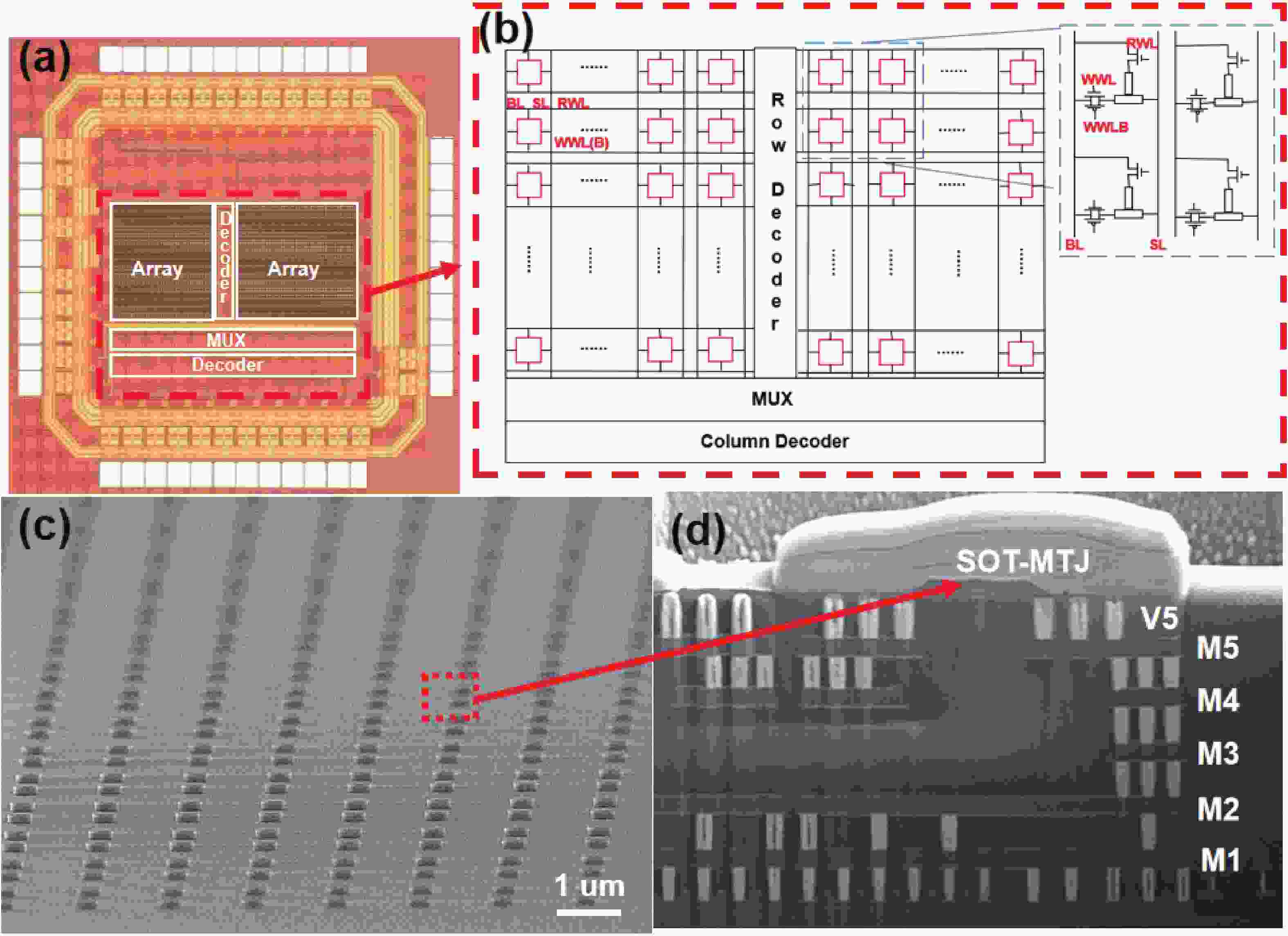
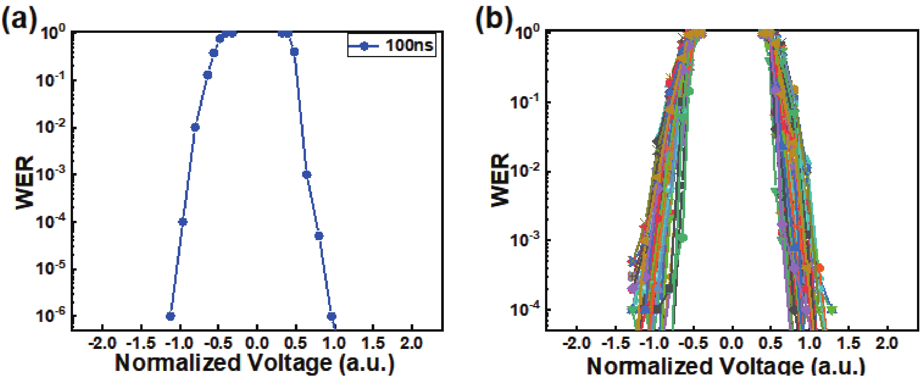
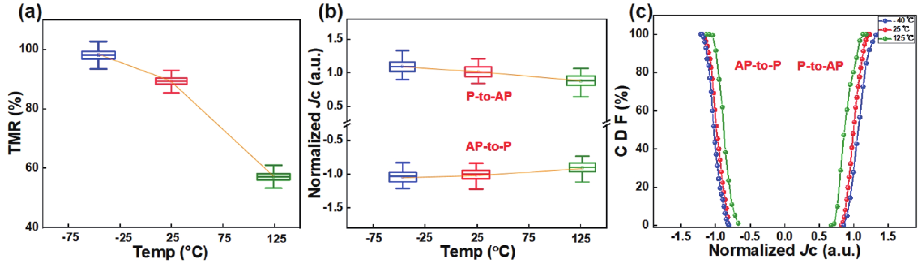
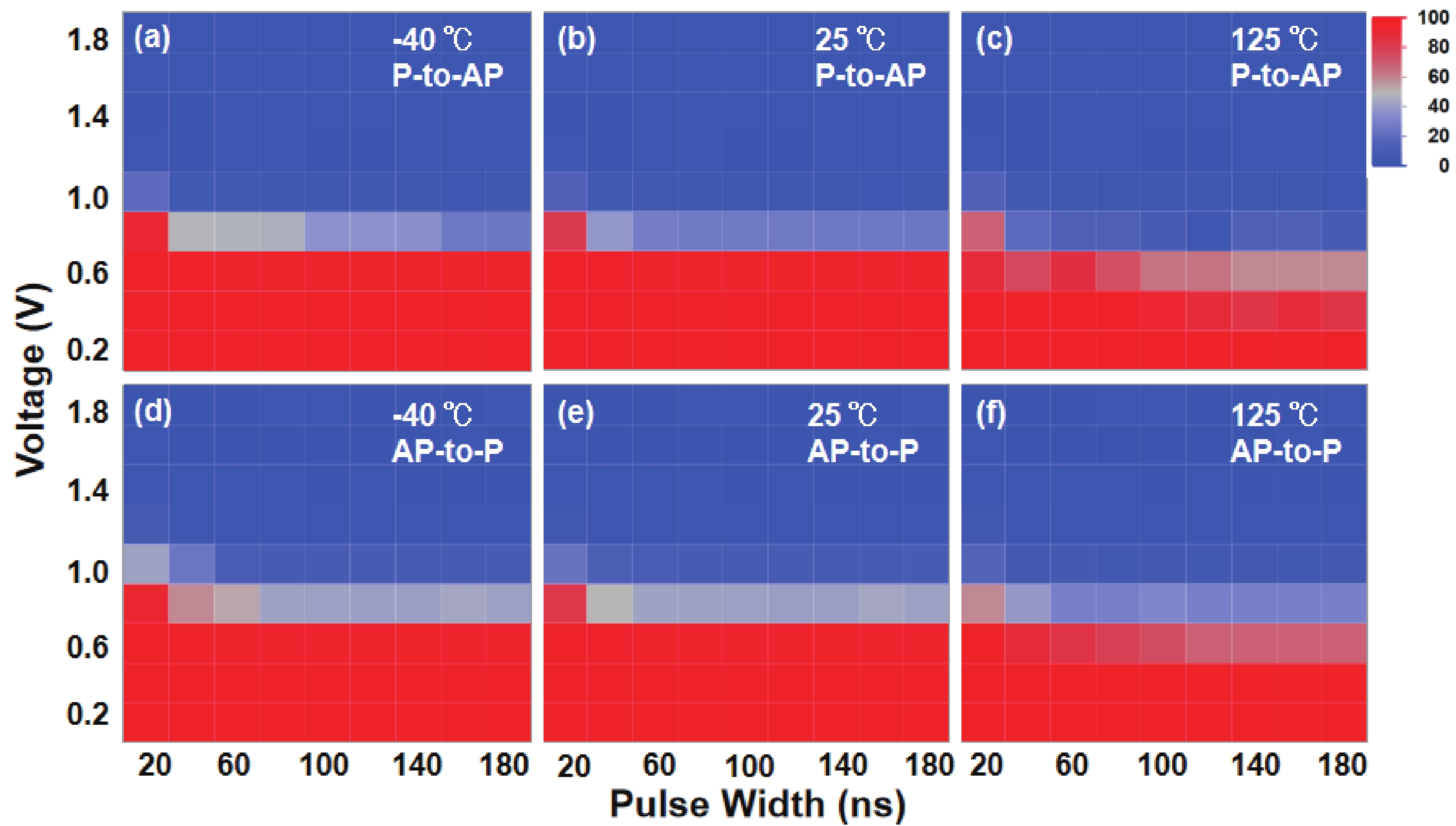
We have successfully demonstrated a 1 Kb spin-orbit torque (SOT) magnetic random-access memory (MRAM) multiplexer (MUX) array with remarkable performance. The 1 Kb MUX array exhibits an in-die function yield of over 99.6%. Additionally, it provides a sufficient readout window, with a TMR/RP_sigma% value of 21.4. Moreover, the SOT magnetic tunnel junctions (MTJs) in the array show write error rates as low as 10−6 without any ballooning effects or back-hopping behaviors, ensuring the write stability and reliability. This array achieves write operations in 20 ns and 1.2 V for an industrial-level temperature range from −40 to 125 °C. Overall, the demonstrated array shows competitive specifications compared to the state-of-the-art works. Our work paves the way for the industrial-scale production of SOT-MRAM, moving this technology beyond R&D and towards widespread adoption.


J. Semicond.
2023, 44(12): 122502 doi: 10.1088/1674-4926/44/12/122502
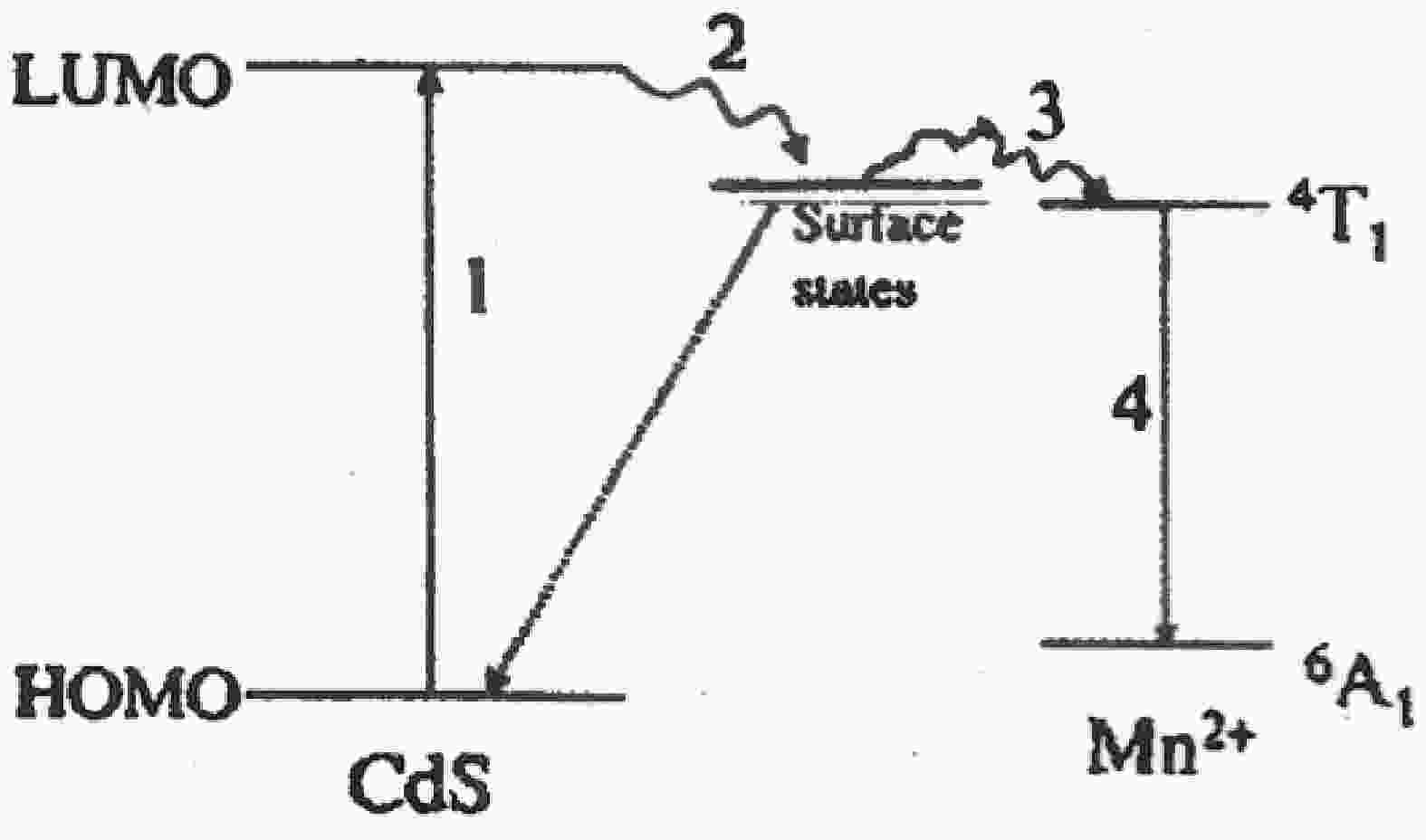
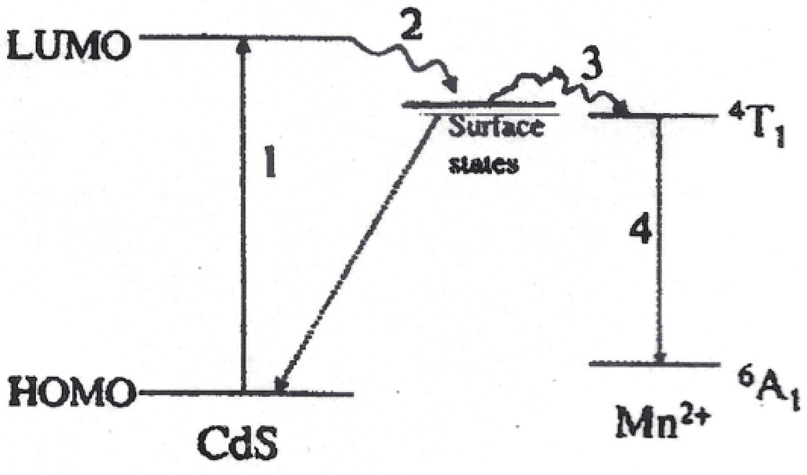
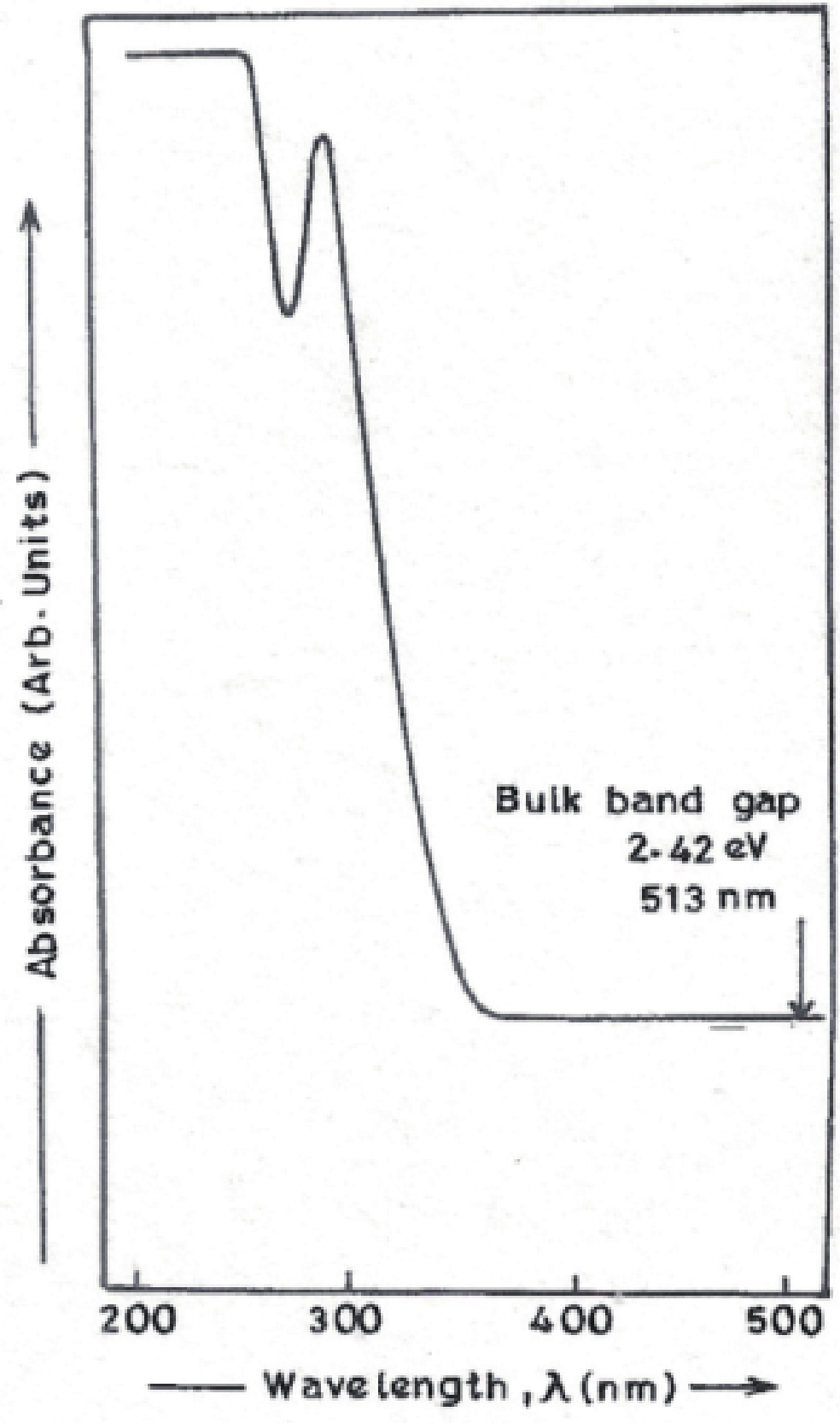
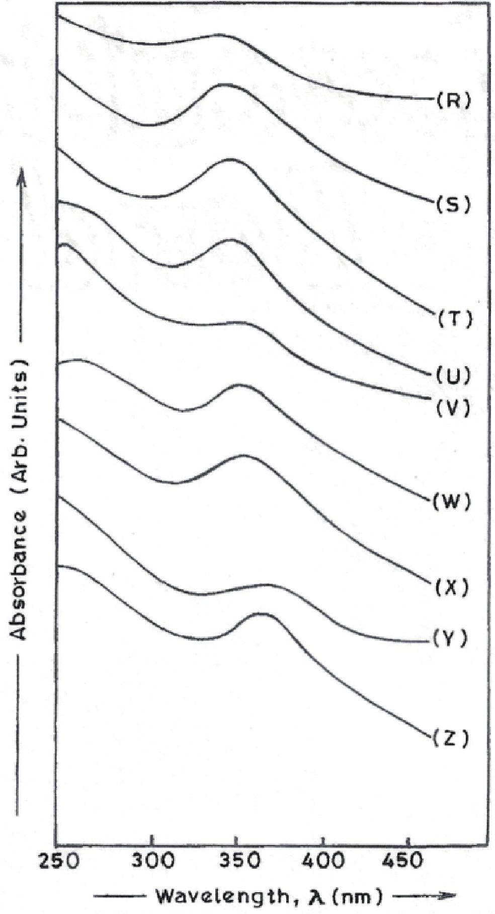
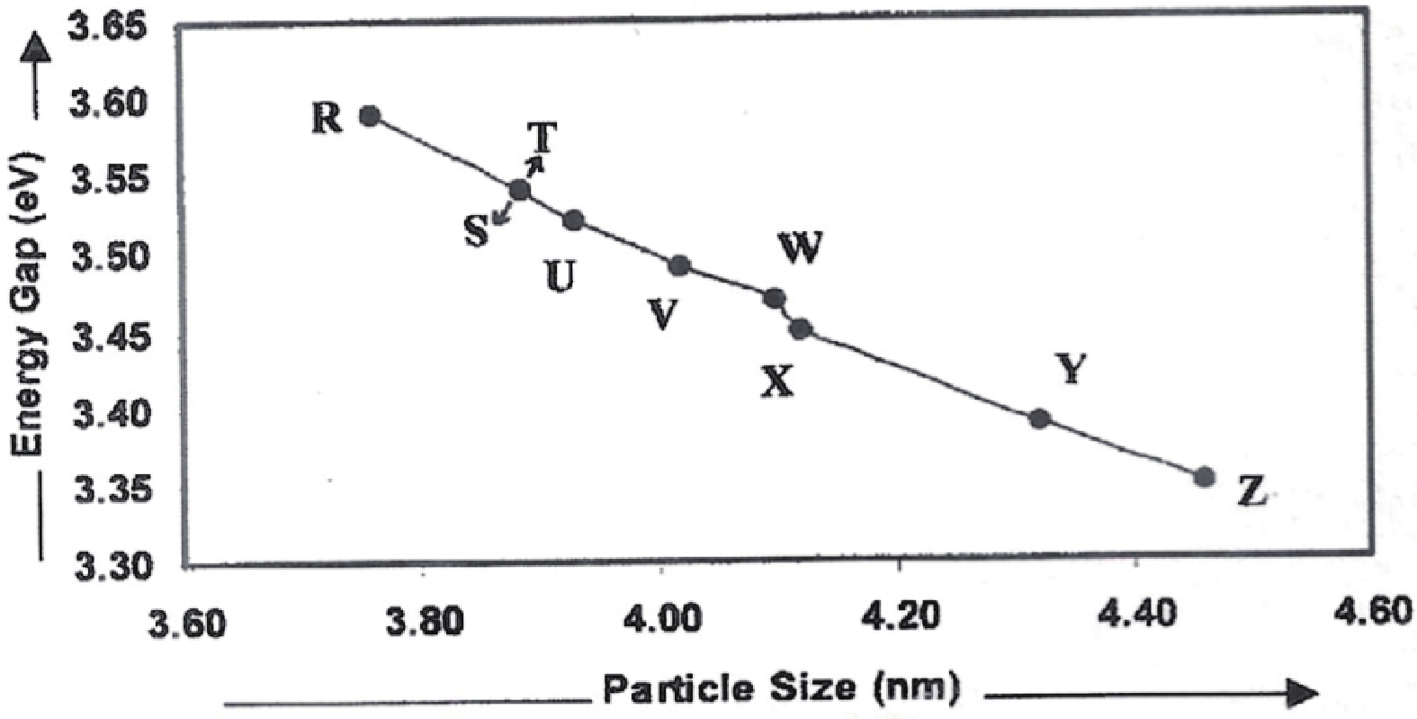
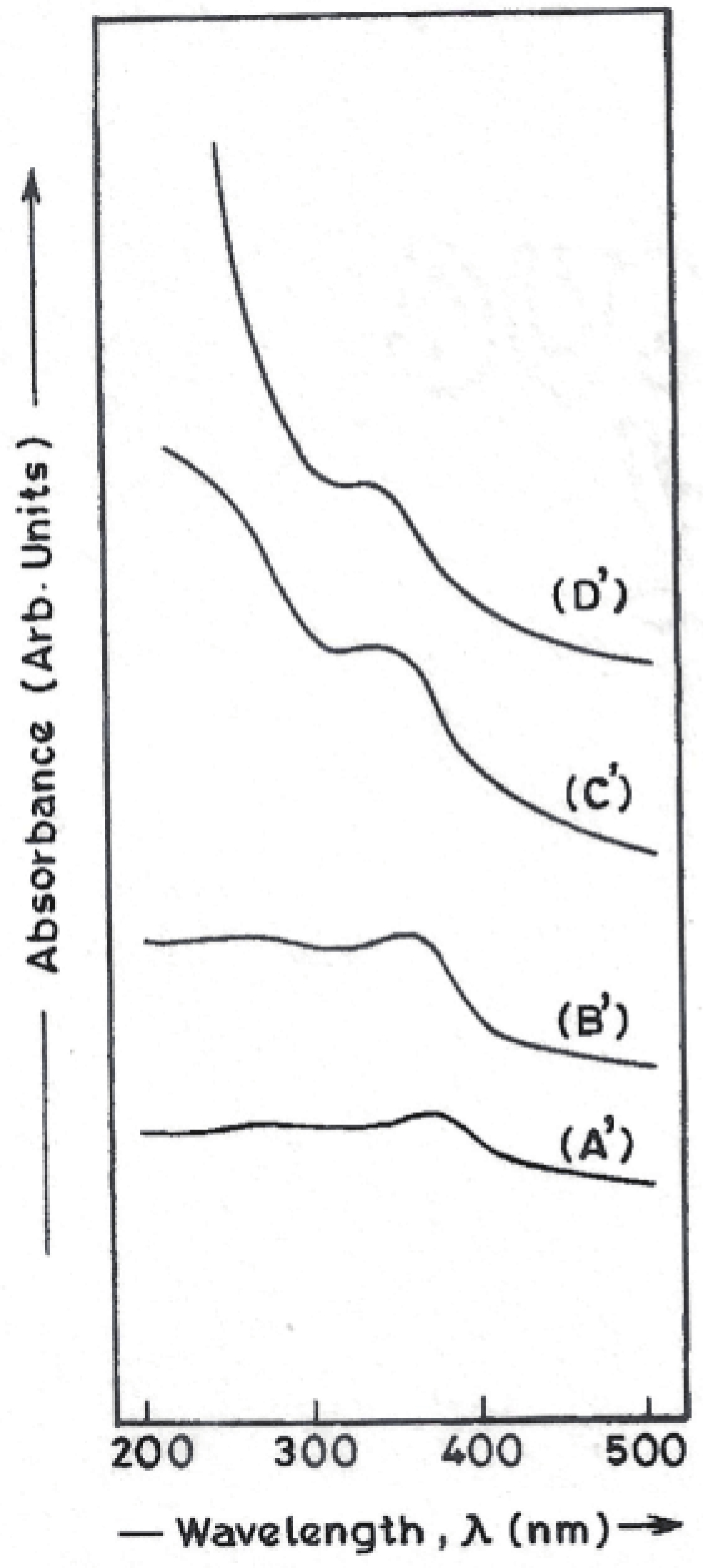
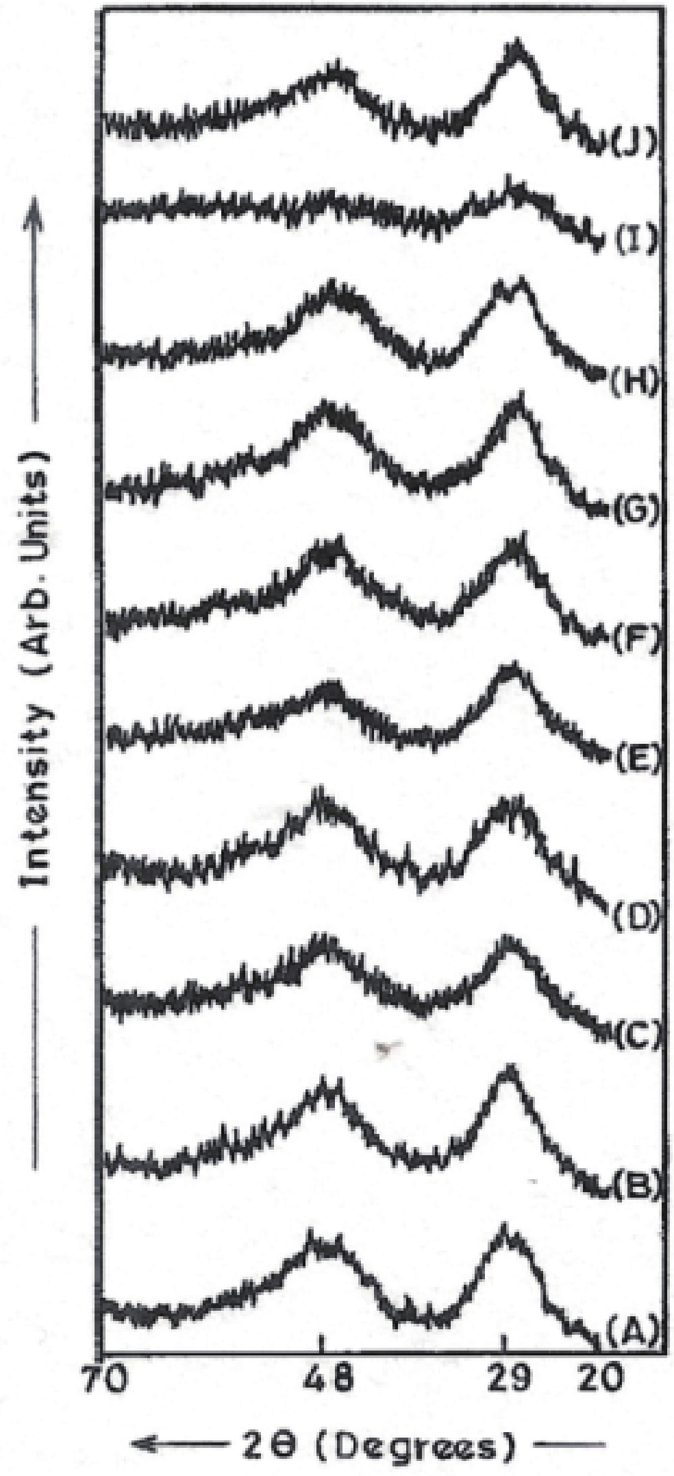
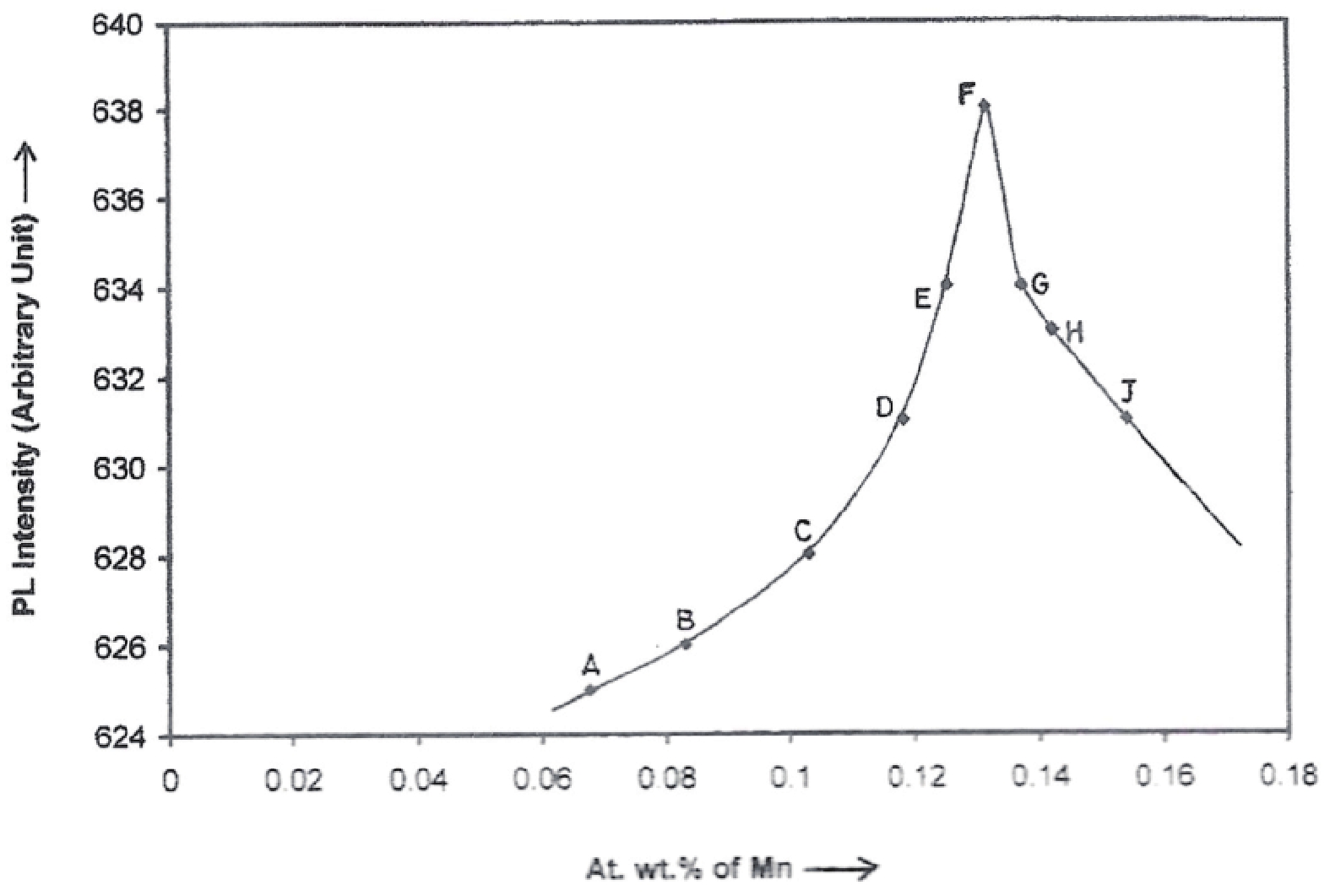
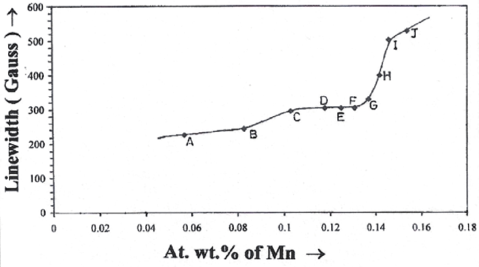
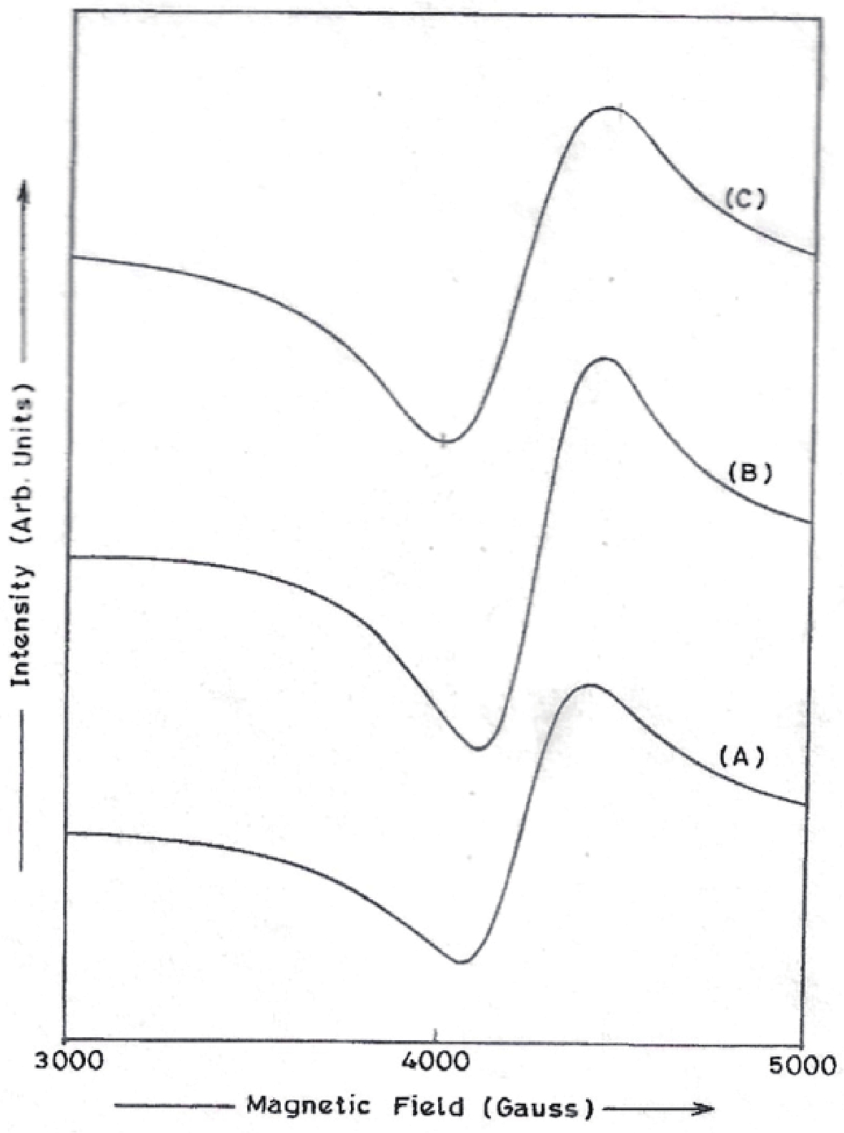
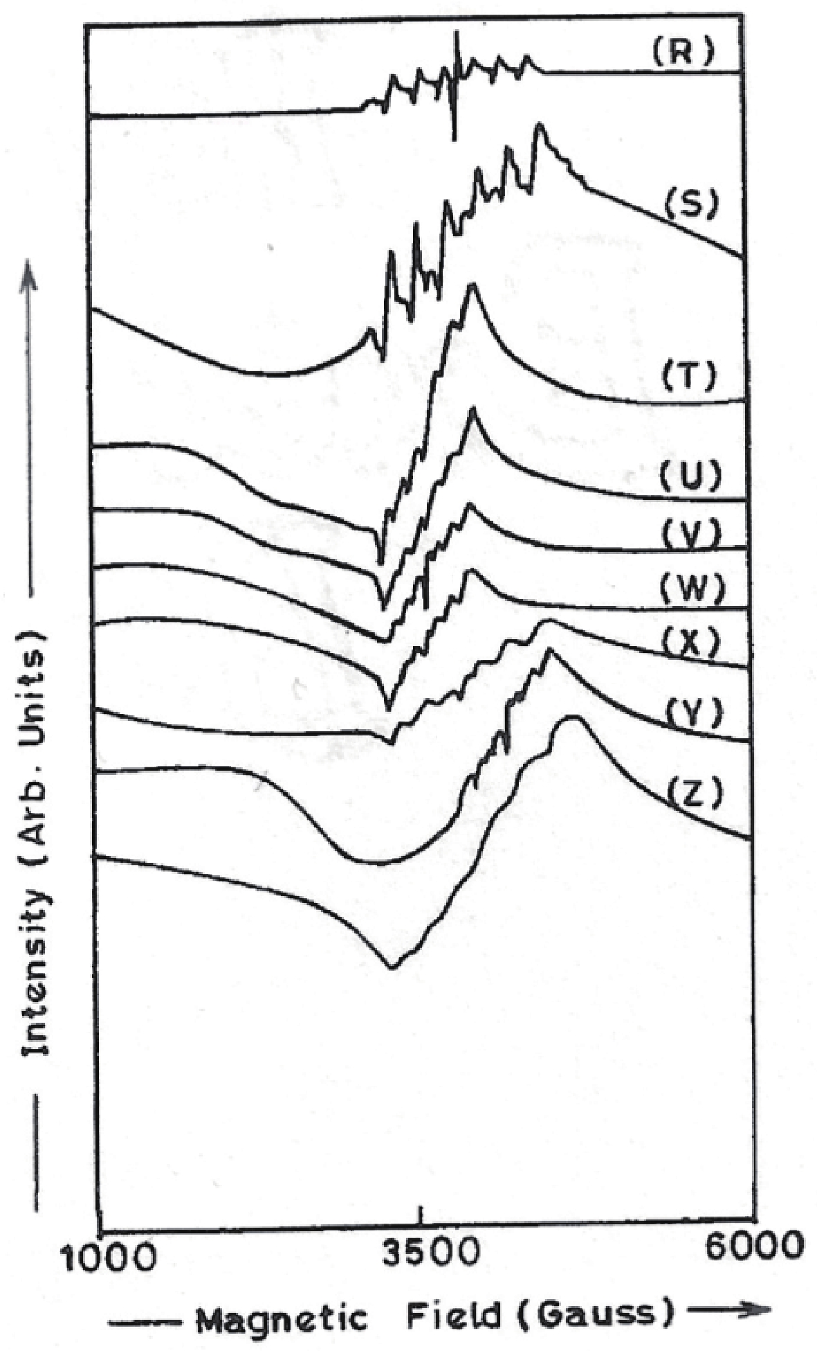
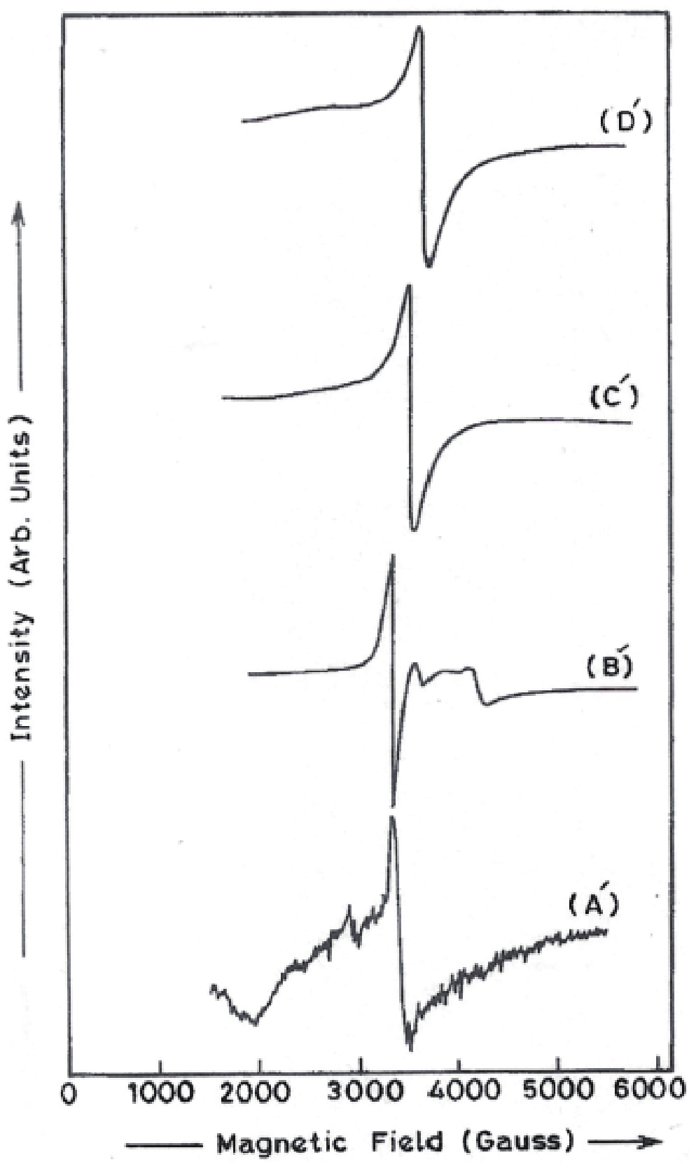
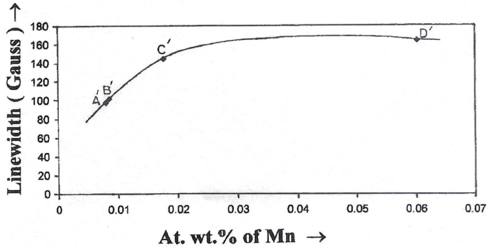
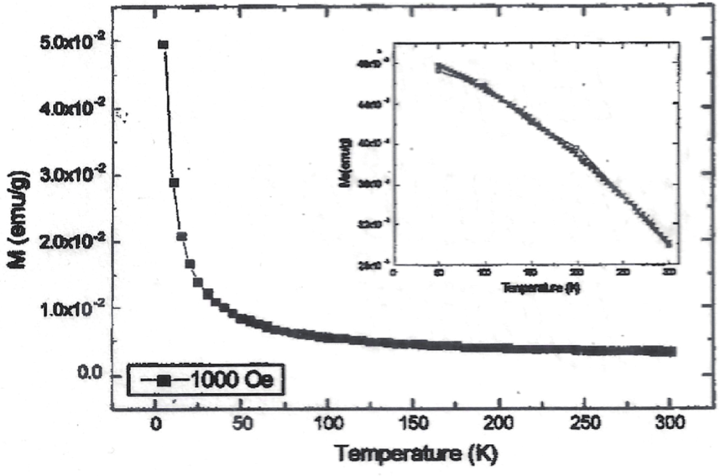
Manganese (Mn) doped cadmium sulphide (CdS) nanoparticles were synthesized using a chemical method. It was possible to decrease CdS : Mn particle size by increasing Mn concentration. Investigation techniques such as ultraviolet−visible (UV−Vis) absorption spectroscopy and photoluminescence (PL) spectroscopy were used to determine optical properties of CdS : Mn nanoparticles. Size quantization effect was observed in UV−Vis absorption spectra. Quantum efficiency for luminescence or the internal magnetic field strength was increased by doping CdS nanoparticles with Mn element. Orange emission was observed at wavelength ~630 nm due to 4T1 → 6A1 transition. Isolated Mn2+ ions arranged in tetrahedral coordination are mainly responsible for luminescence. Luminescence quenching and the effect of Mn doping on hyperfine interactions in the case of CdS nanoparticles were also discussed. The corresponding weight percentage of Mn element actually incorporated in doping process was determined by atomic absorption spectroscopy (AAS). Crystallinity was checked and the average size of nanoparticles was estimated using the X-ray diffraction (XRD) technique. CdS : Mn nanoparticles show ferromagnetism at room temperature. Transmission electron microscopy (TEM) images show spherical clusters of various sizes and selected area electron diffraction (SAED) patterns show the polycrystalline nature of the clusters. The electronic states of diluted magnetic semiconductors (DMS) of Ⅱ−Ⅵ group CdS nanoparticles give them great potential for applications due to quantum confinement. In this study, experimental results and discussions on these aspects have been given.


J. Semicond.
2023, 44(12): 122701 doi: 10.1088/1674-4926/44/12/122701

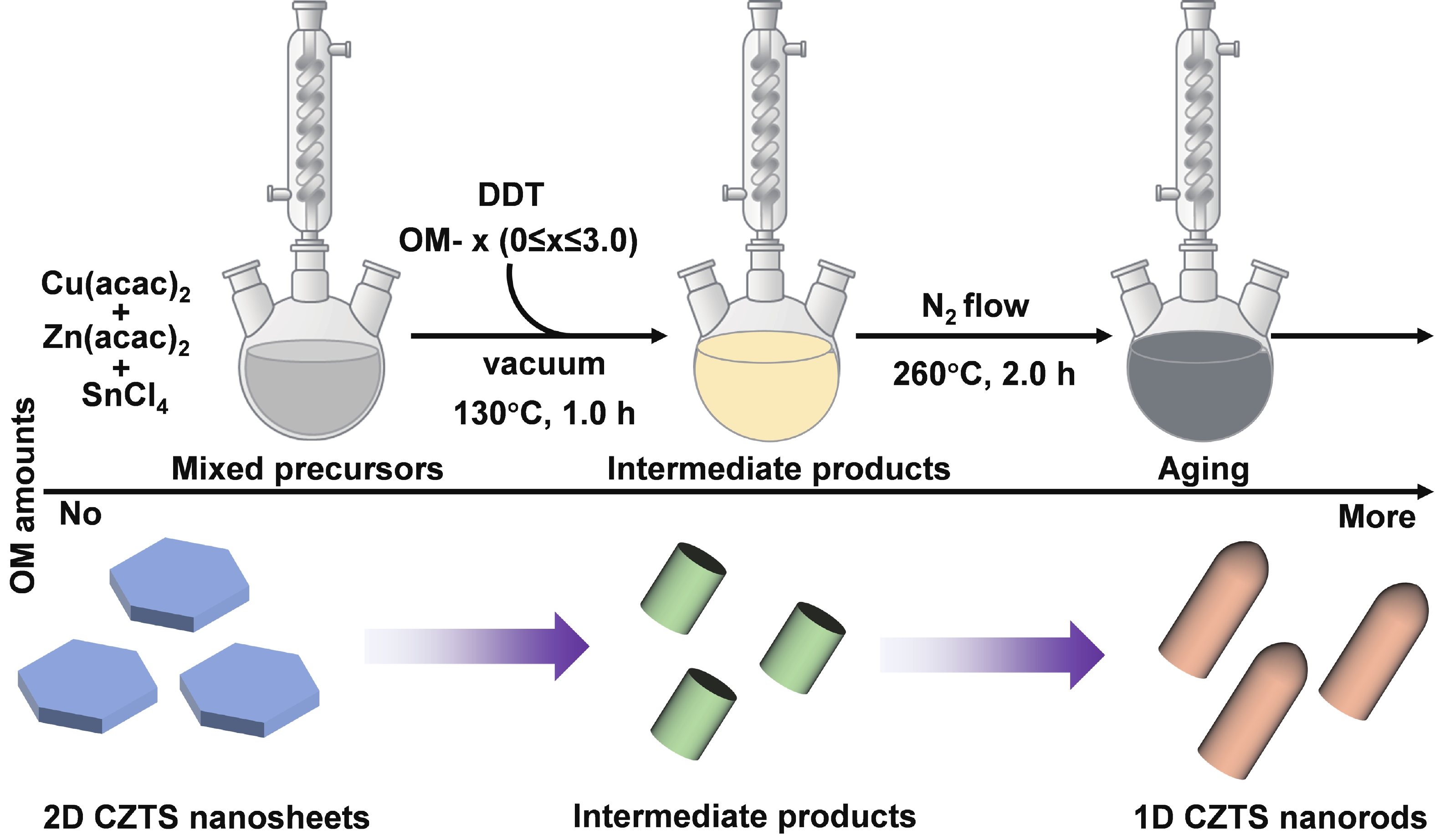
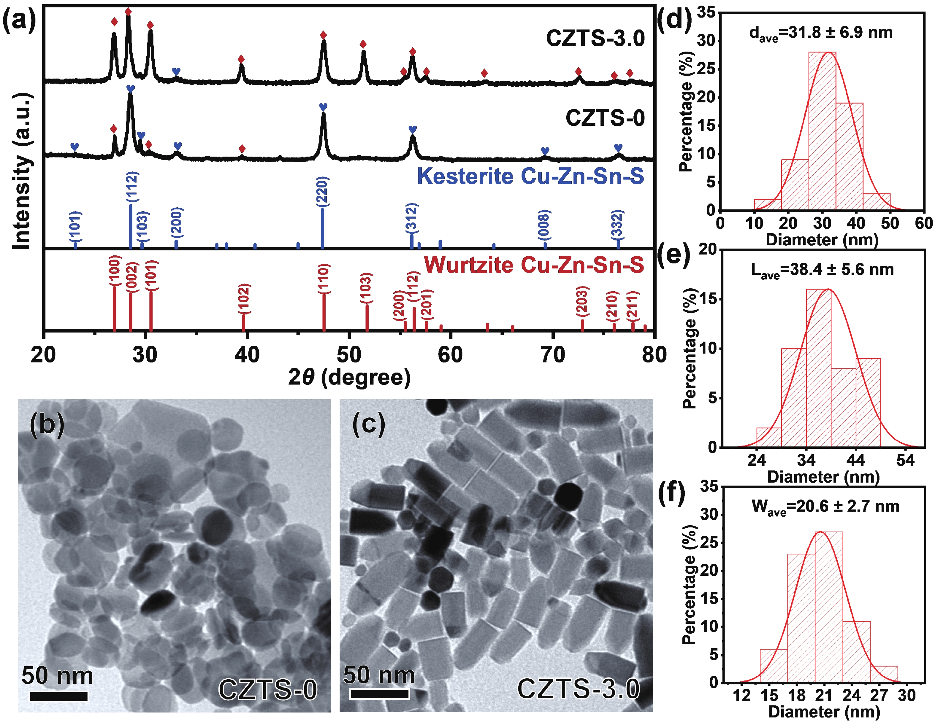
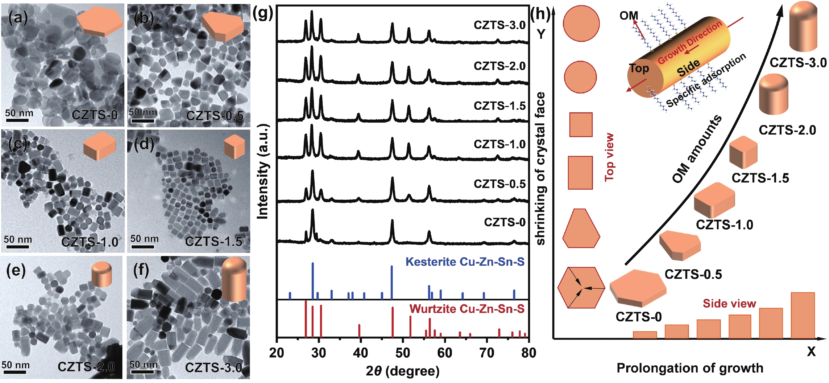
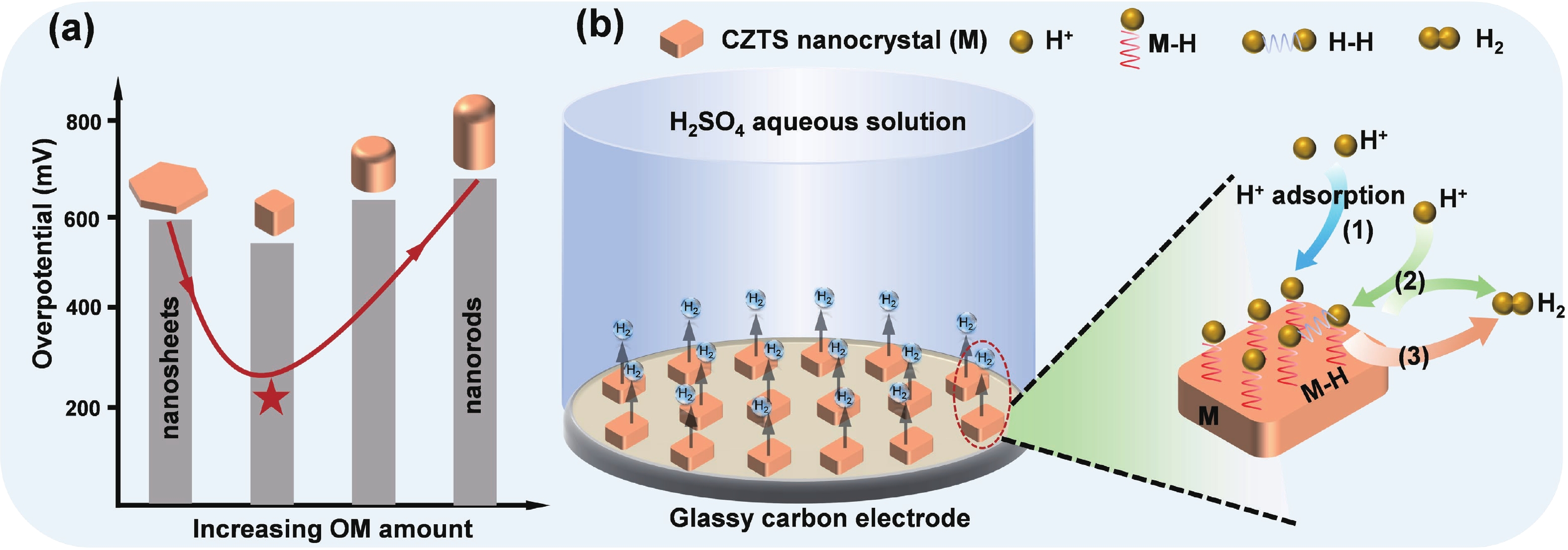
As typical quarternary copper-based chalcogenides, Cu–Zn–Sn–S nanocrystals (CZTS NCs) have emerged as a new-fashioned electrocatalyst in hydrogen evolution reactions (HERs). Oleylamine (OM), a reducing surfactant and solvent, plays a significant role in the assisting synthesis of CZTS NCs due to the ligand effect. Herein, we adopted a facile one-pot colloidal method for achieving the structure evolution of CZTS NCs from 2D nanosheets to 1D nanorods assisted through the continuous addition of OM. During the process, the mechanism of OM-induced morphology evolution was further discussed. When merely adding pure 1-dodecanethiol (DDT) as the solvent, the CZTS nanosheets were obtained. As OM was gradually added to the reaction, the CZTS NCs began to grow along the sides of the nanosheets and gradually shrink at the top, followed by the formation of stable nanorods. In acidic electrolytic conditions, the CZTS NCs with 1.0 OM addition display the optimal HER activity with a low overpotential of 561 mV at 10 mA/cm2 and a small Tafel slope of 157.6 mV/dec compared with other CZTS samples. The enhancement of HER activity could be attributed to the contribution of the synergistic effect of the diverse crystal facets to the reaction.

J. Semicond.
2023, 44(12): 122702 doi: 10.1088/1674-4926/44/12/122702

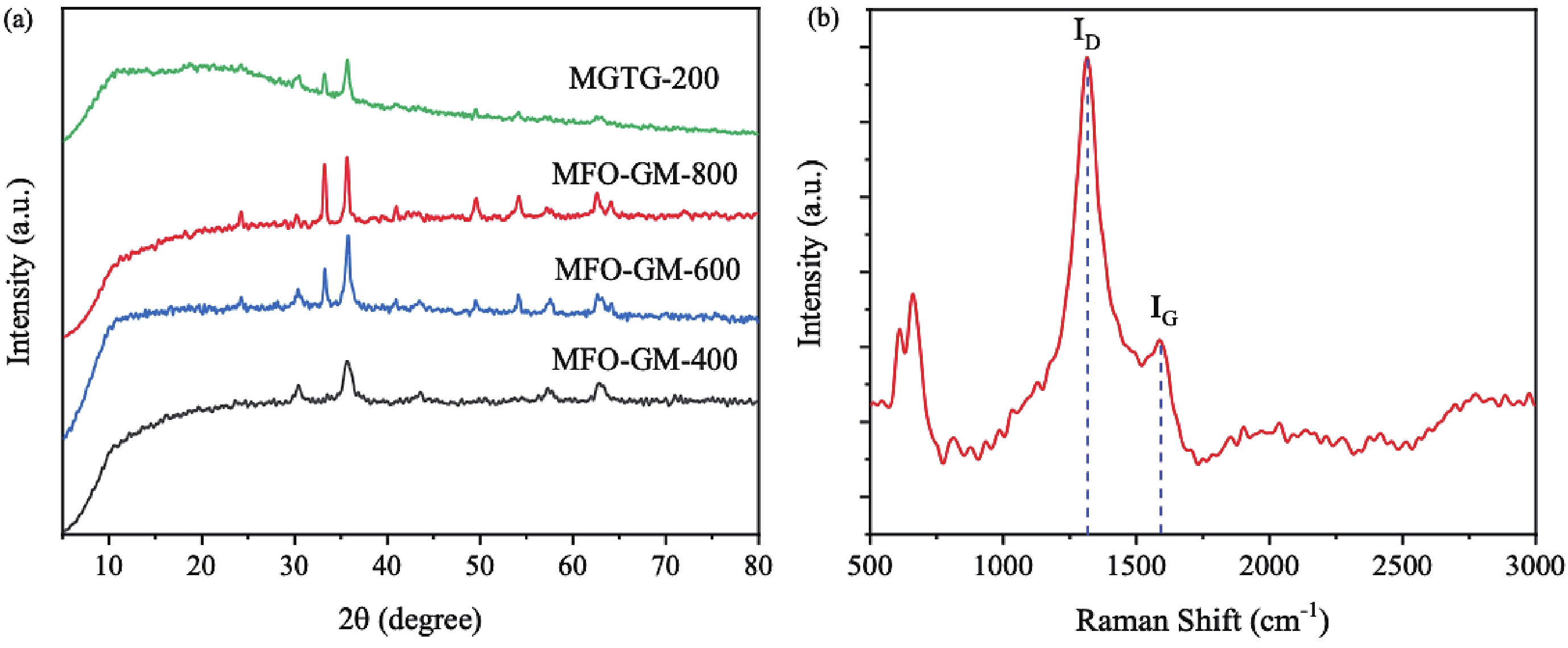
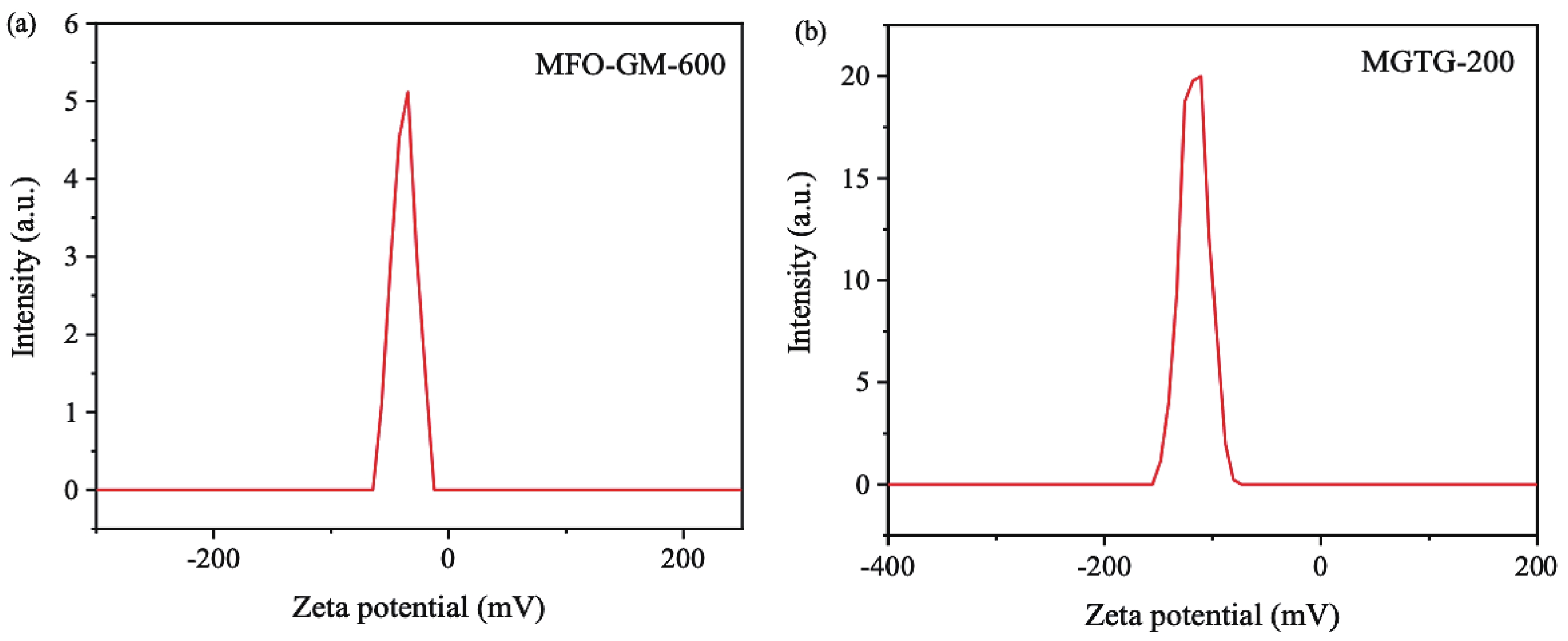
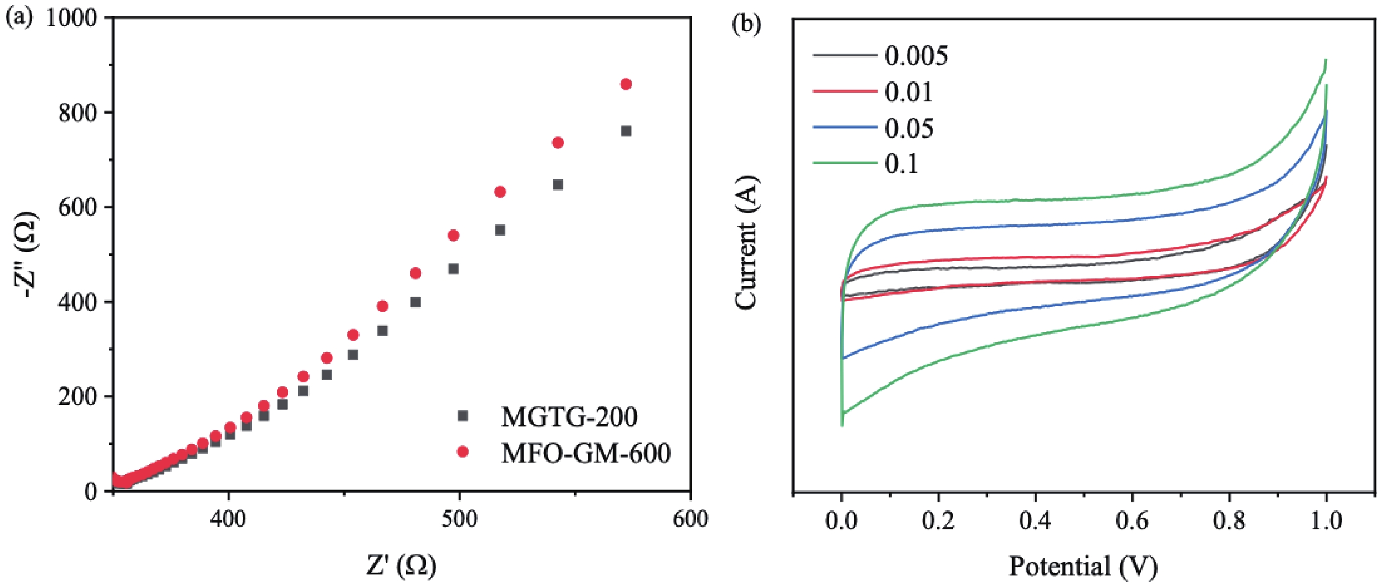
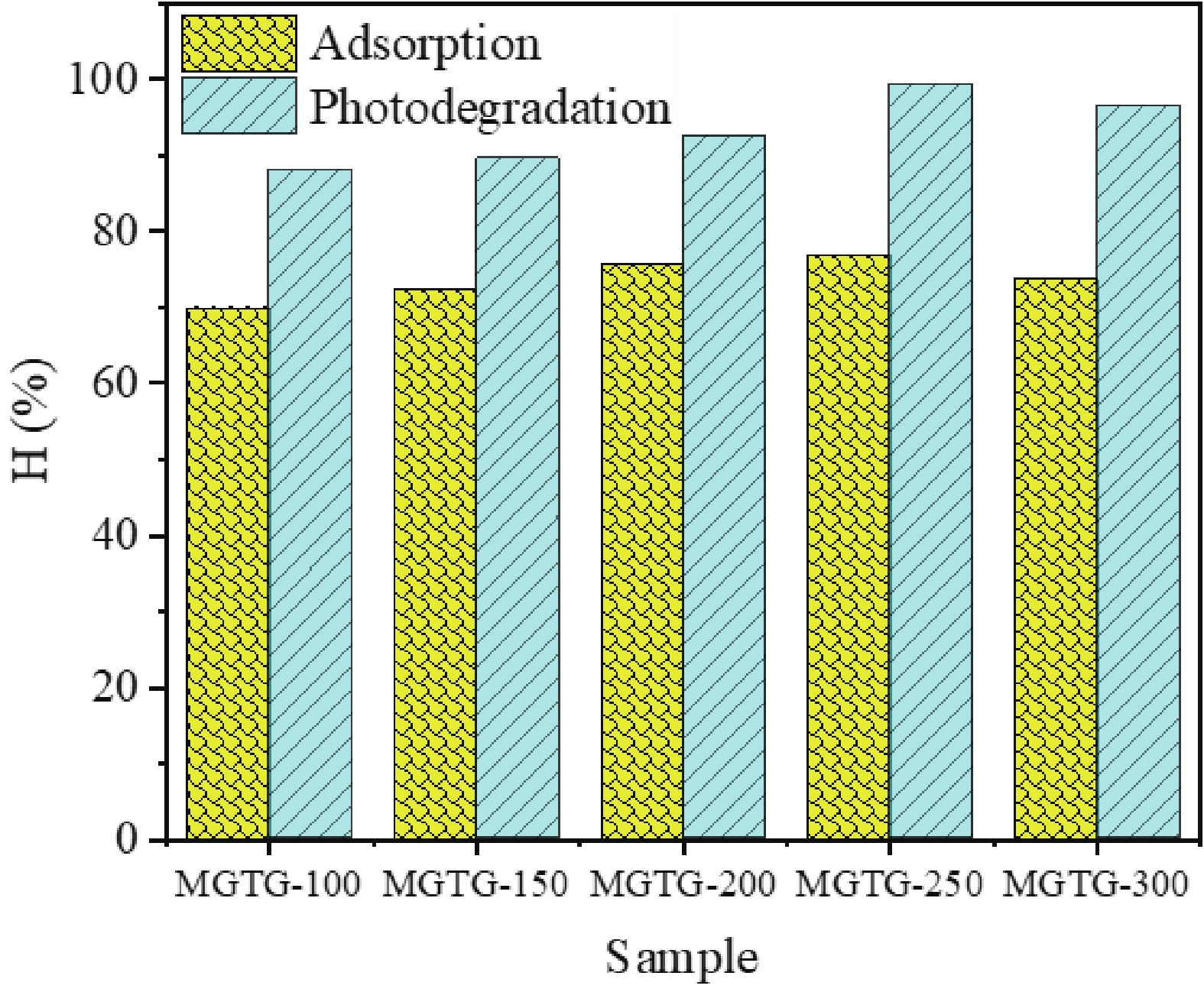
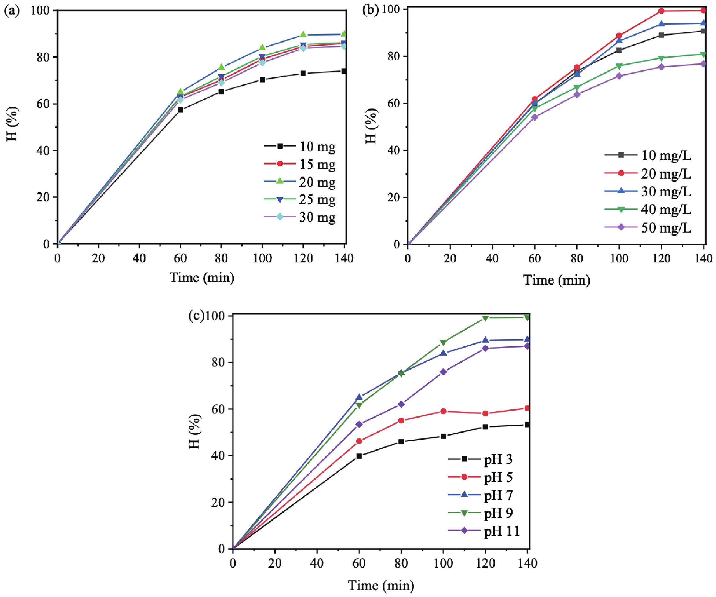
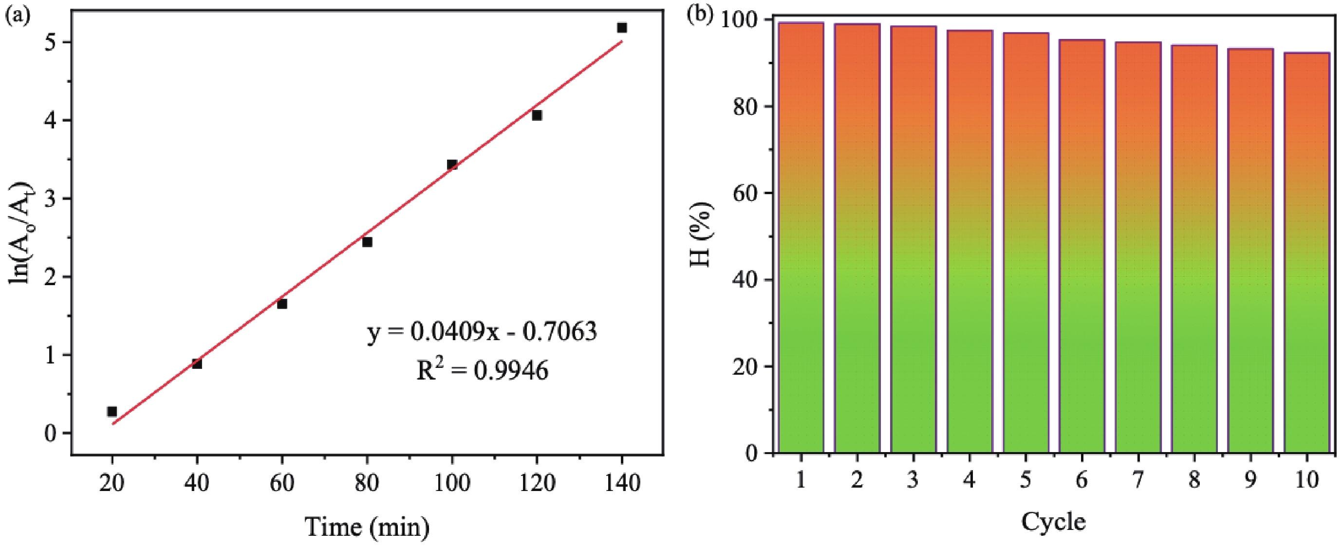
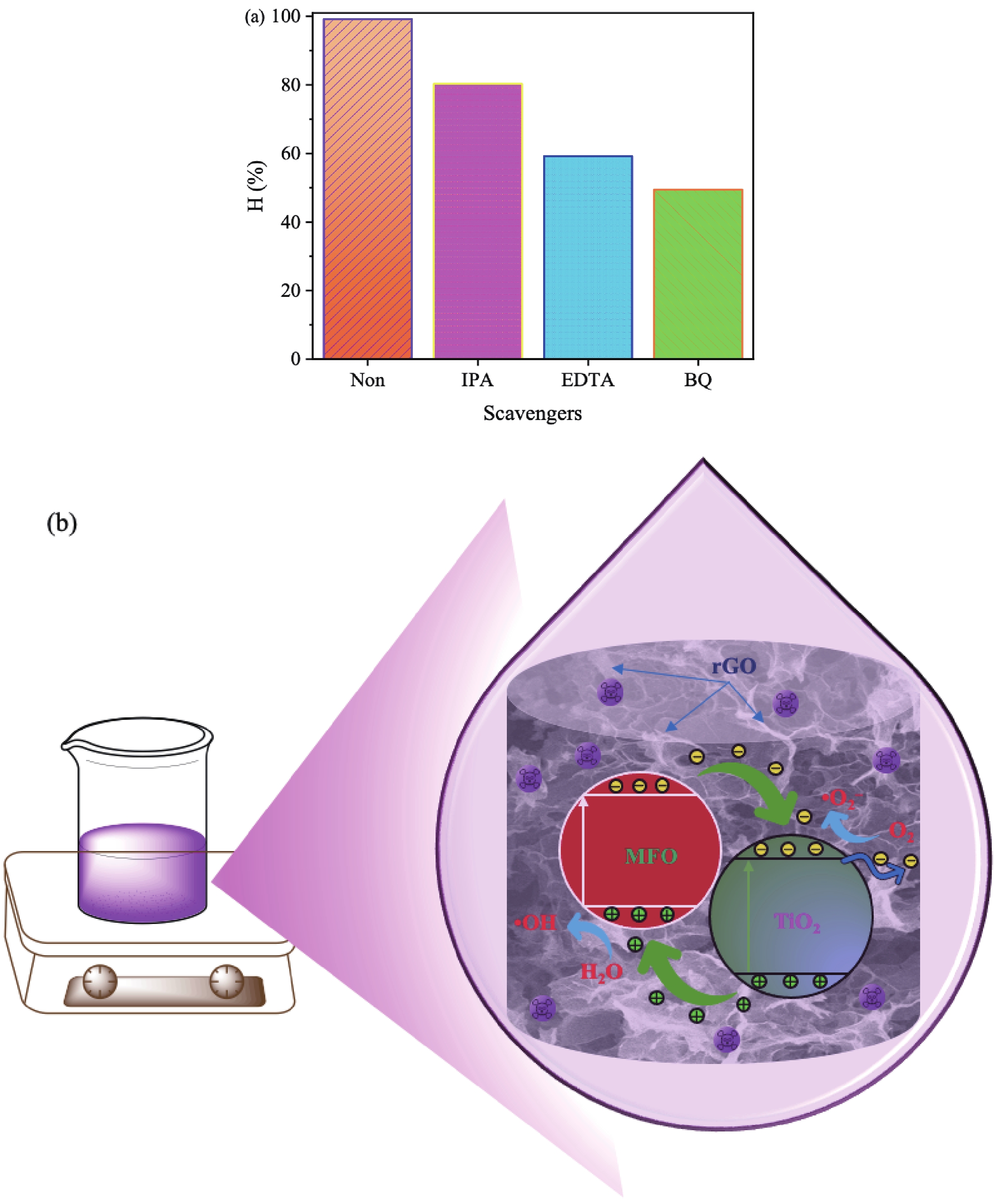
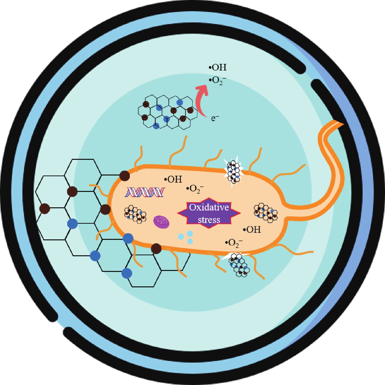
In this study, three-dimensional porous magnesium ferrite/titanium dioxide/reduced graphene oxide (MgFe2O4-GM/TiO2/rGO (MGTG)) was successfully synthesized via green and hydrothermal-supported co-precipitation methods using the extract of Garcinia mangostana (G. mangostana) as a reducing agent. The characterization results indicate the successful formation of the nano/micro MgFe2O4 (MFO) and TiO2 on the structure of the reduced graphene oxide (rGO), which can also act as efficient support, alleviating the agglomeration of the nano/micro MFO and TiO2. The synergic effects of the adsorption and photodegradation activity of the material were investigated according to the removal of crystal violet (CV) under ultraviolet light. The effects of catalyst dosage, CV concentration, and pH on the CV removal efficiency of the MGTG were also investigated. According to the results, the CV photodegradation of the MGTG-200 corresponded to the pseudo-first-order kinetic model. The reusability of the material after 10 cycles also showed a removal efficiency of 92%. This happened because the materials can easily be recollected using external magnets. In addition, according to the effects of different free radicals · O2−, h+, and · OH on the photodegradation process, the photocatalysis mechanism of the MGTG was also thoroughly suggested. The antibacterial efficiency of the MGTG was also evaluated according to the inhibition of the Gram-positive bacteria strain Staphylococcus aureus (S. aureus). Concurrently, the antibacterial mechanism of the fabricated material was also proposed. These results confirm that the prepared material can be potentially employed in a wide range of applications, including wastewater treatment and antibacterial activity.


J. Semicond.
2023, 44(12): 122801 doi: 10.1088/1674-4926/44/12/122801

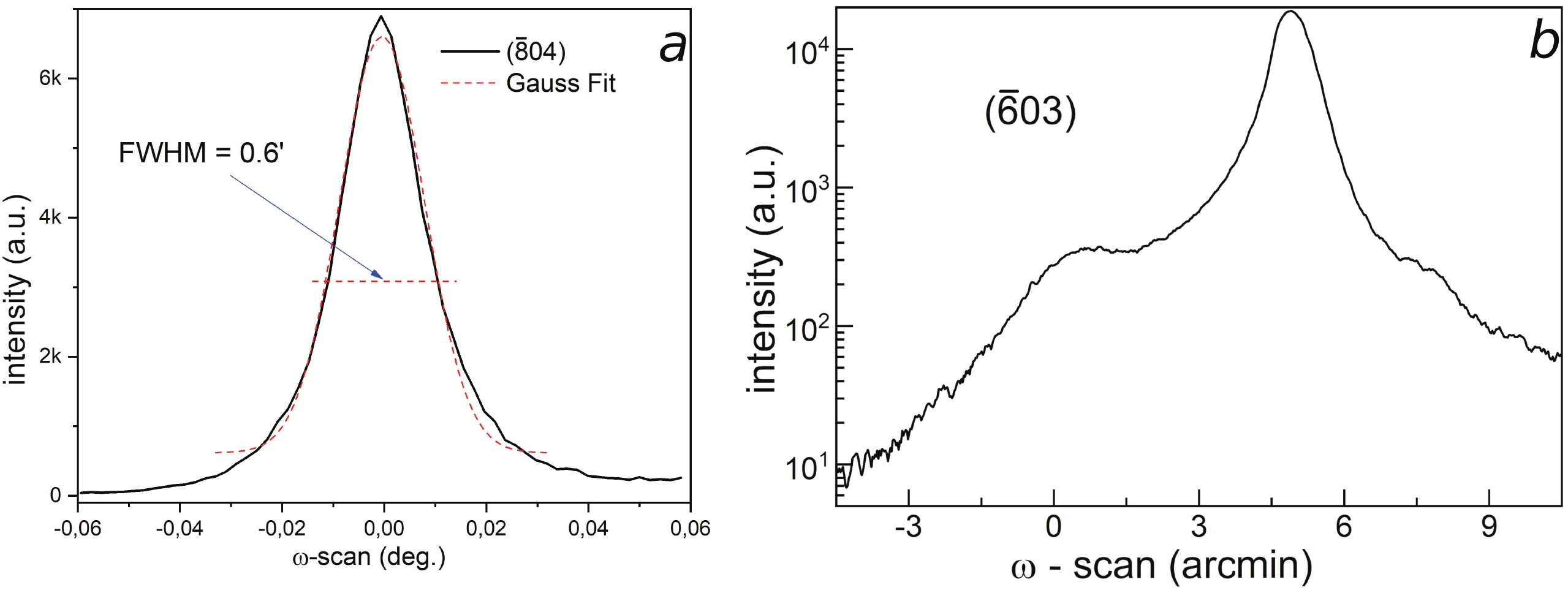
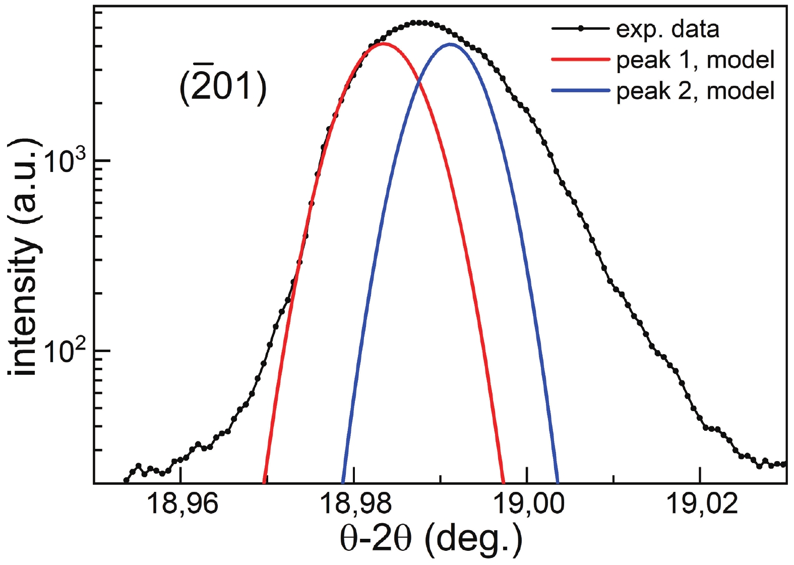
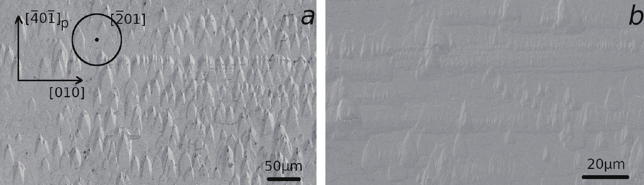
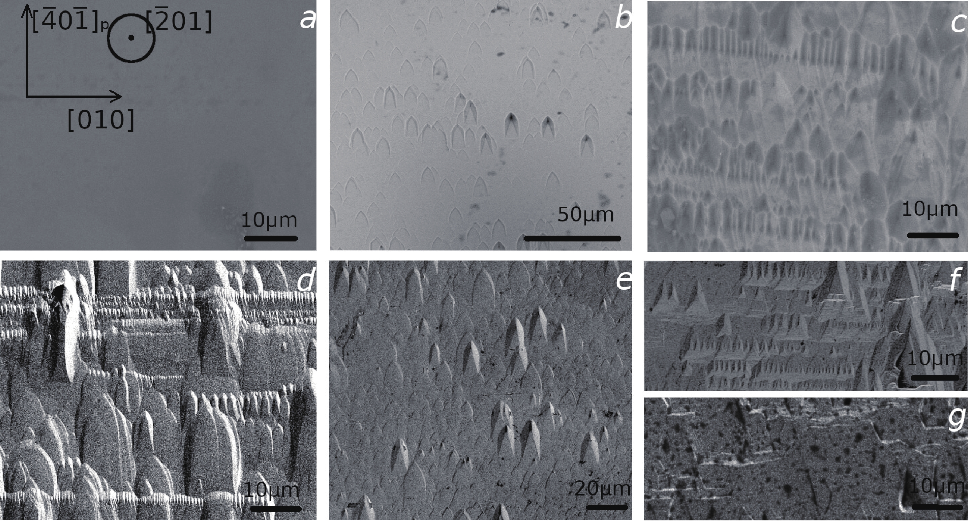
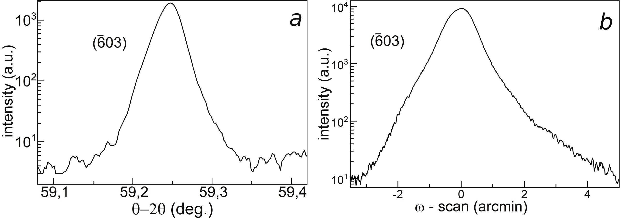
A commercial epi-ready ($ {\bar 2}01 $) β-Ga2O3 wafer was investigated upon diamond sawing into pieces measuring 2.5 × 3 mm2. The defect structure and crystallinity in the cut samples has been studied by X-ray diffraction and a selective wet etching technique. The density of defects was estimated from the average value of etch pits calculated, including near-edge regions, and was obtained close to 109 cm−2. Blocks with lattice orientation deviated by angles of 1−3 arcmin, as well as non-stoichiometric fractions with a relative strain about (1.0−1.5) × 10−4 in the [$ {\bar 2}01 $] direction, were found. Crystal perfection was shown to decrease significantly towards the cutting lines of the samples. To reduce the number of structural defects and increase the crystal perfection of the samples via increasing defect motion mobility, the thermal annealing was employed. Polygonization and formation of a mosaic structure coupled with dislocation wall appearance upon 3 h of annealing at 1100 °C was observed. The fractions characterized by non-stoichiometry phases and the block deviation disappeared. The annealing for 11 h improved the homogeneity and perfection in the crystals. The average density of the etch pits dropped down significantly to 8 × 106 cm−2.


J. Semicond.
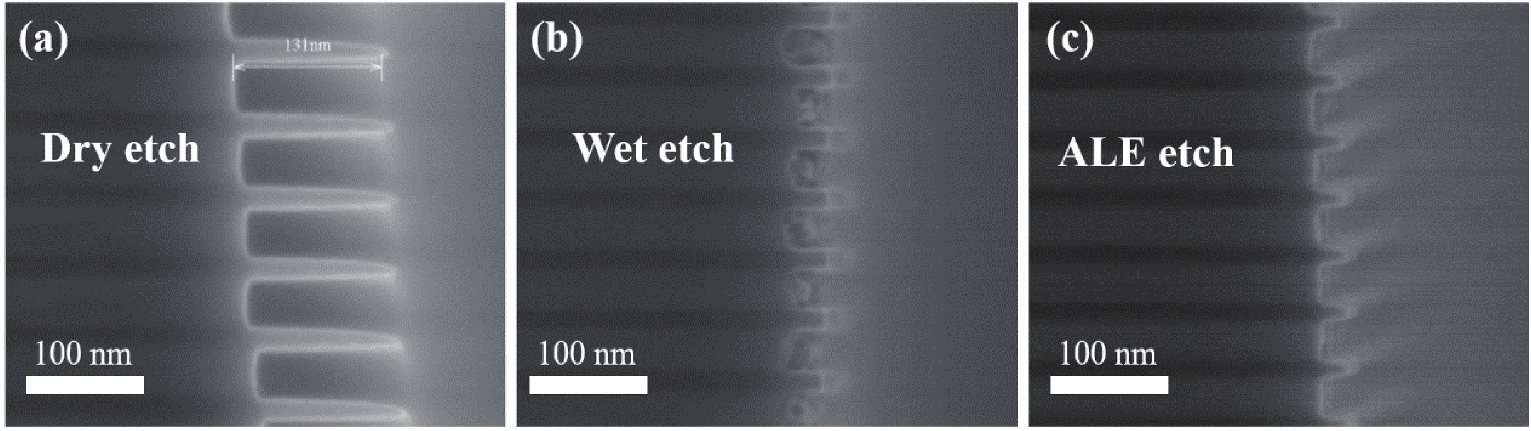
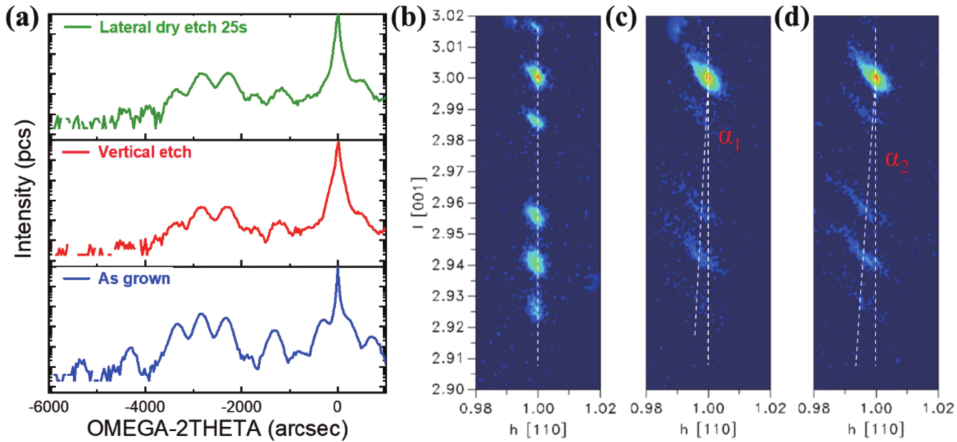
2023, 44(12): 124101 doi: 10.1088/1674-4926/44/12/124101
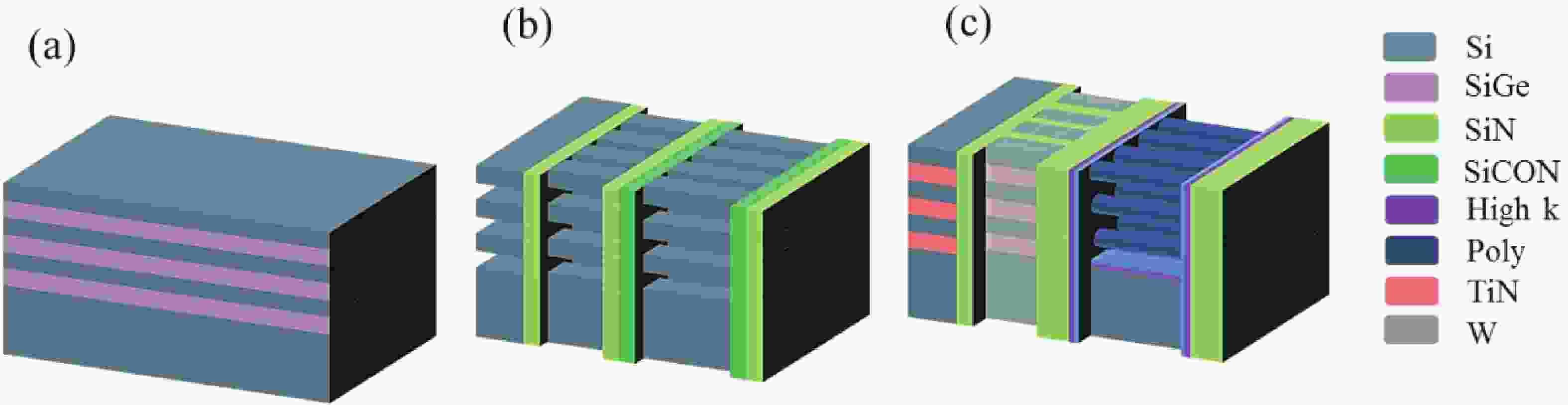
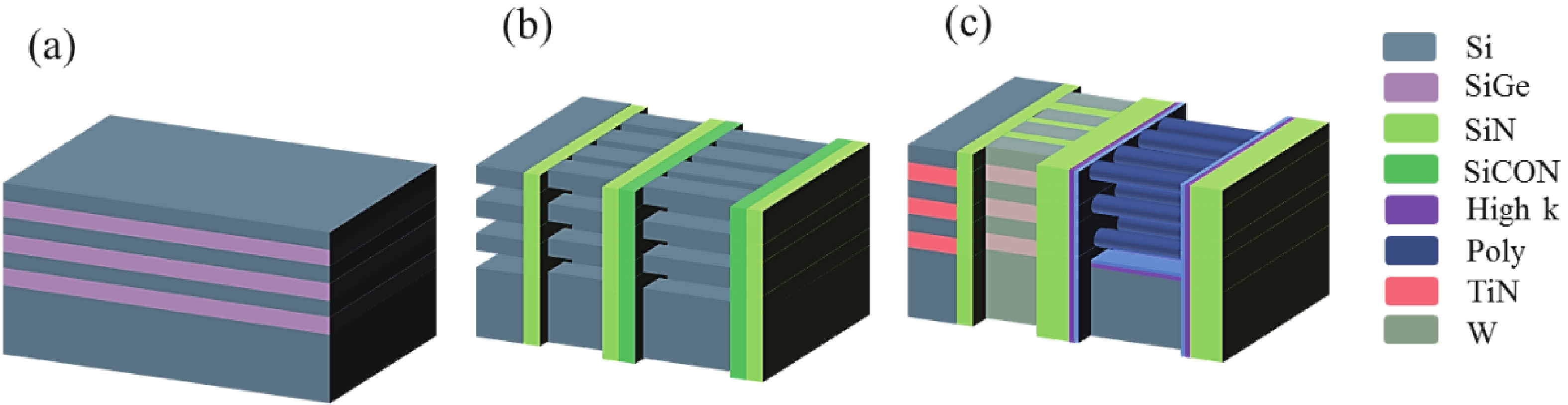
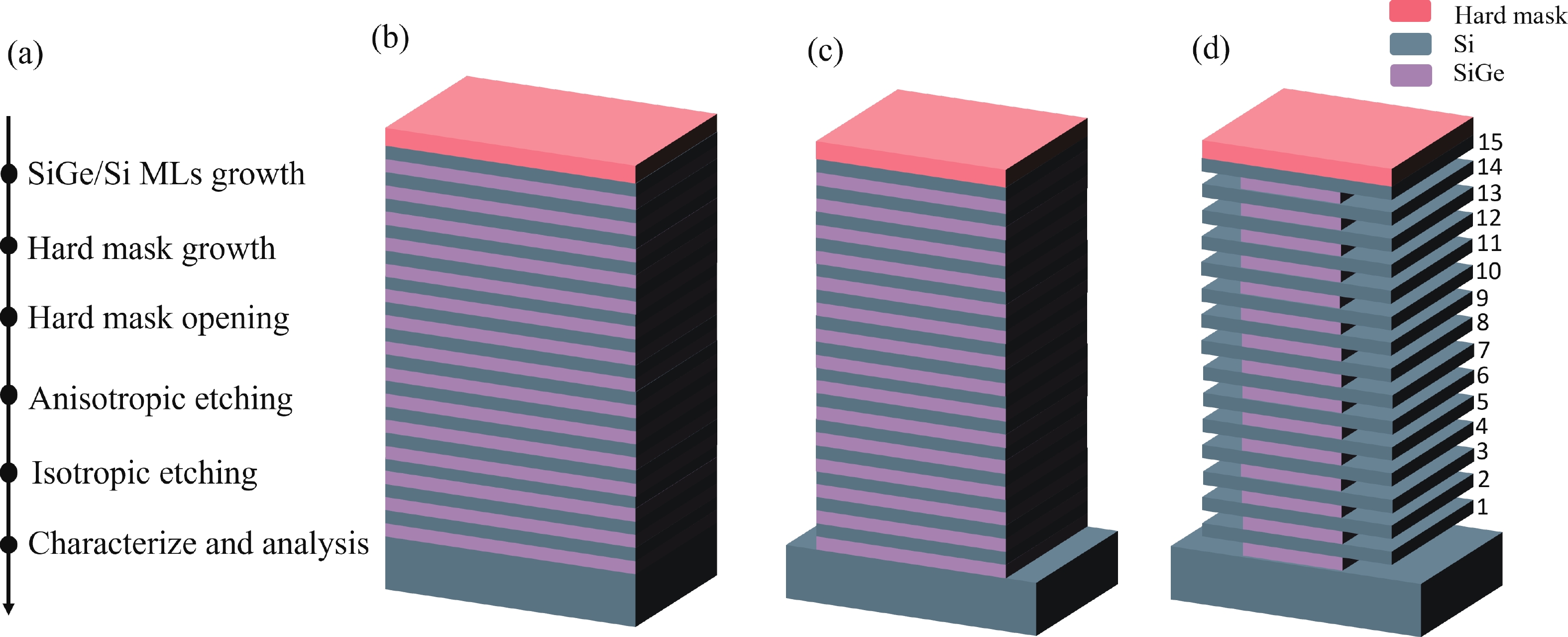
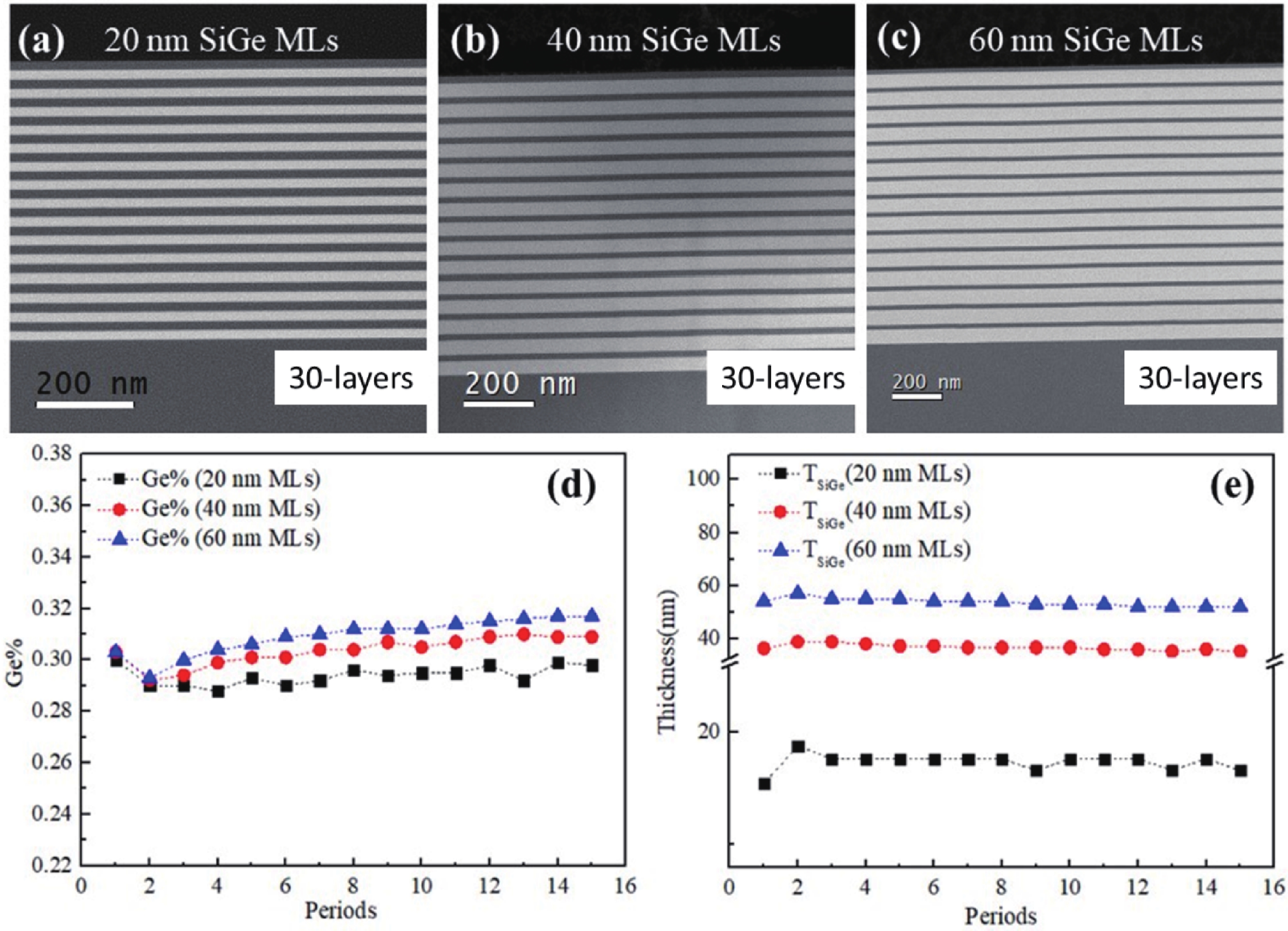
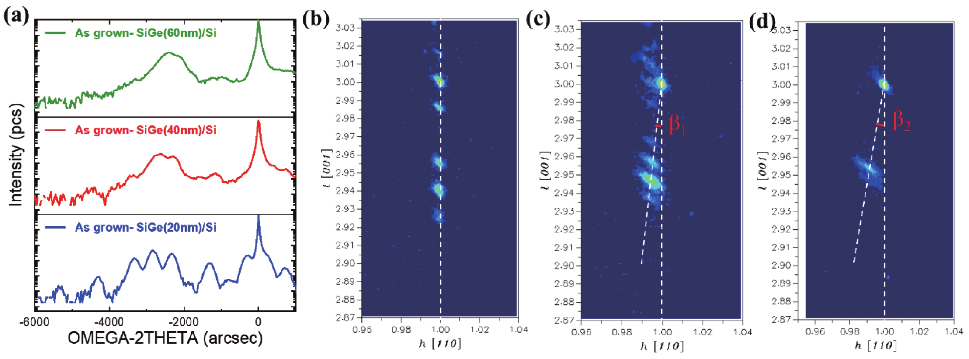
Fifteen periods of Si/Si0.7Ge0.3 multilayers (MLs) with various SiGe thicknesses are grown on a 200 mm Si substrate using reduced pressure chemical vapor deposition (RPCVD). Several methods were utilized to characterize and analyze the ML structures. The high resolution transmission electron microscopy (HRTEM) results show that the ML structure with 20 nm Si0.7Ge0.3 features the best crystal quality and no defects are observed. Stacked Si0.7Ge0.3 ML structures etched by three different methods were carried out and compared, and the results show that they have different selectivities and morphologies. In this work, the fabrication process influences on Si/SiGe MLs are studied and there are no significant effects on the Si layers, which are the channels in lateral gate all around field effect transistor (L-GAAFET) devices. For vertically-stacked dynamic random access memory (VS-DRAM), it is necessary to consider the dislocation caused by strain accumulation and stress release after the number of stacked layers exceeds the critical thickness. These results pave the way for the manufacture of high-performance multivertical-stacked Si nanowires, nanosheet L-GAAFETs, and DRAM devices.