Issue Browser
Volume 44, Issue 3,
Mar 2023


J. Semicond.
2023, 44(3): 031001 doi: 10.1088/1674-4926/44/3/031001
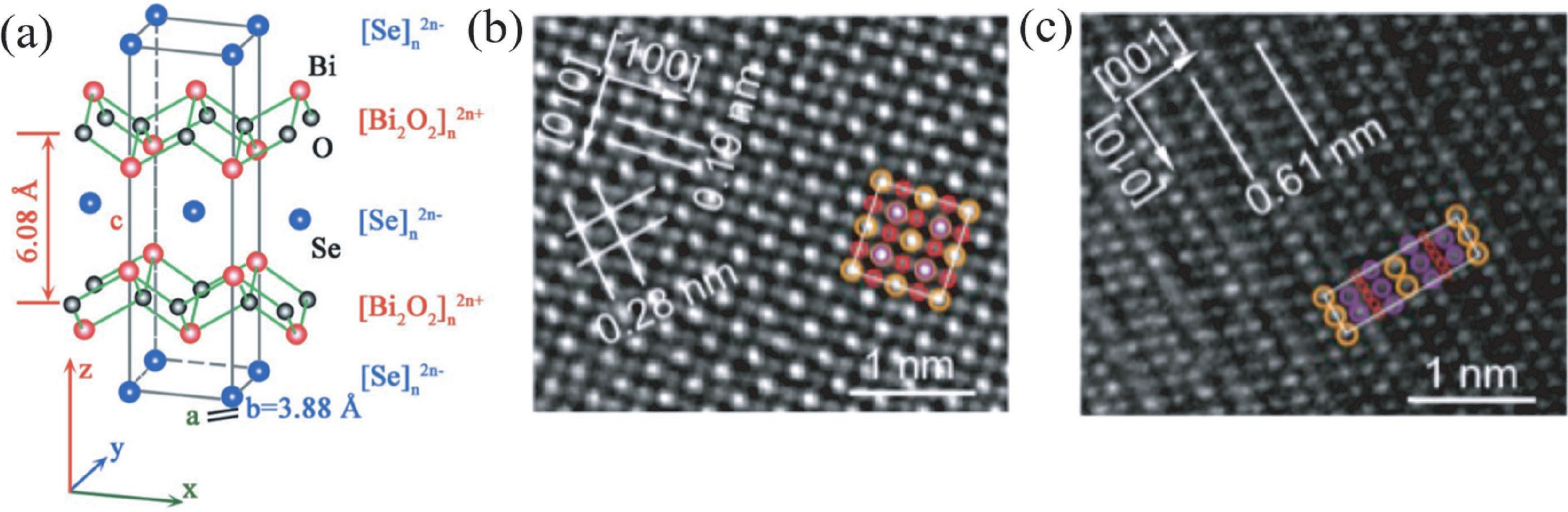
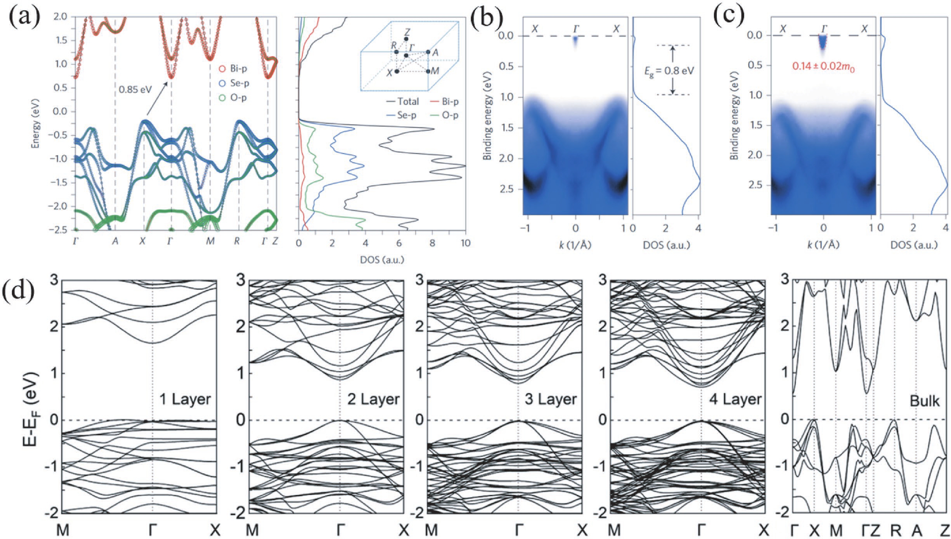
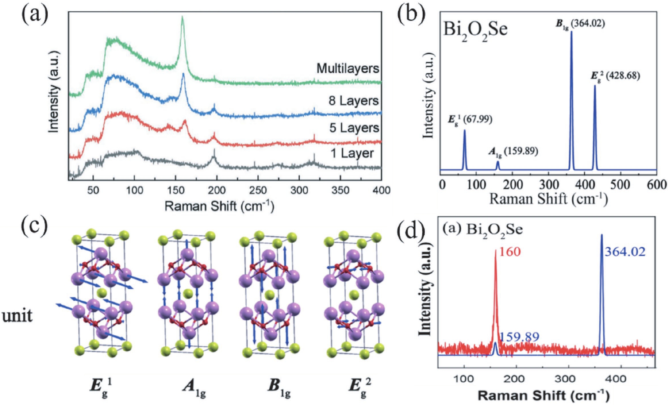
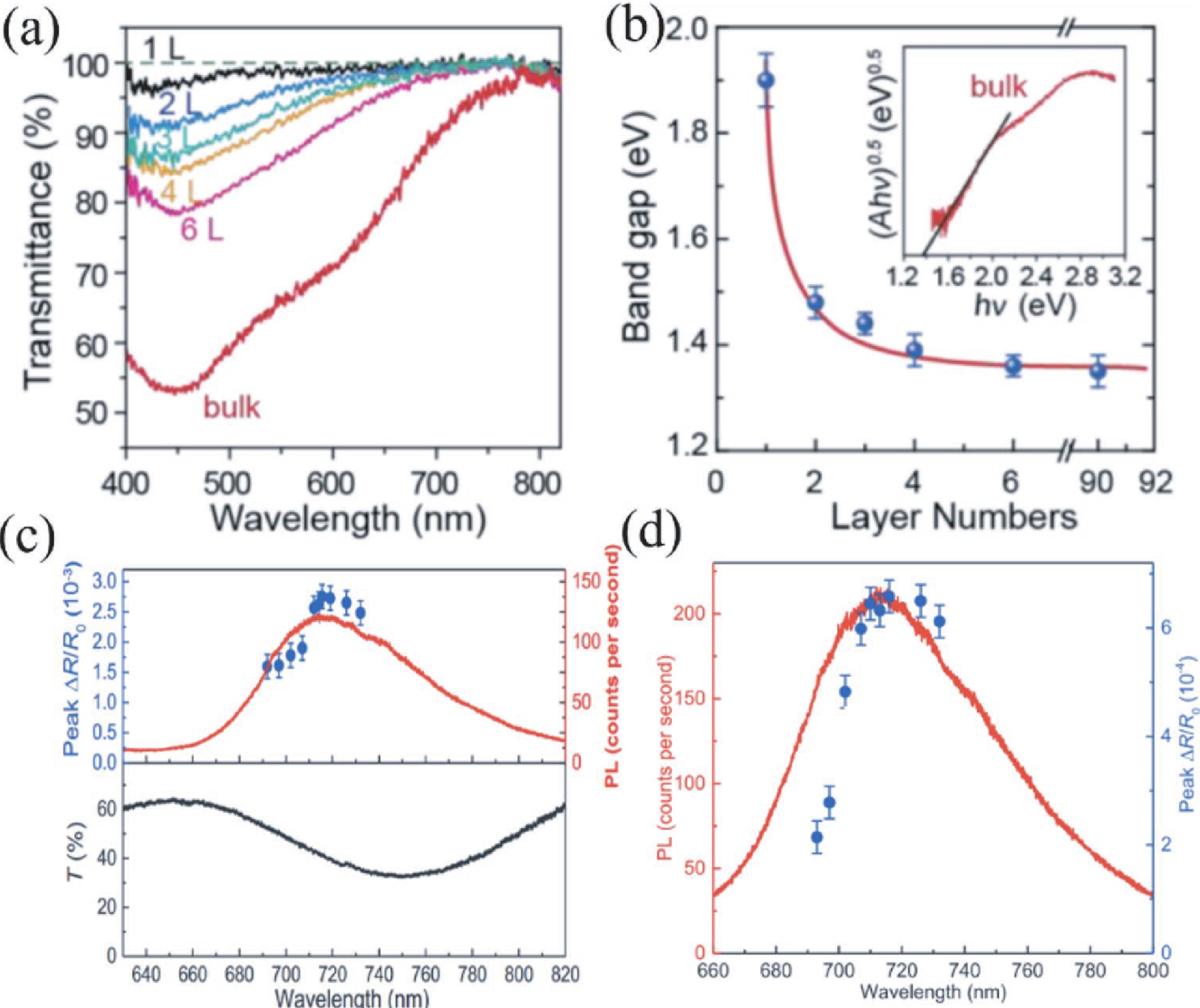
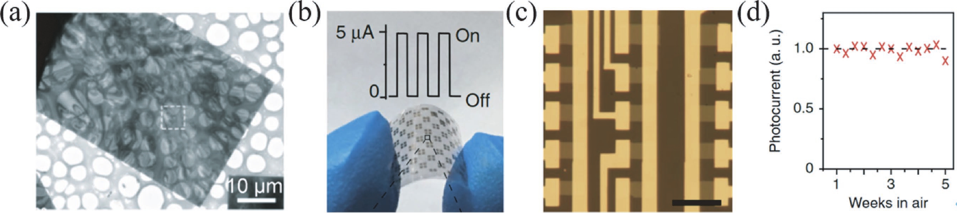
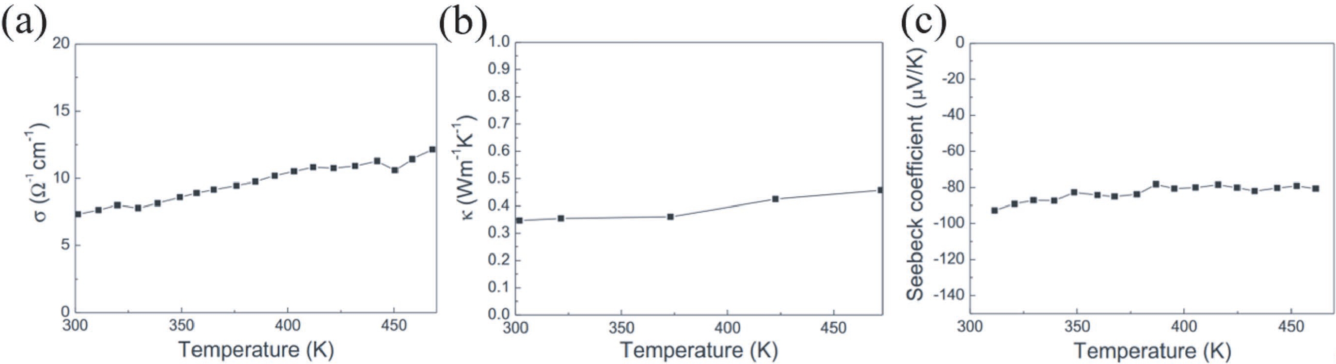
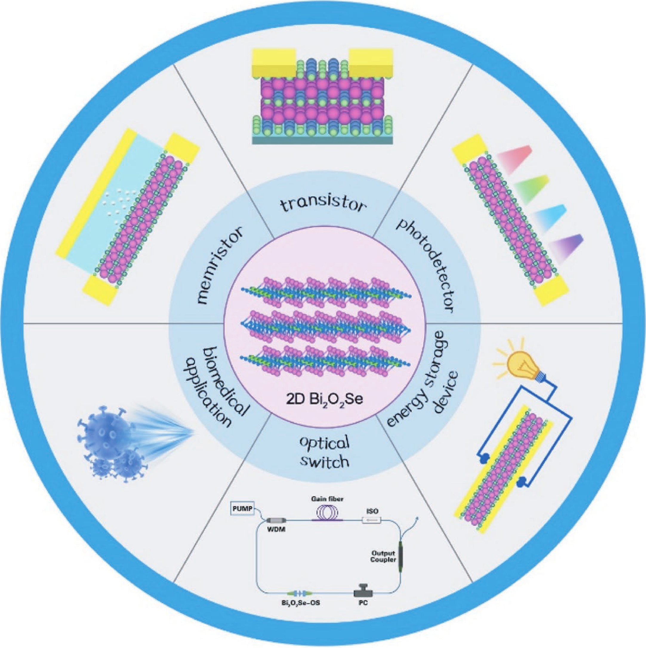
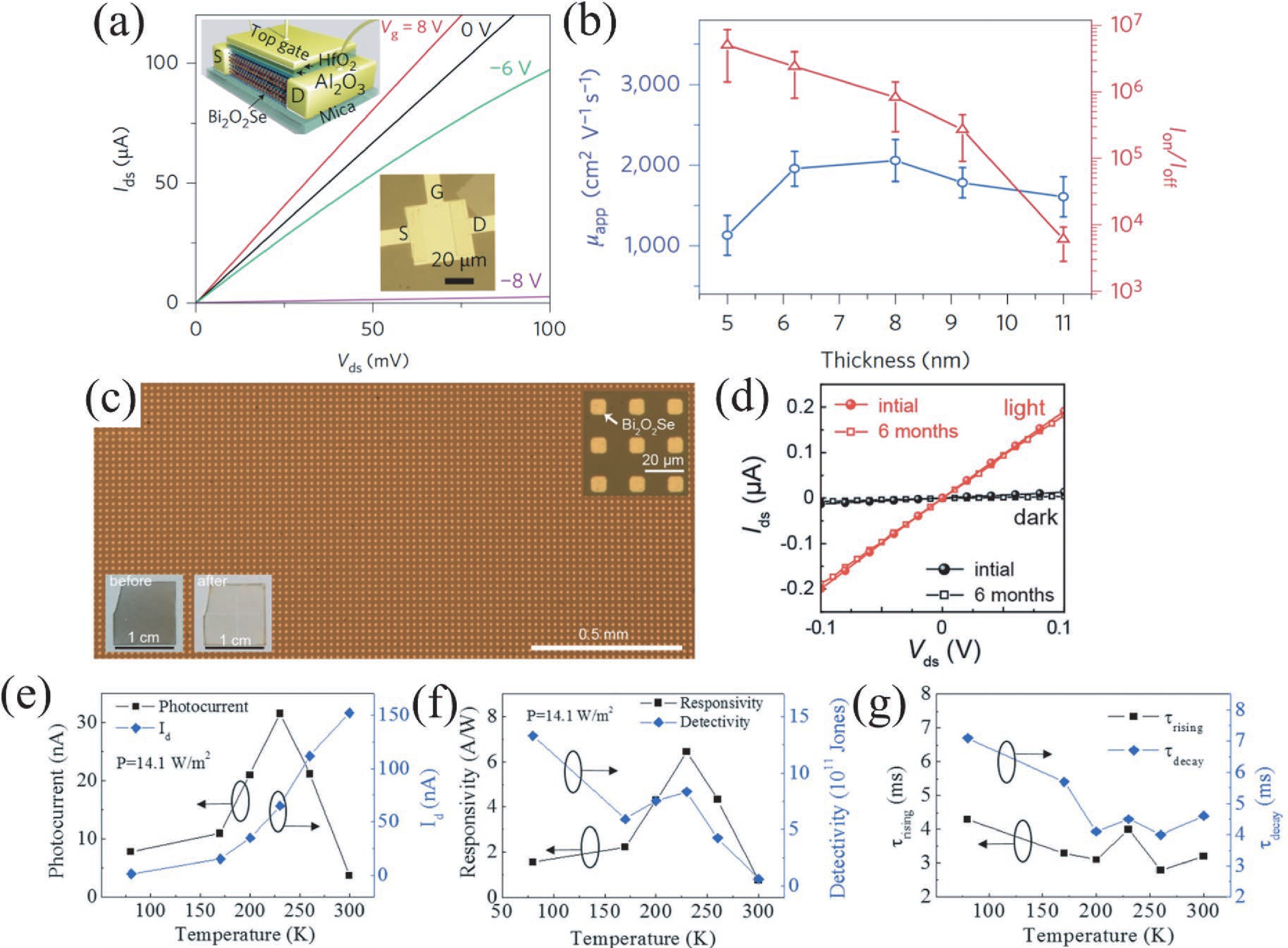
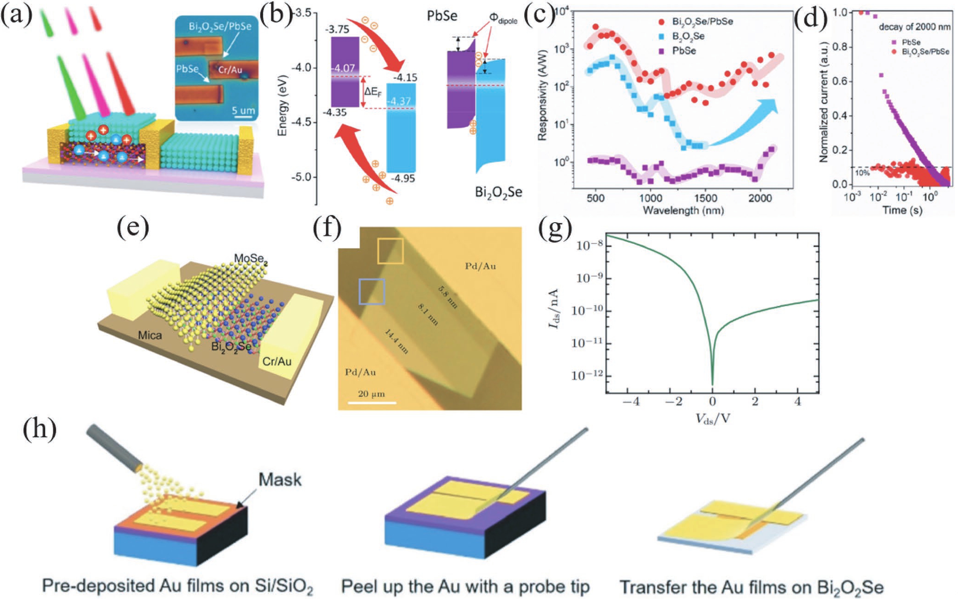
Two-dimensional materials have shown great application potential in high-performance electronic devices because they are ultrathin, have an ultra-large specific surface area, high carrier mobility, efficient channel current regulation, and extraordinary integration. In addition to graphene, other types of 2D nanomaterials have also been studied and applied in photodetectors, solar cells, energy storage devices, and so on. Bi2O2Se is an emerging 2D semiconductor material with very high electron mobility, modest bandgap, near-ideal subthreshold swing, and excellent thermal and chemical stability. Even in a monolayer structure, Bi2O2Se has still exhibited efficient light absorption. In this mini review, the latest main research progresses on the preparation methods, electric structure, and the optical, mechanical, and thermoelectric properties of Bi2O2Se are summarized. The wide rang of applications in electronics and photoelectronic devices are then reviewed. This review concludes with a discussion of the existing open questions/challenges and future prospects for Bi2O2Se.

J. Semicond.
2023, 44(3): 031701 doi: 10.1088/1674-4926/44/3/031701
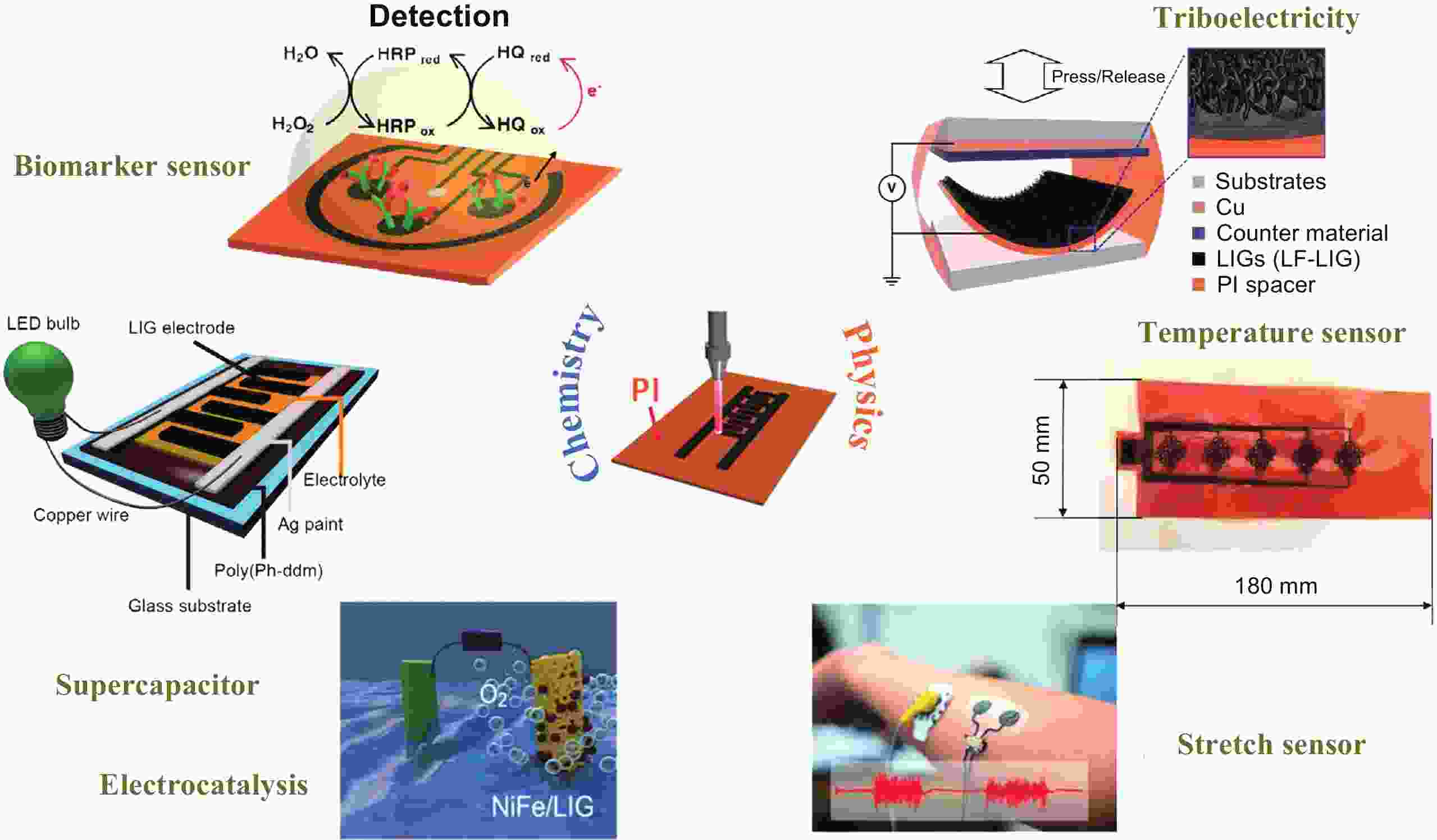
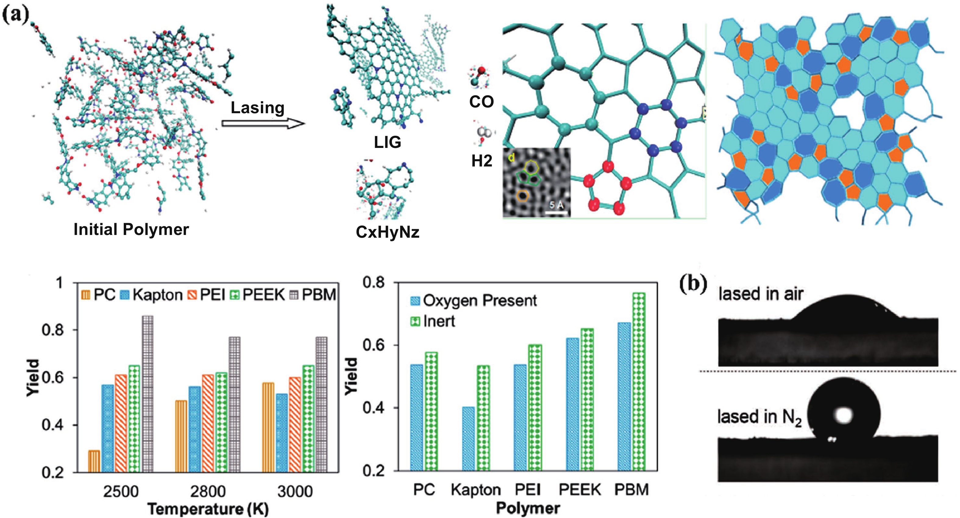
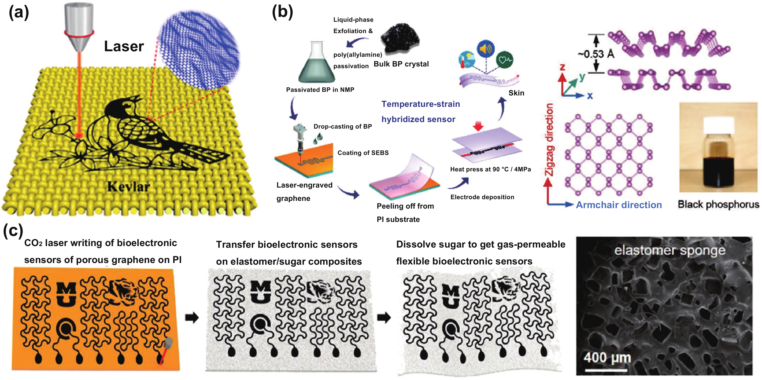
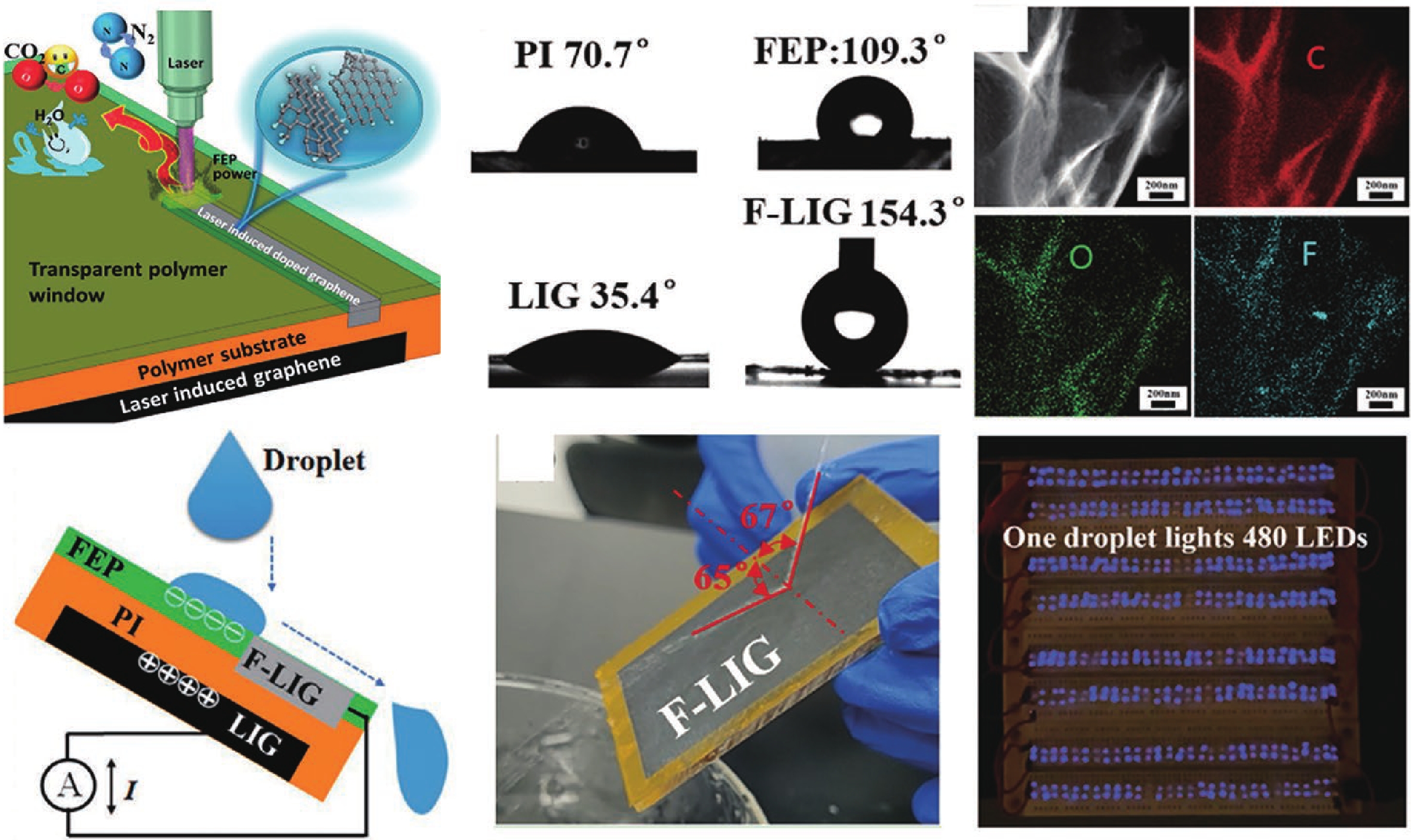
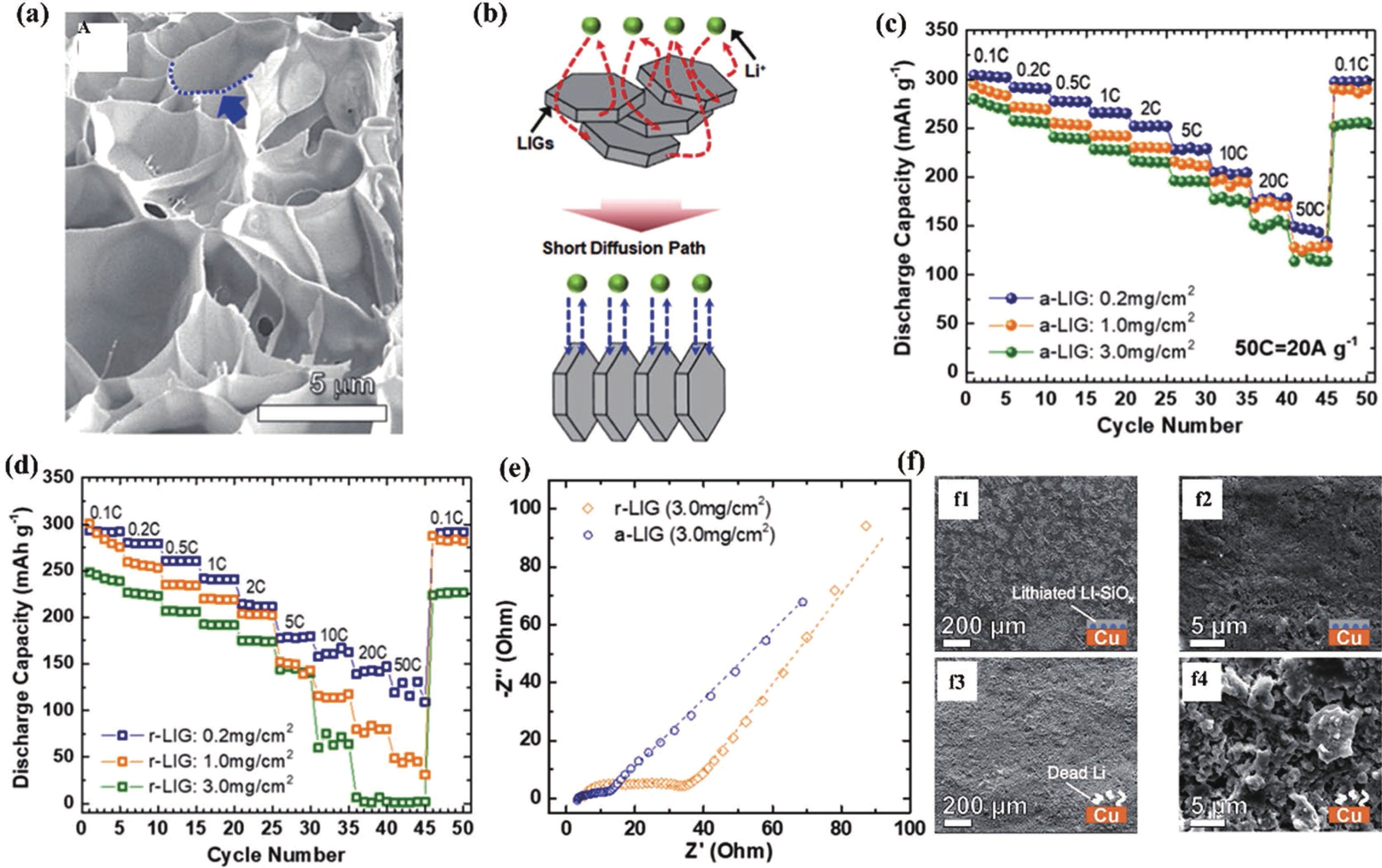
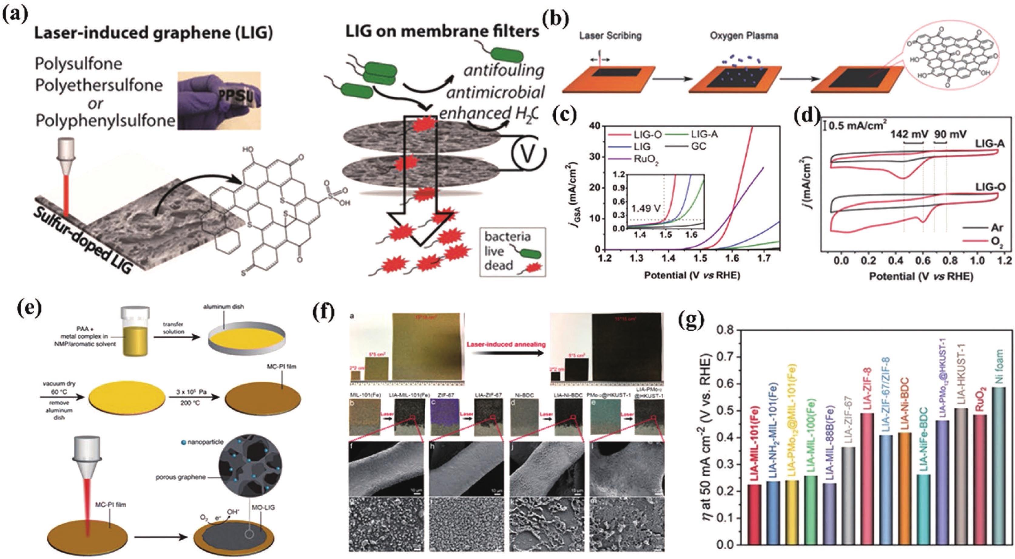
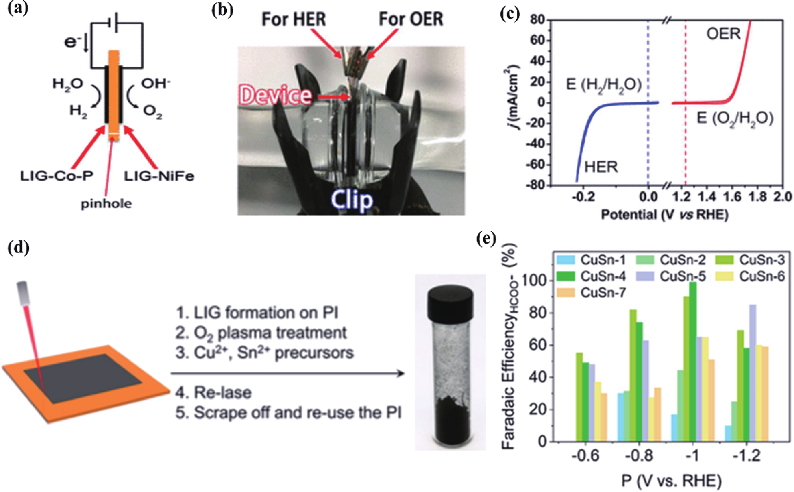
Laser writing is a fast and efficient technology that can produce graphene with a high surface area, whereas laser-induced graphene (LIG) has been widely used in both physics and chemical device application. It is necessary to update this important progress because it may provide a clue to consider the current challenges and possible future directions. In this review, the basic principles of LIG fabrication are first briefly described for a detailed understanding of the lasing process. Subsequently, we summarize the physical device applications of LIGs and describe their advantages, including flexible electronics and energy harvesting. Then, chemical device applications are categorized into chemical sensors, supercapacitors, batteries, and electrocatalysis, and a detailed interpretation is provided. Finally, we present our vision of future developments and challenges in this exciting research field.

J. Semicond.
2023, 44(3): 032001 doi: 10.1088/1674-4926/44/3/032001

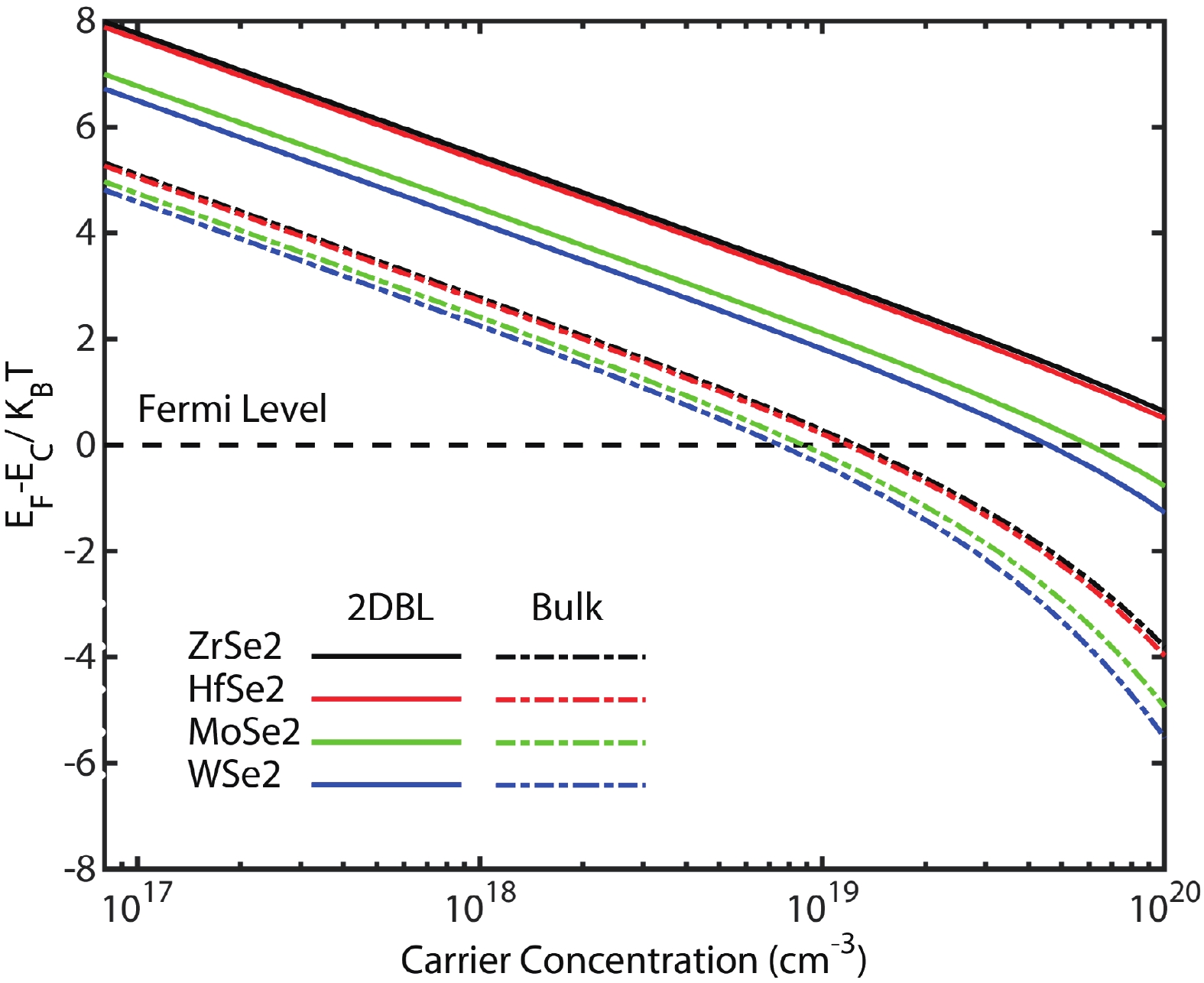
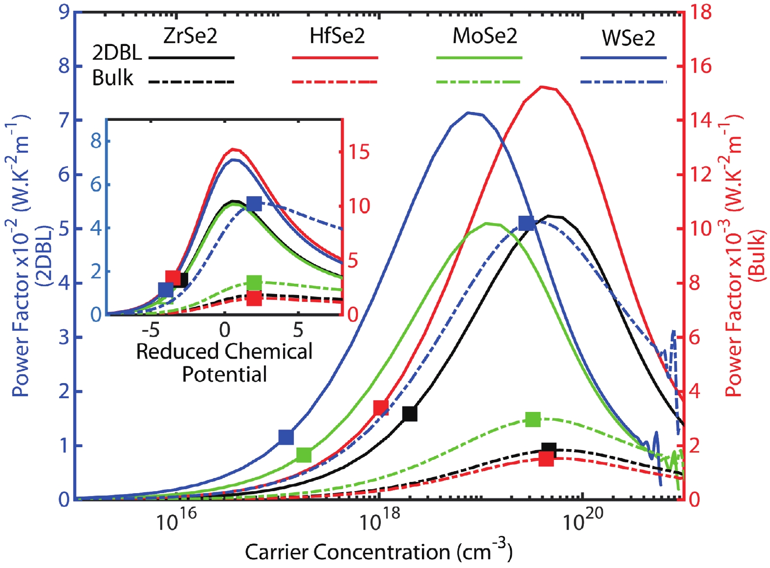
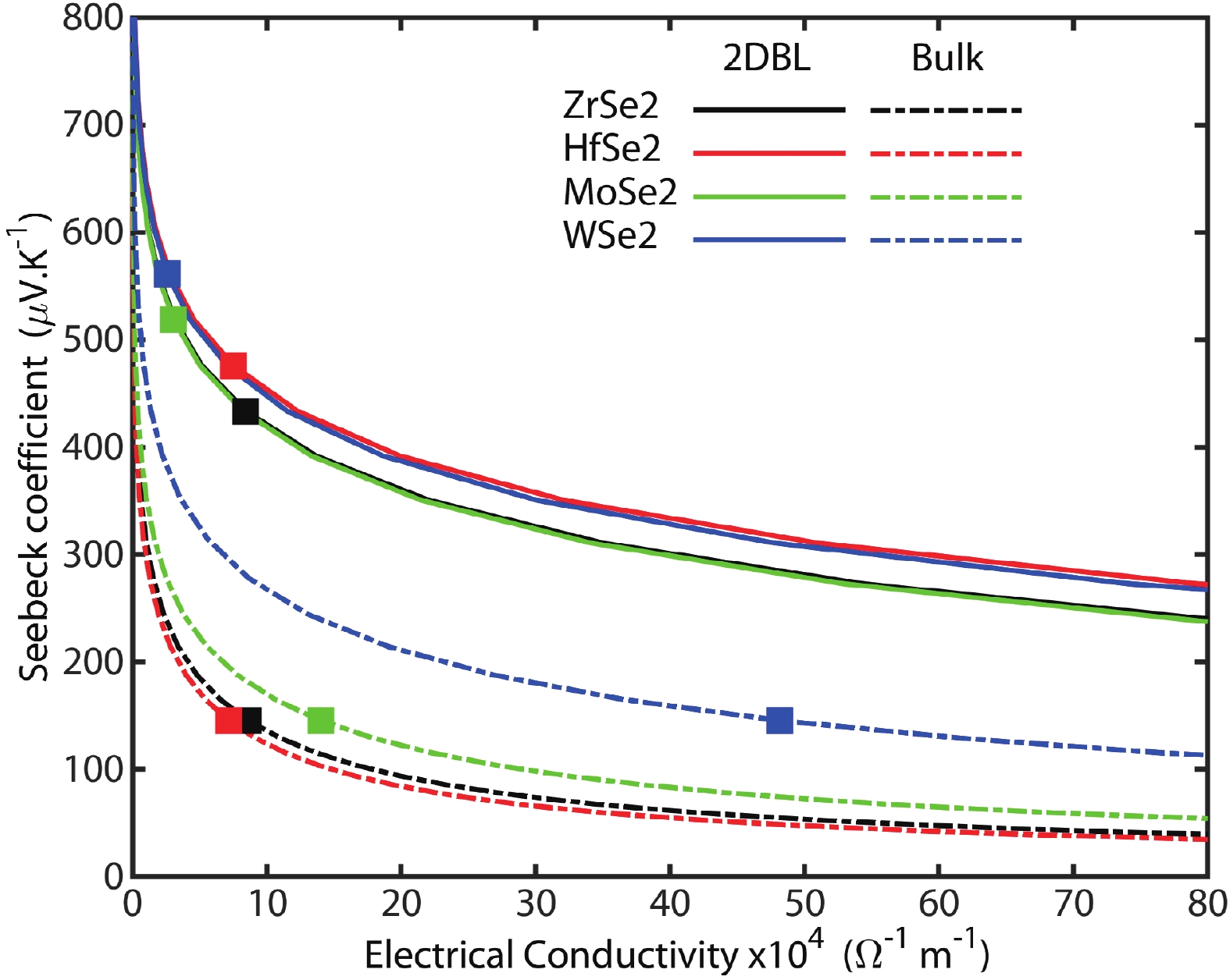
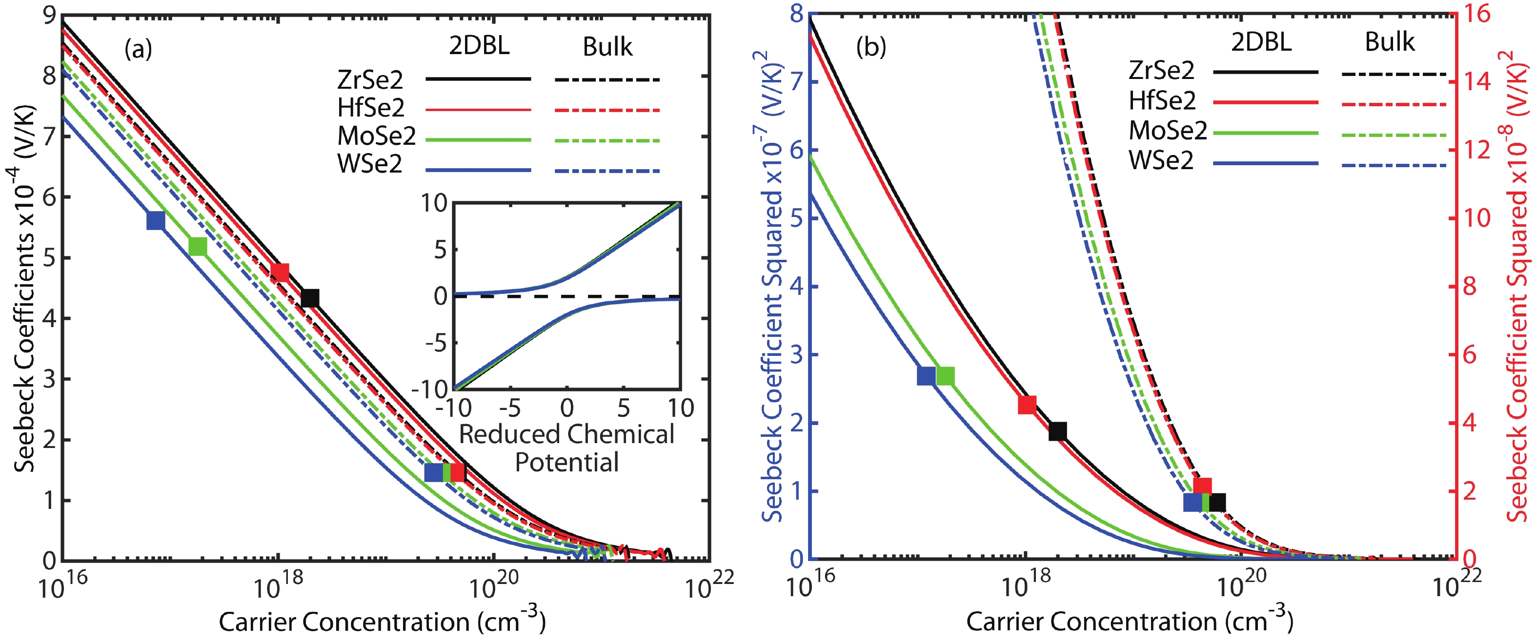
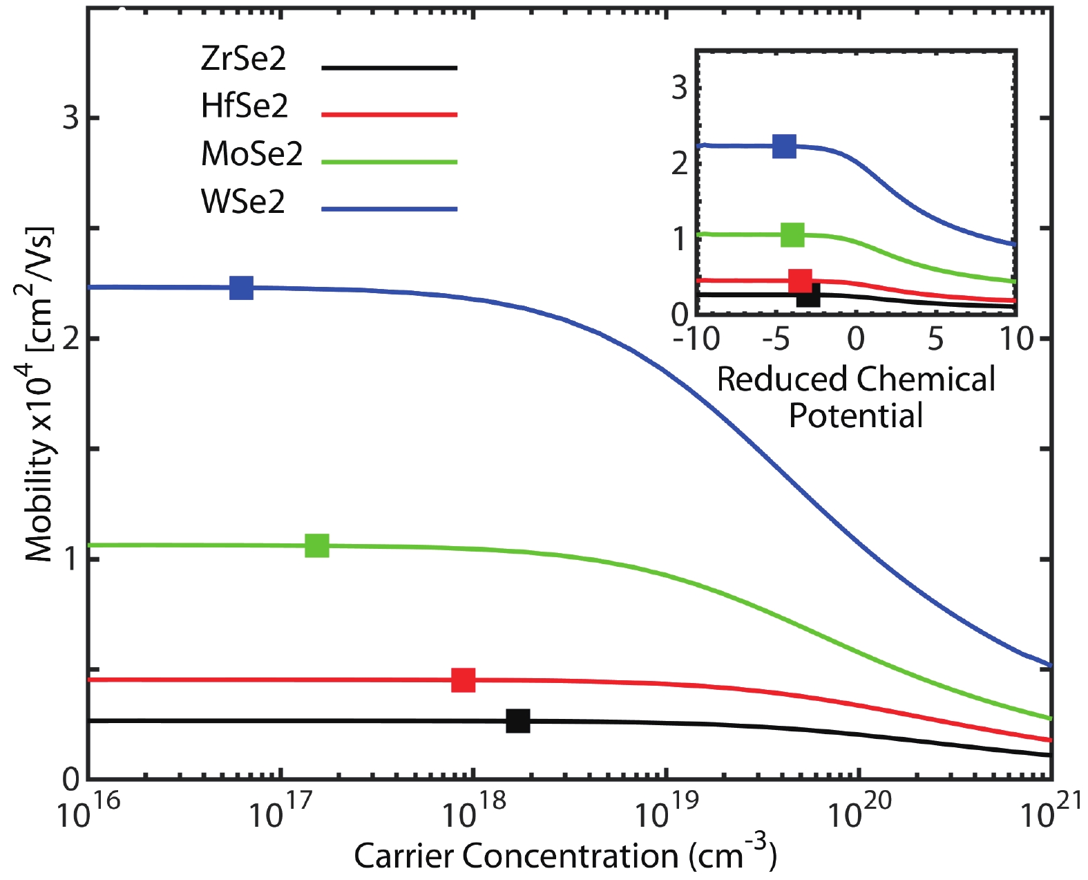
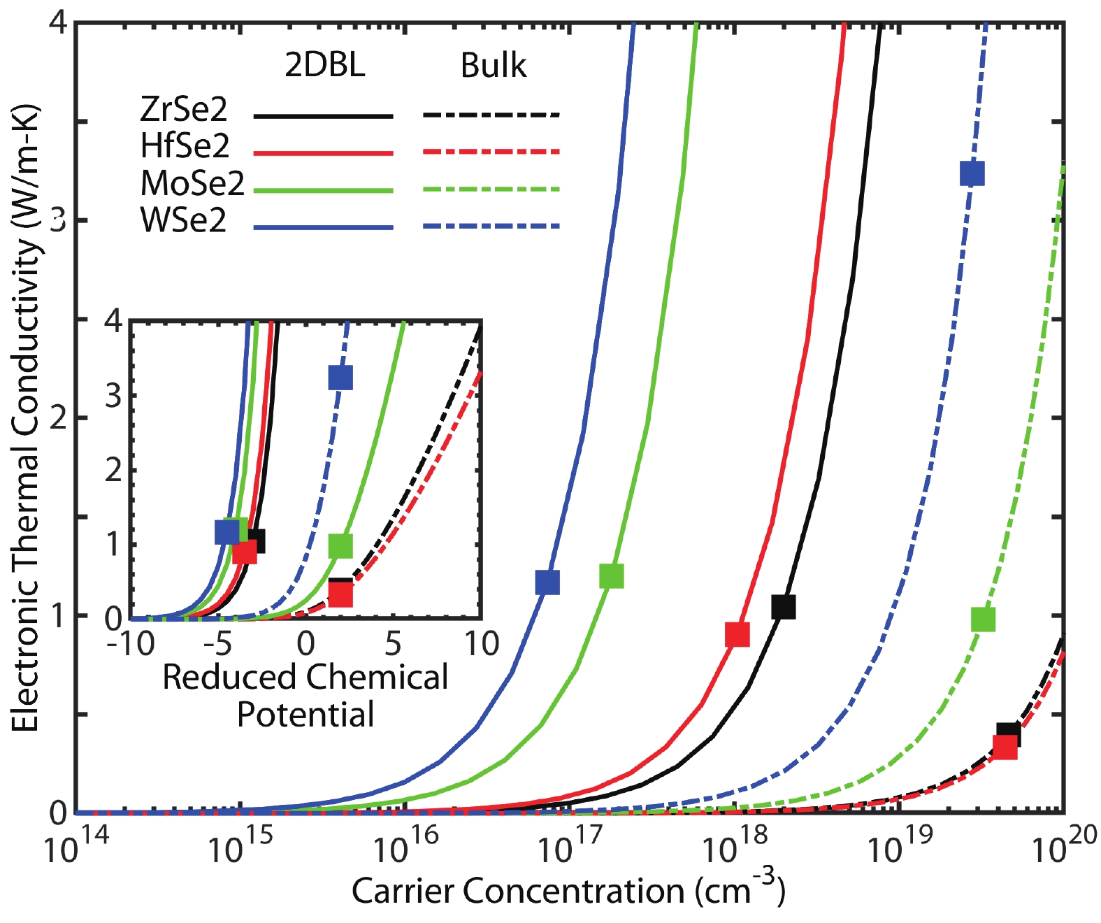
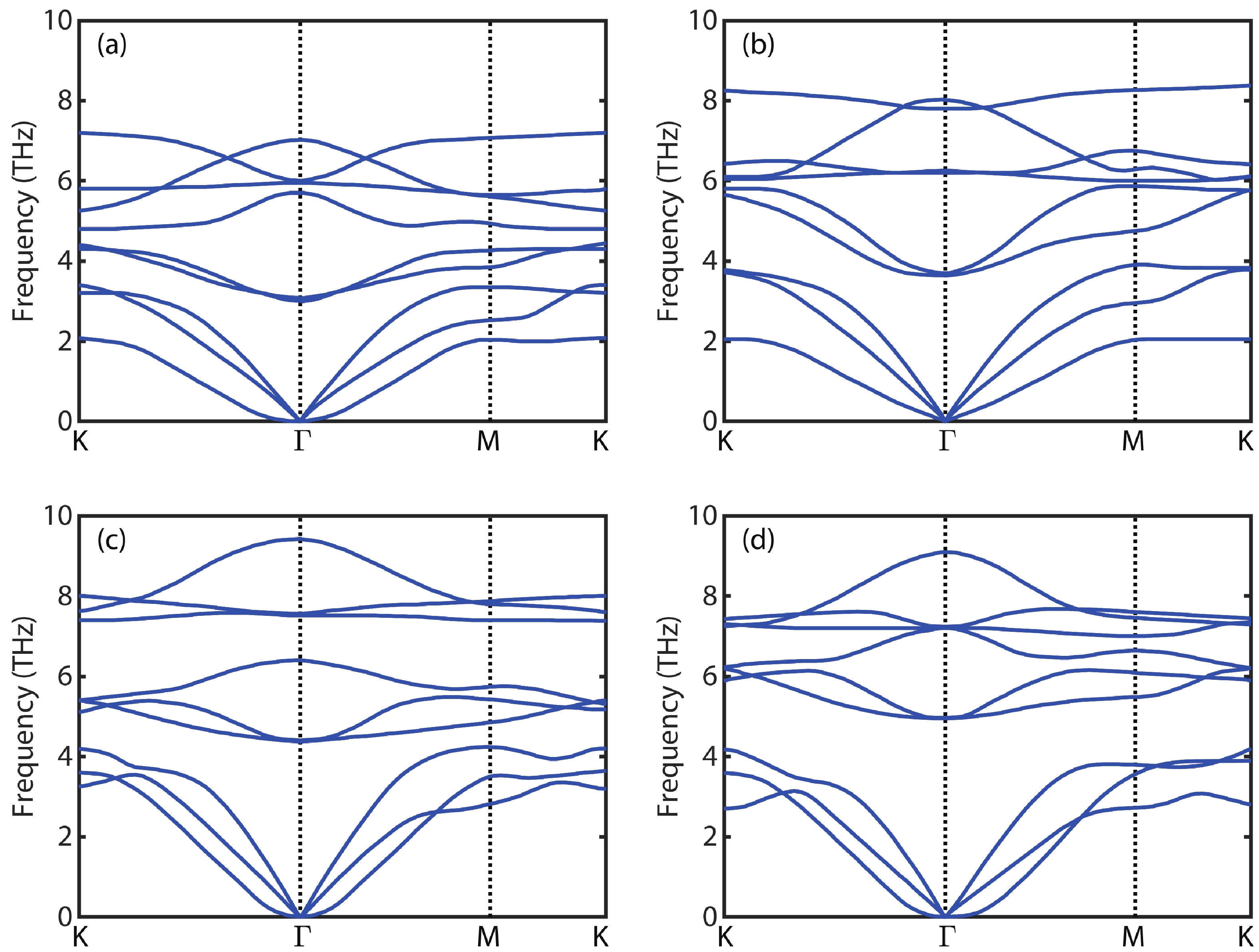
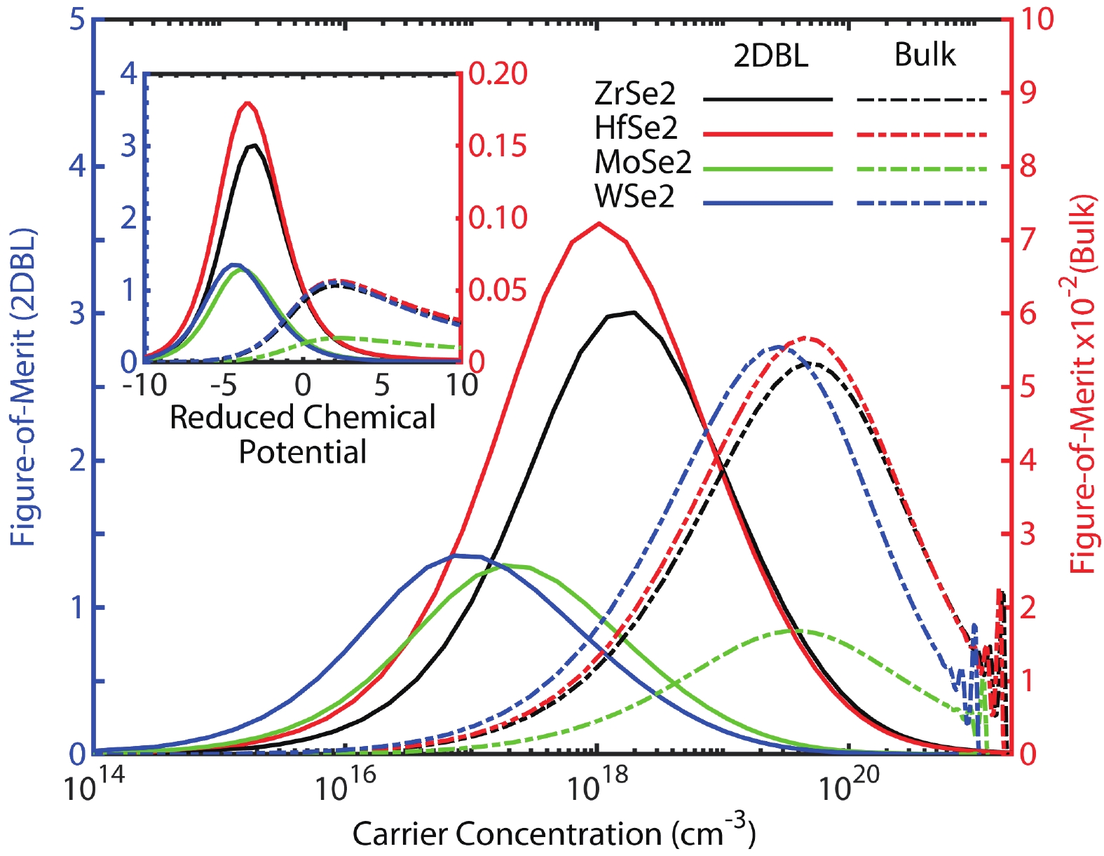
Significant advancements in nanoscale material efficiency optimization have made it feasible to substantially adjust the thermoelectric transport characteristics of materials. Motivated by the prediction and enhanced understanding of the behavior of two-dimensional (2D) bilayers (BL) of zirconium diselenide (ZrSe2), hafnium diselenide (HfSe2), molybdenum diselenide (MoSe2), and tungsten diselenide (WSe2), we investigated the thermoelectric transport properties using information generated from experimental measurements to provide inputs to work with the functions of these materials and to determine the critical factor in the trade-off between thermoelectric materials. Based on the Boltzmann transport equation (BTE) and Barden-Shockley deformation potential (DP) theory, we carried out a series of investigative calculations related to the thermoelectric properties and characterization of these materials. The calculated dimensionless figure of merit (ZT) values of 2DBL-MSe2 (M = Zr, Hf, Mo, W) at room temperature were 3.007, 3.611, 1.287, and 1.353, respectively, with convenient electronic densities. In addition, the power factor is not critical in the trade-off between thermoelectric materials but it can indicate a good thermoelectric performance. Thus, the overall thermal conductivity and power factor must be considered to determine the preference of thermoelectric materials.

J. Semicond.
2023, 44(3): 032201 doi: 10.1088/1674-4926/44/3/032201
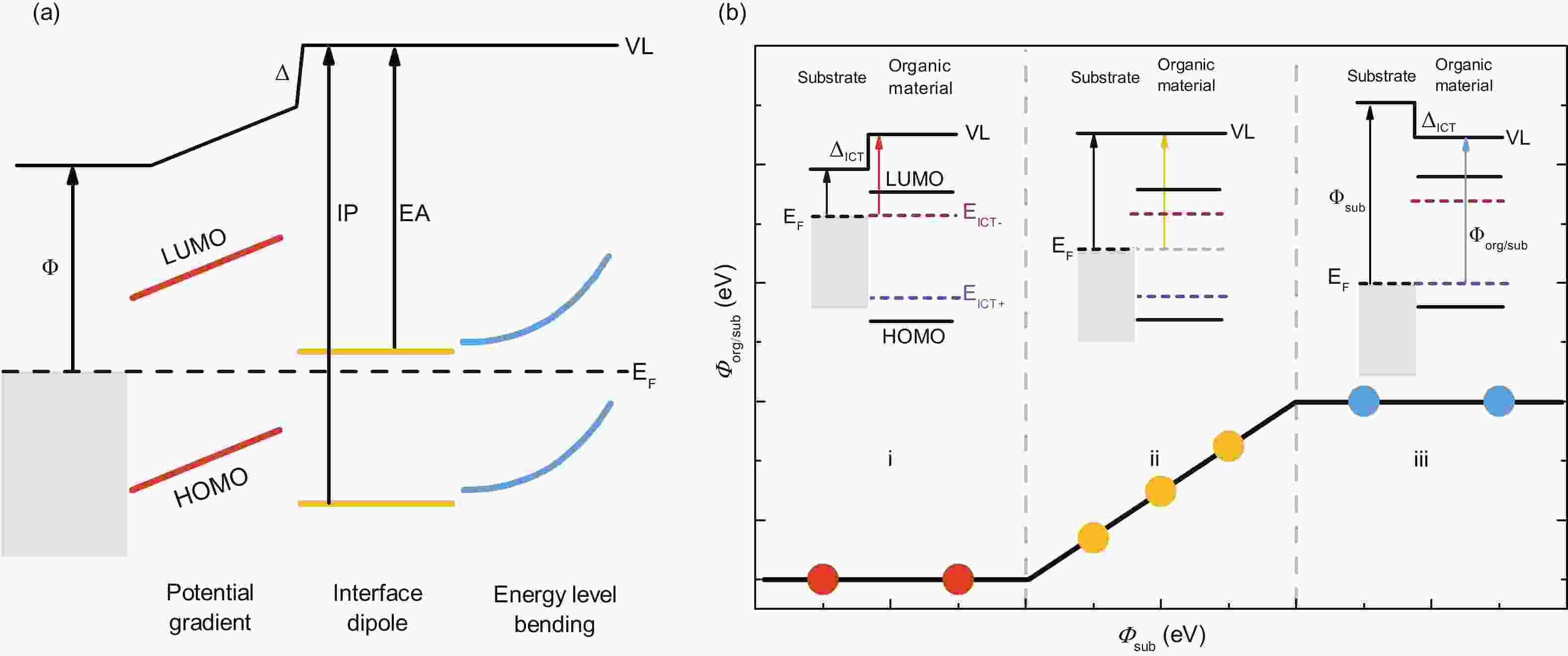
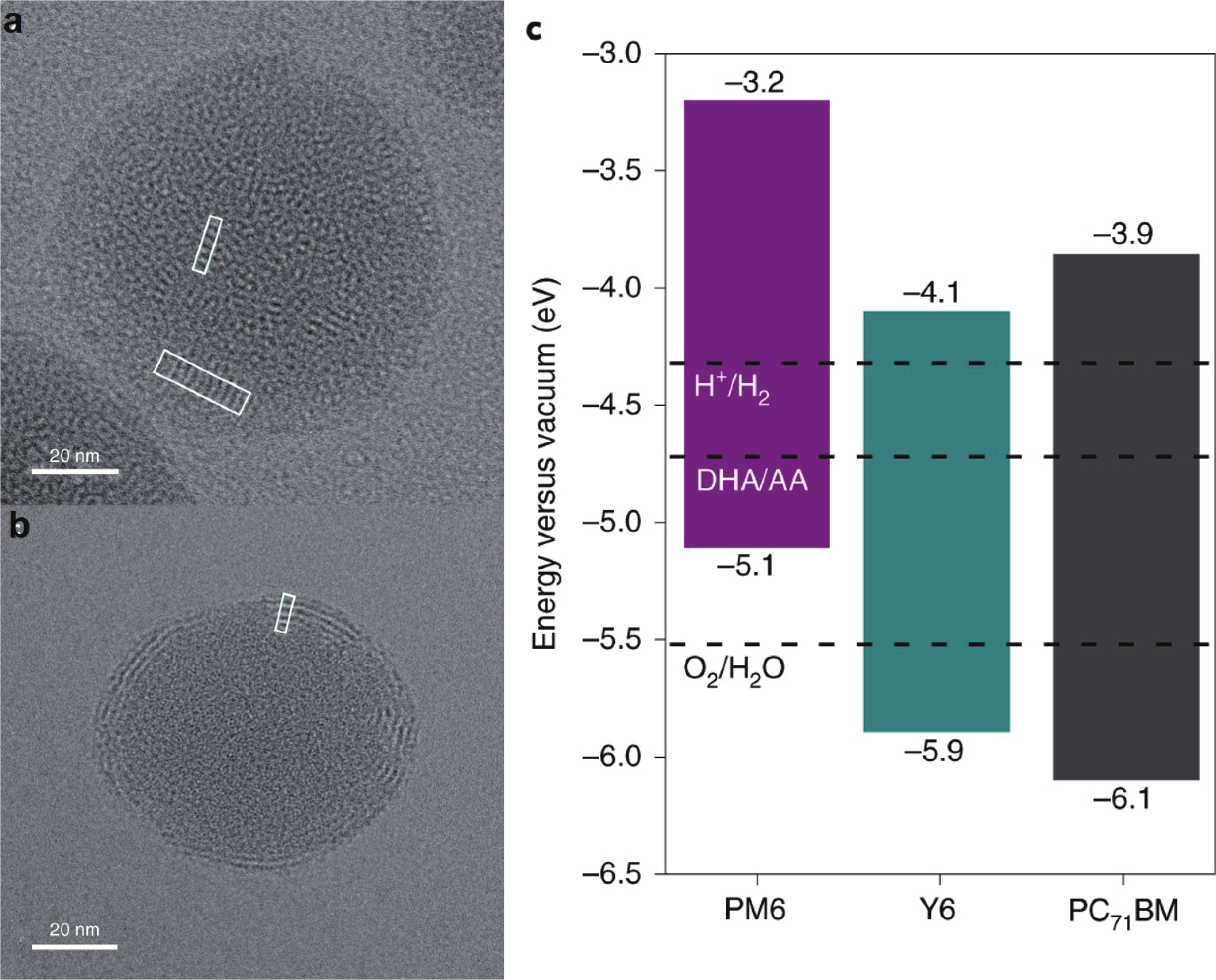
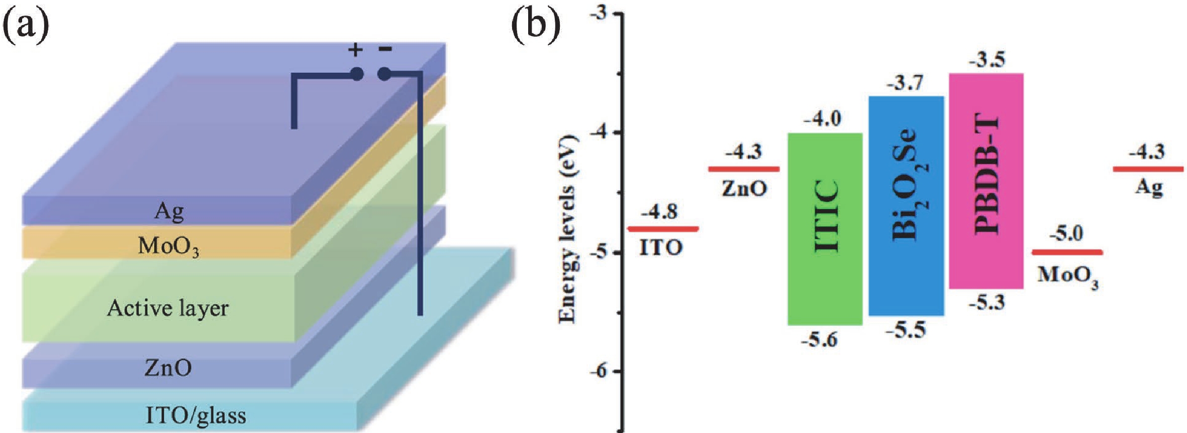
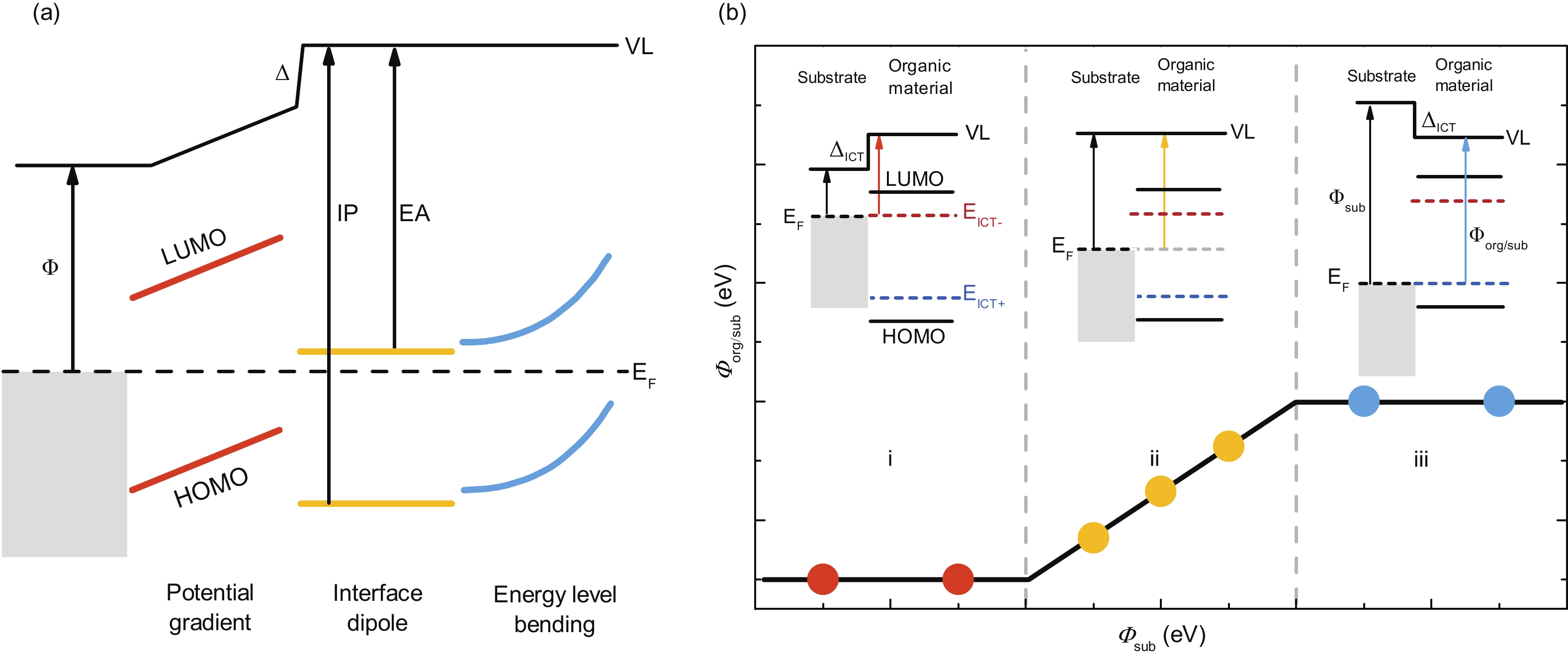
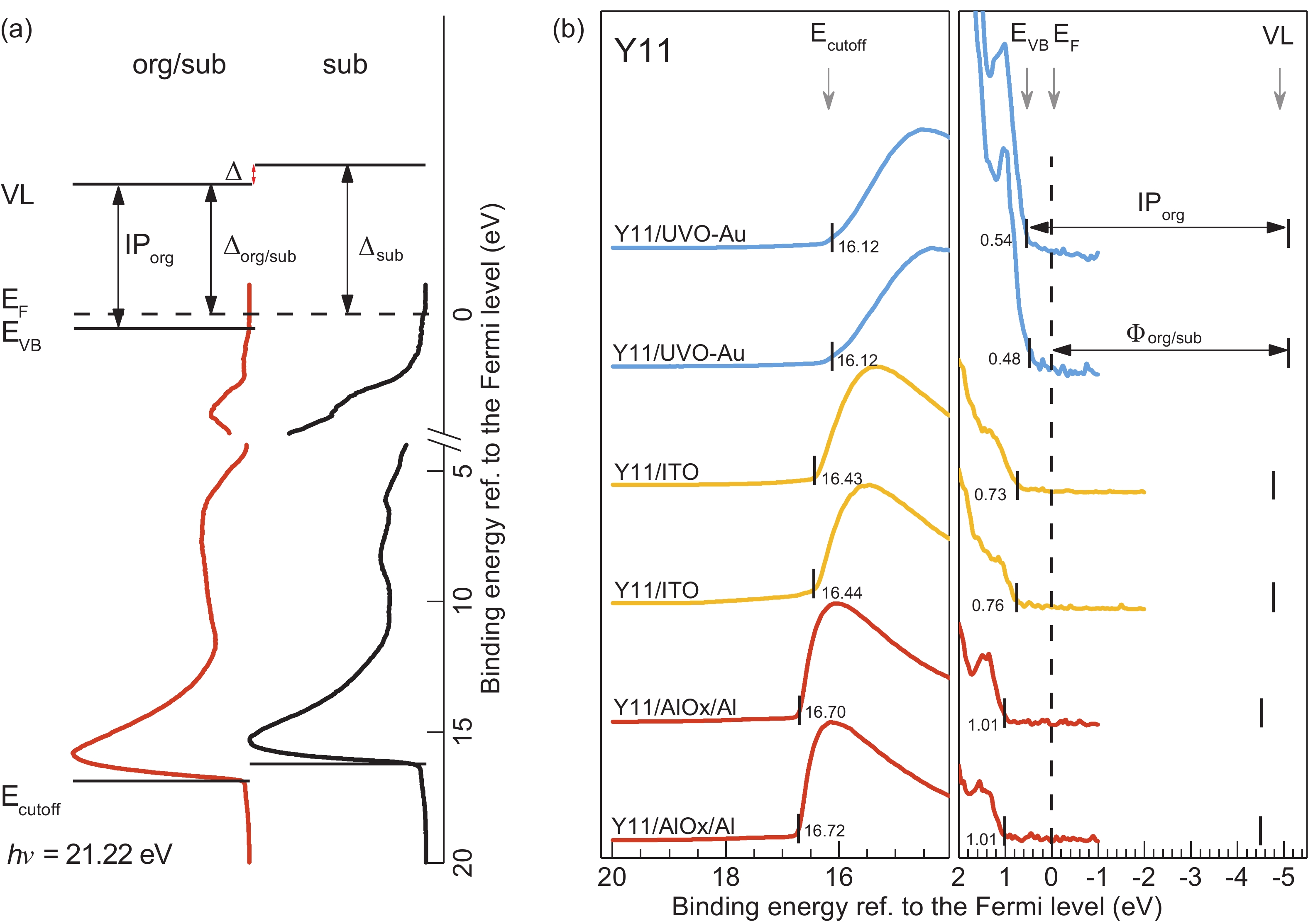
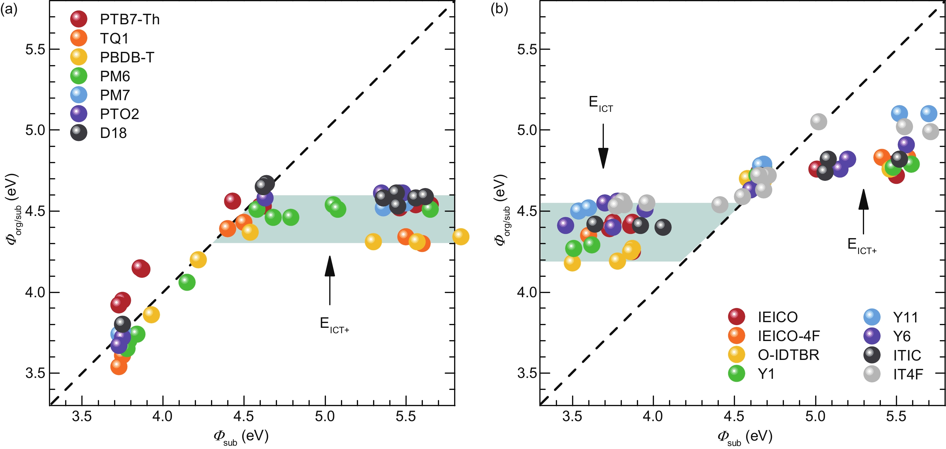
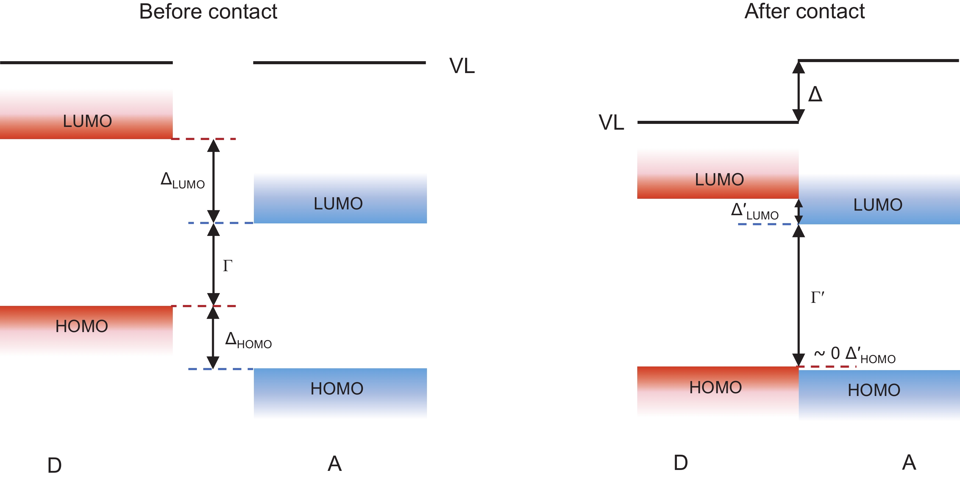
With the emergence of new materials for high-efficiency organic solar cells (OSCs), understanding and finetuning the interface energetics become increasingly important. Precise determination of the so-called pinning energies, one of the critical characteristics of the material to predict the energy level alignment (ELA) at either electrode/organic or organic/organic interfaces, are urgently needed for the new materials. Here, pinning energies of a wide variety of newly developed donors and non-fullerene acceptors (NFAs) are measured through ultraviolet photoelectron spectroscopy. The positive pinning energies of the studied donors and the negative pinning energies of NFAs are in the same energy range of 4.3−4.6 eV, which follows the design rules developed for fullerene-based OSCs. The ELA for metal/organic and inorganic/organic interfaces follows the predicted behavior for all of the materials studied. For organic–organic heterojunctions where both the donor and the NFA feature strong intramolecular charge transfer, the pinning energies often underestimate the experimentally obtained interface vacuum level shift, which has consequences for OSC device performance.
J. Semicond.
2023, 44(3): 032501 doi: 10.1088/1674-4926/44/3/032501
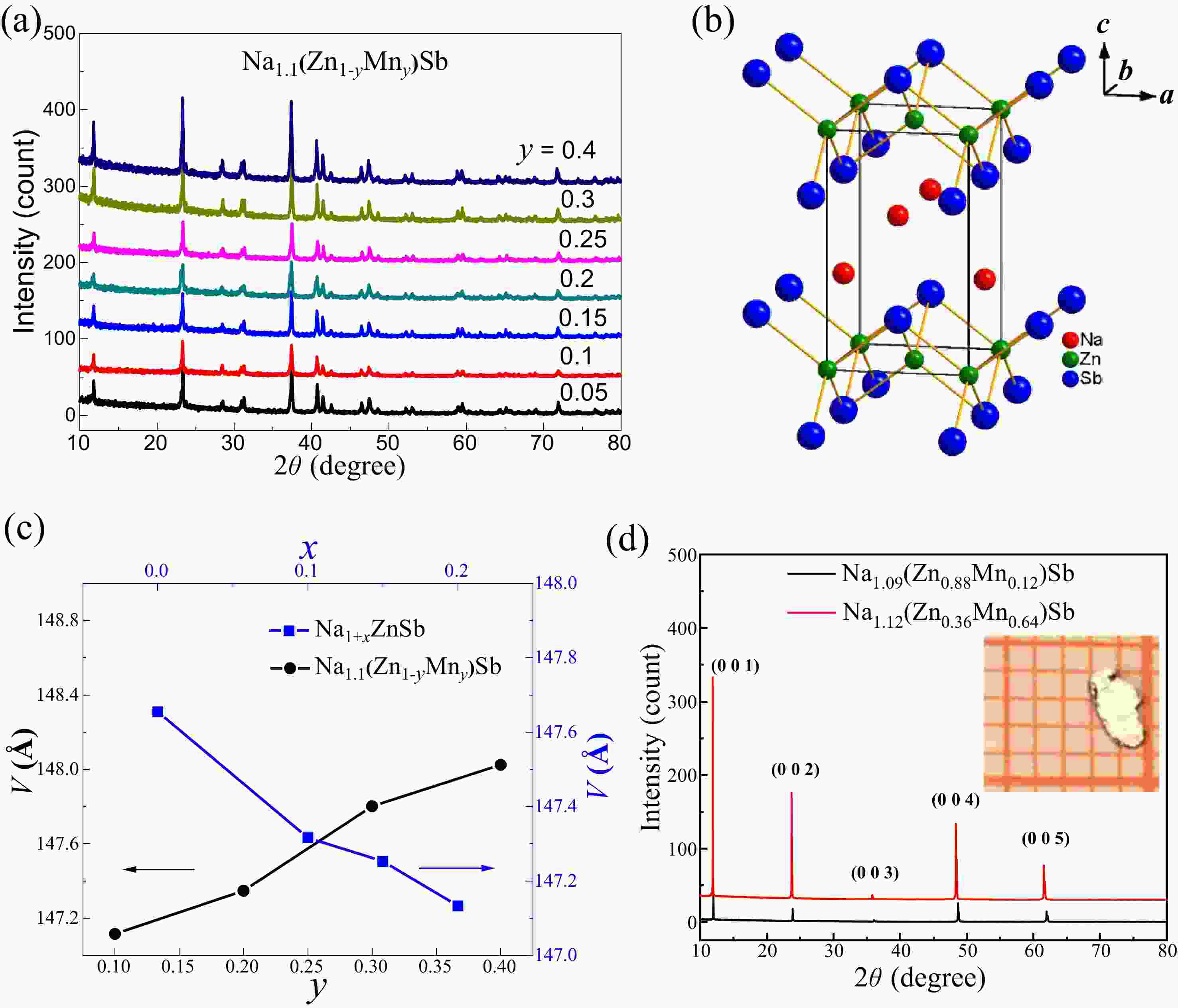
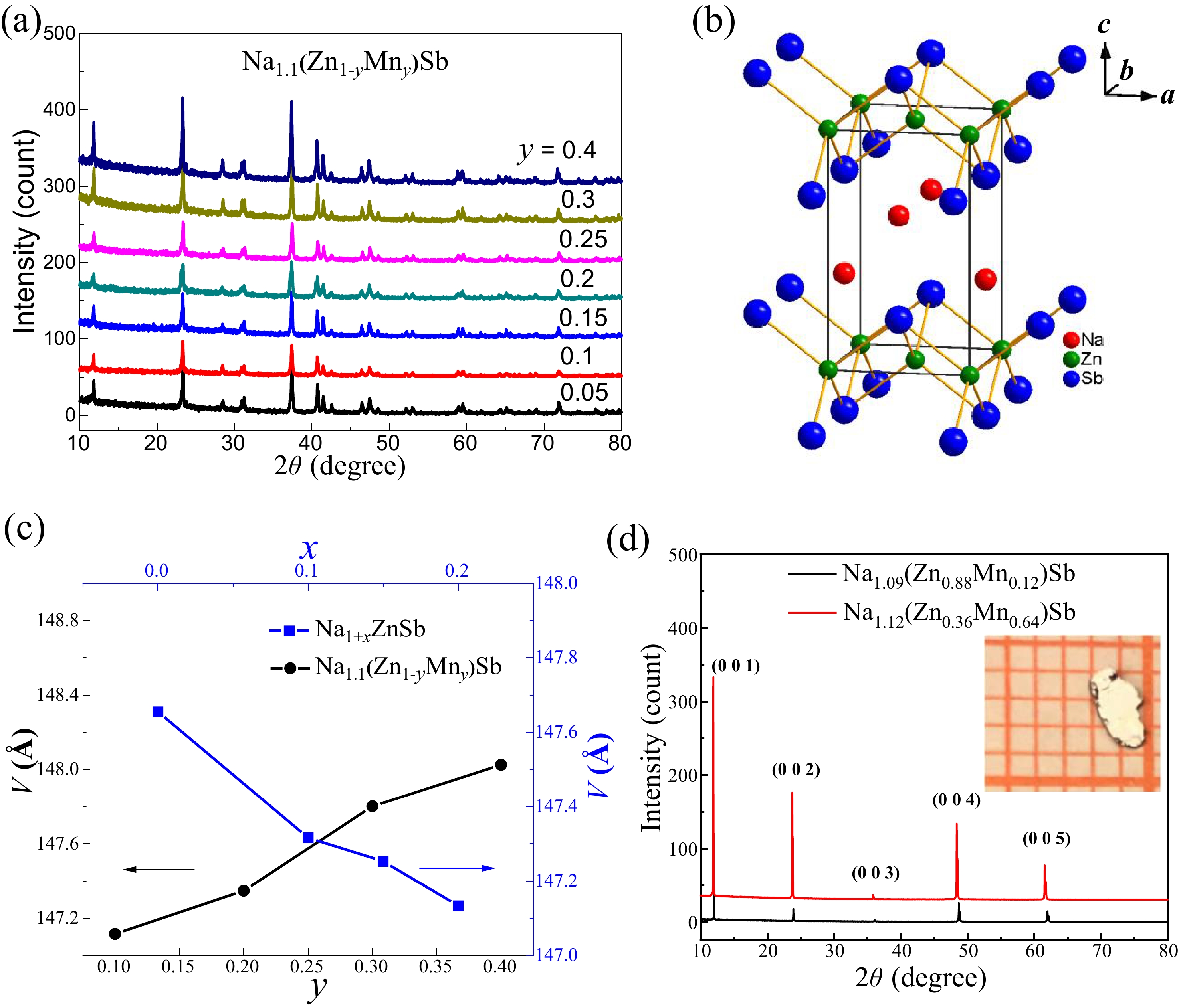
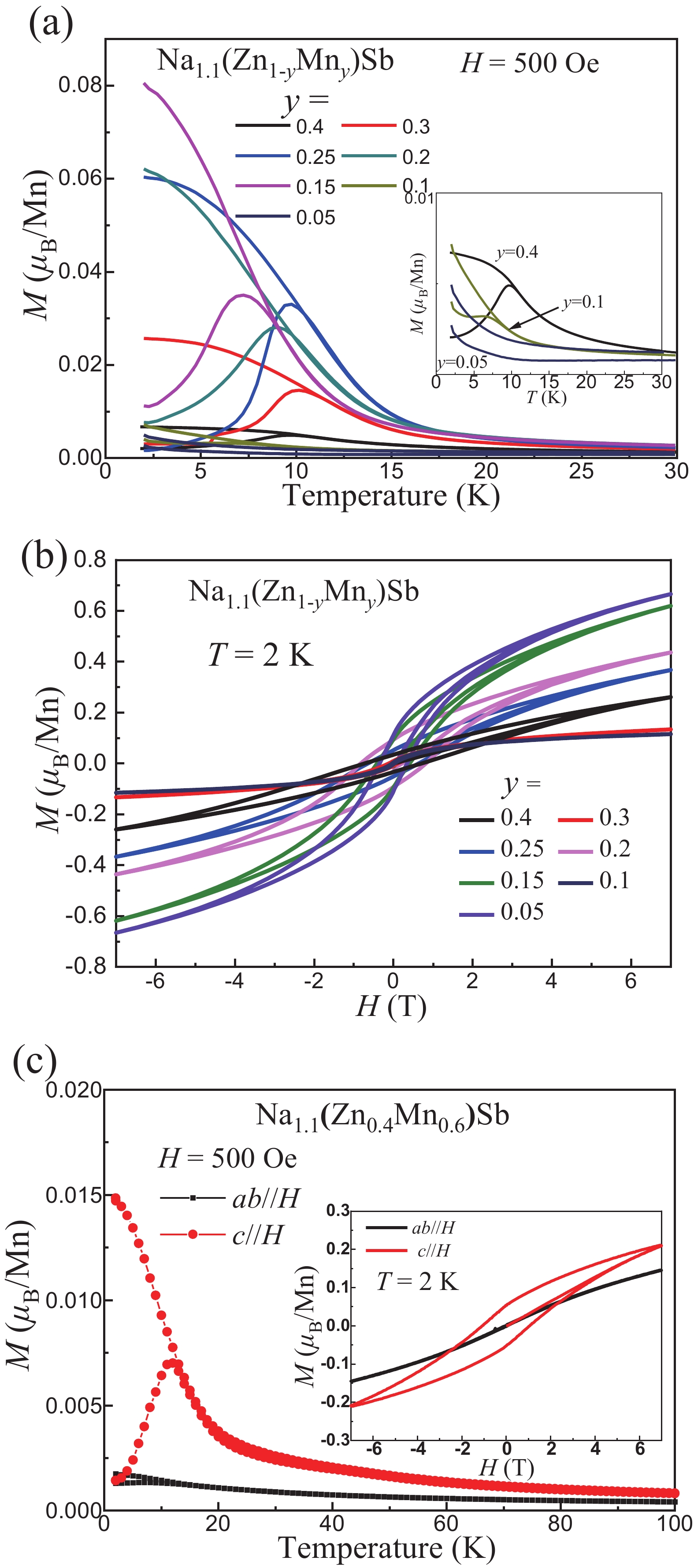
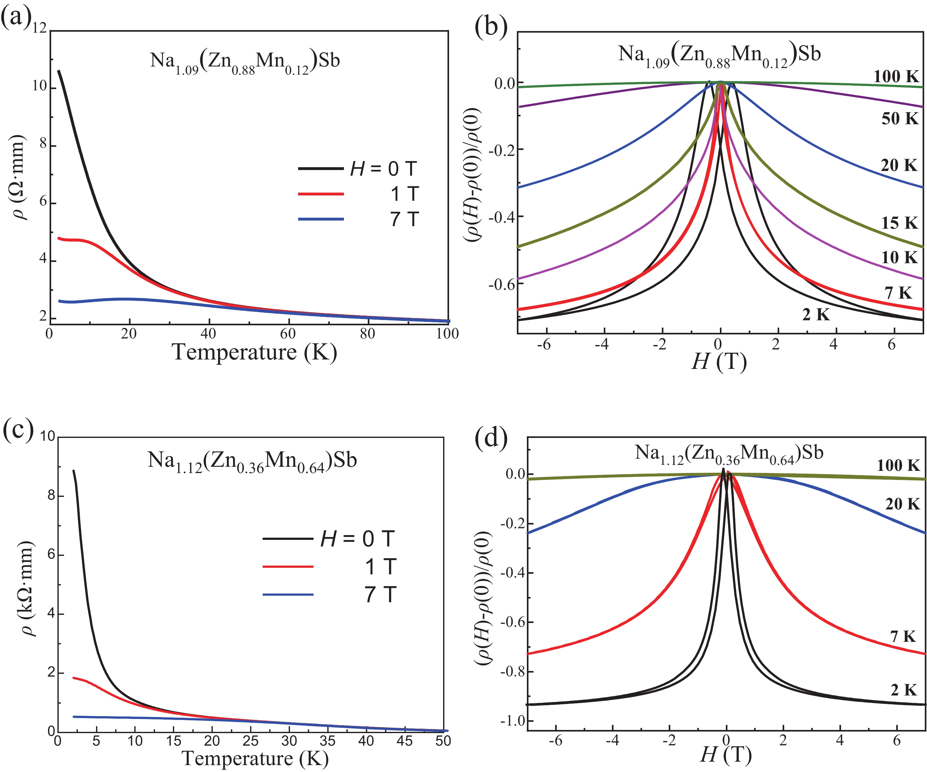
We report the study of magnetic and transport properties of polycrystalline and single crystal Na(Zn,Mn)Sb, a new member of “111” type of diluted magnetic materials. The material crystallizes into Cu2Sb-type structure which is isostructural to “111” type Fe-based superconductors. With suitable carrier and spin doping, the Na(Zn,Mn)Sb establishes spin-glass ordering with freezing temperature (Tf) below 15 K. Despite lack of long-range ferromagnetic ordering, Na(Zn,Mn)Sb single crystal still shows sizeable anomalous Hall effect below Tf. Carrier concentration determined by Hall effect measurements is over 1019 cm–3. More significantly, we observe colossal negative magnetoresistance (MR ≡ [ρ(H) − ρ(0)]/ρ(0)) of –94% in the single crystal sample.


J. Semicond.
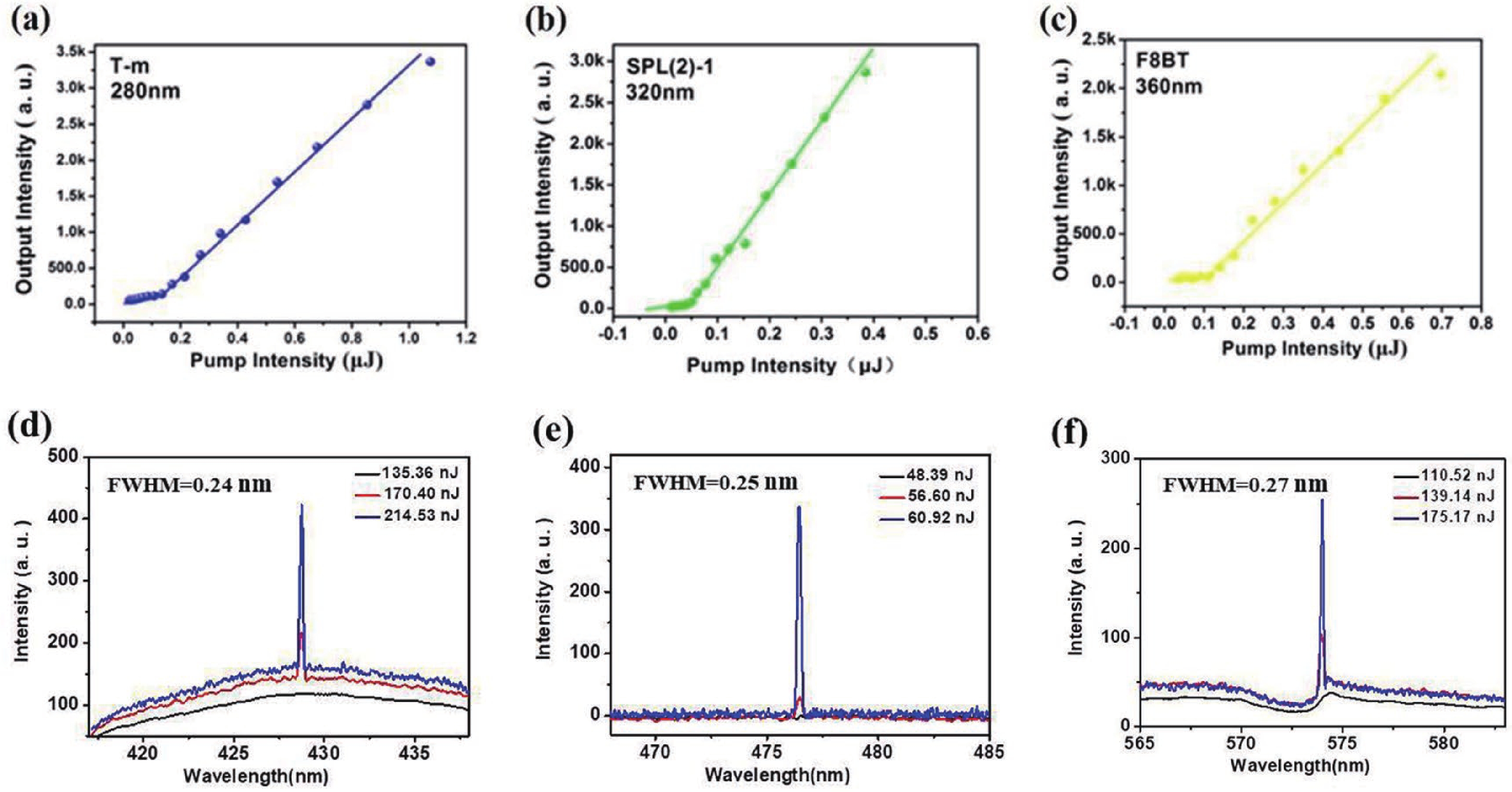
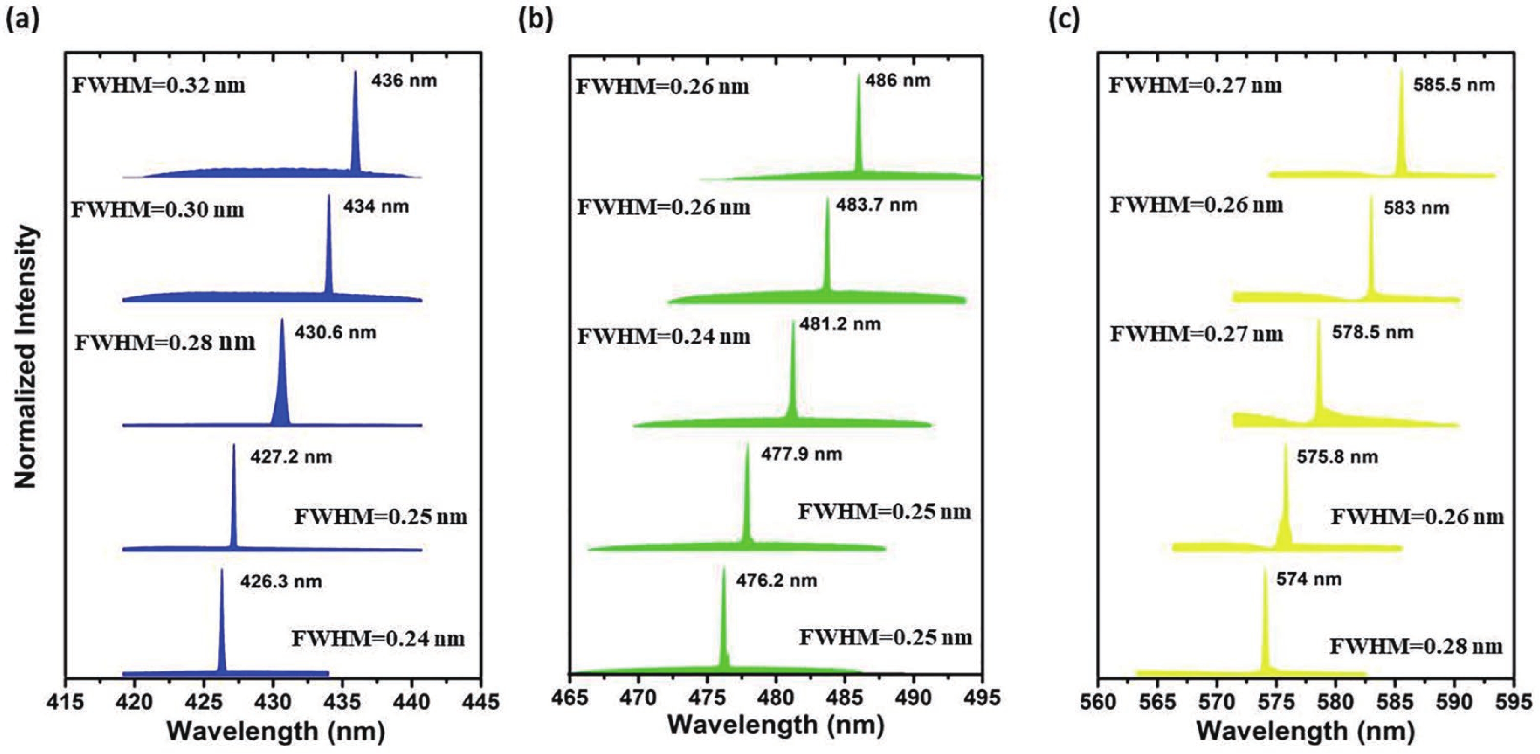
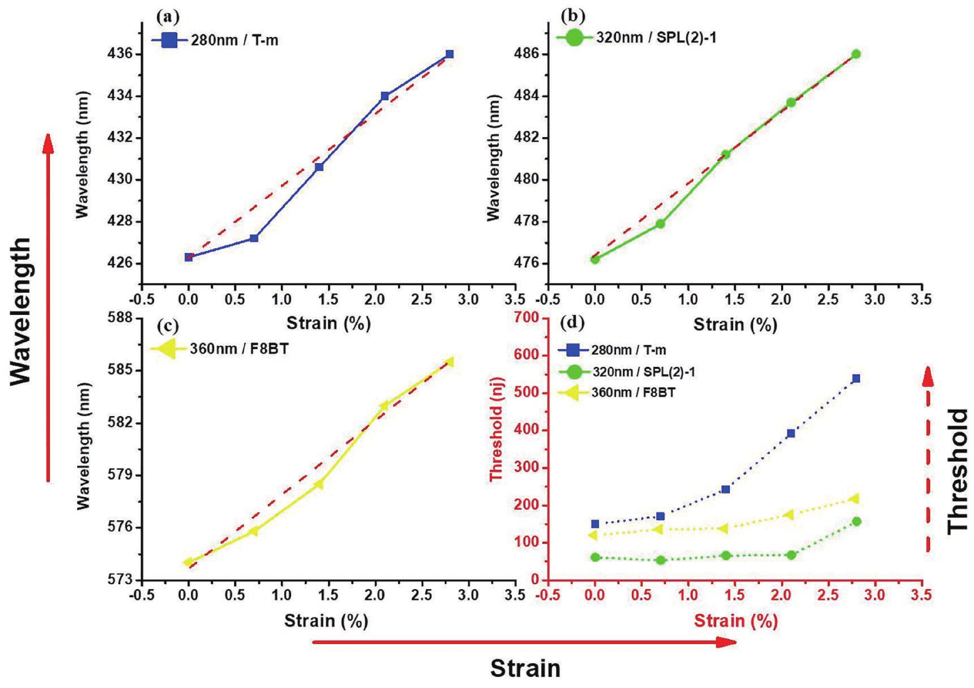
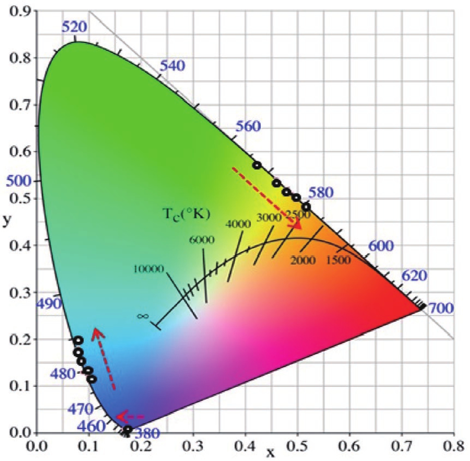
2023, 44(3): 032601 doi: 10.1088/1674-4926/44/3/032601
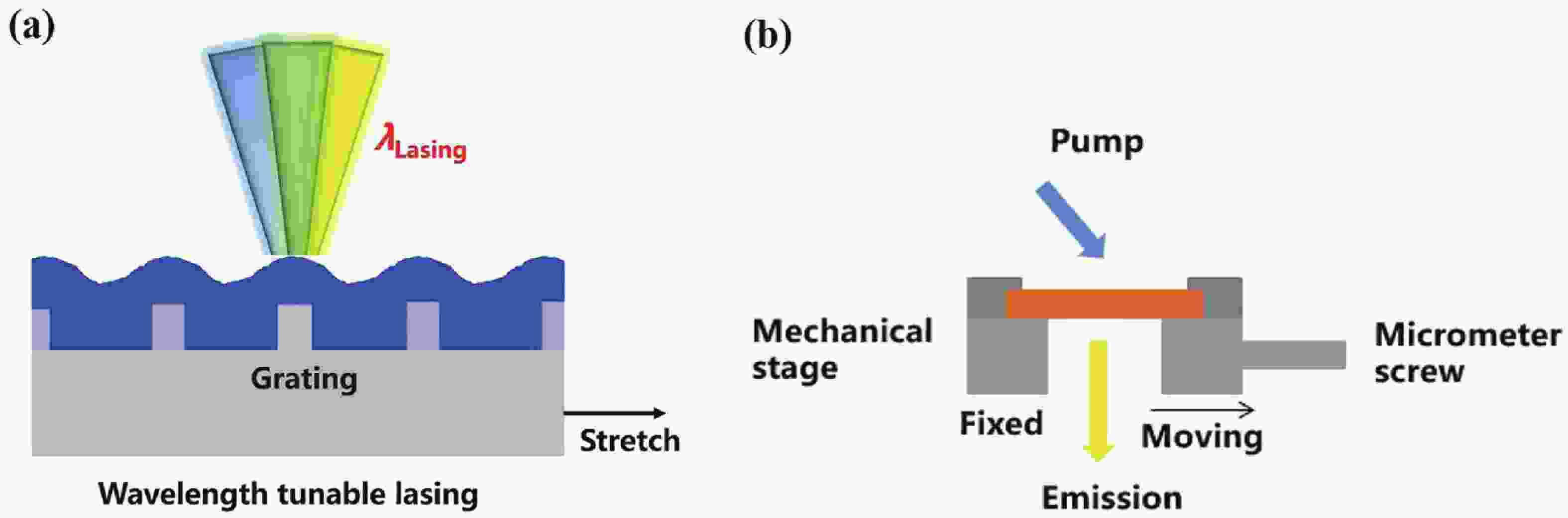
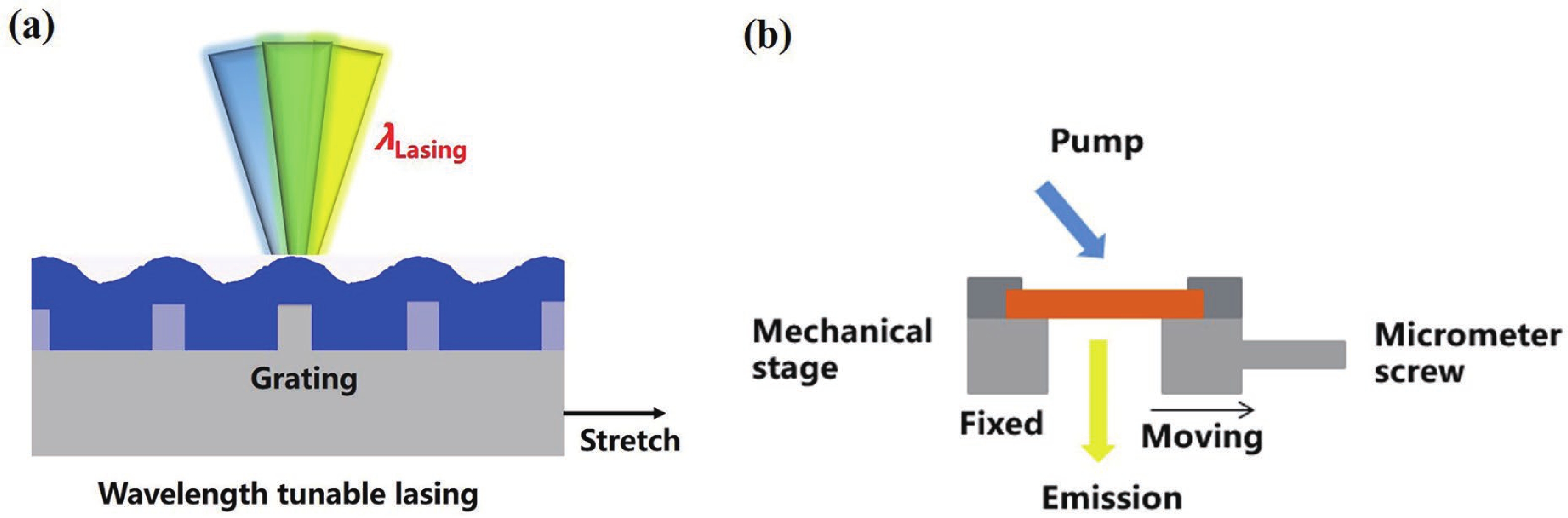
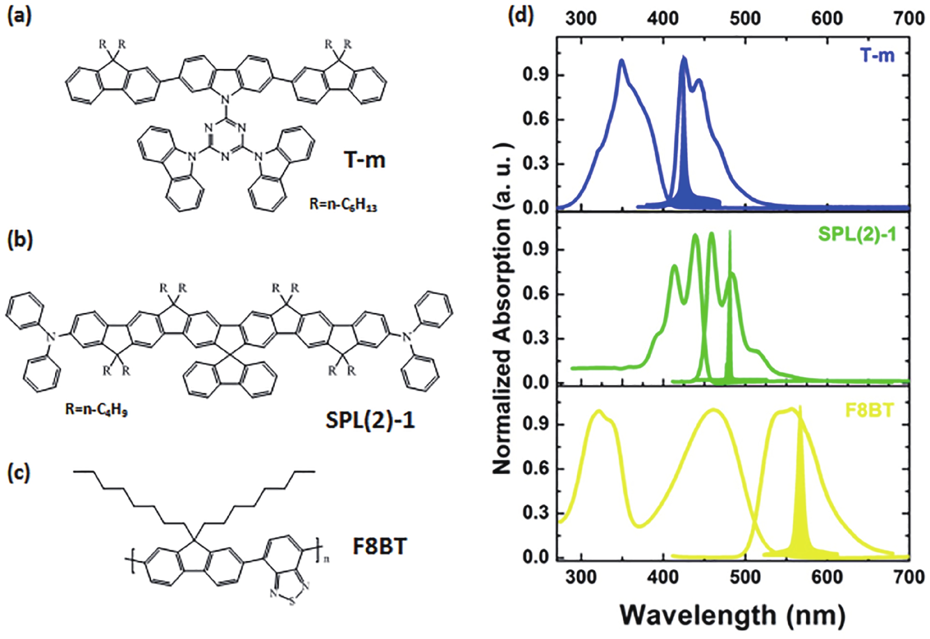
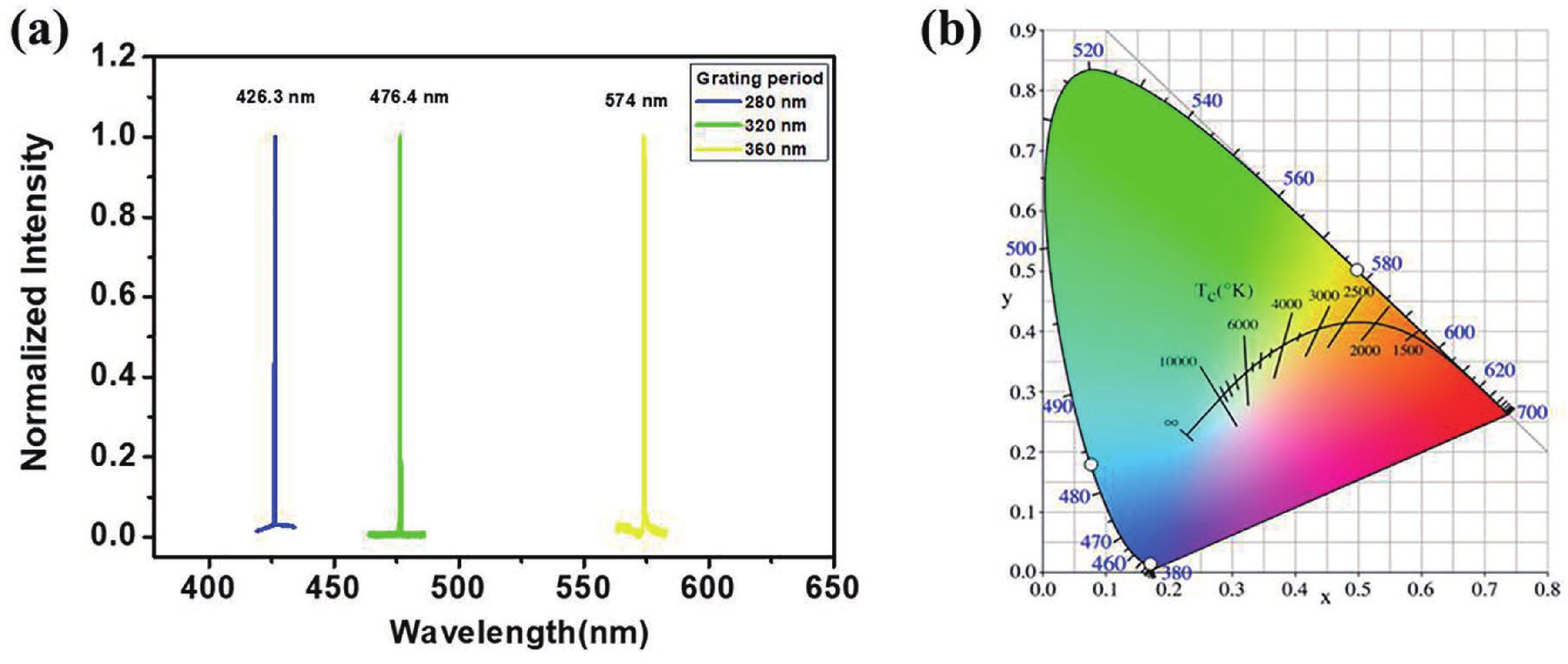
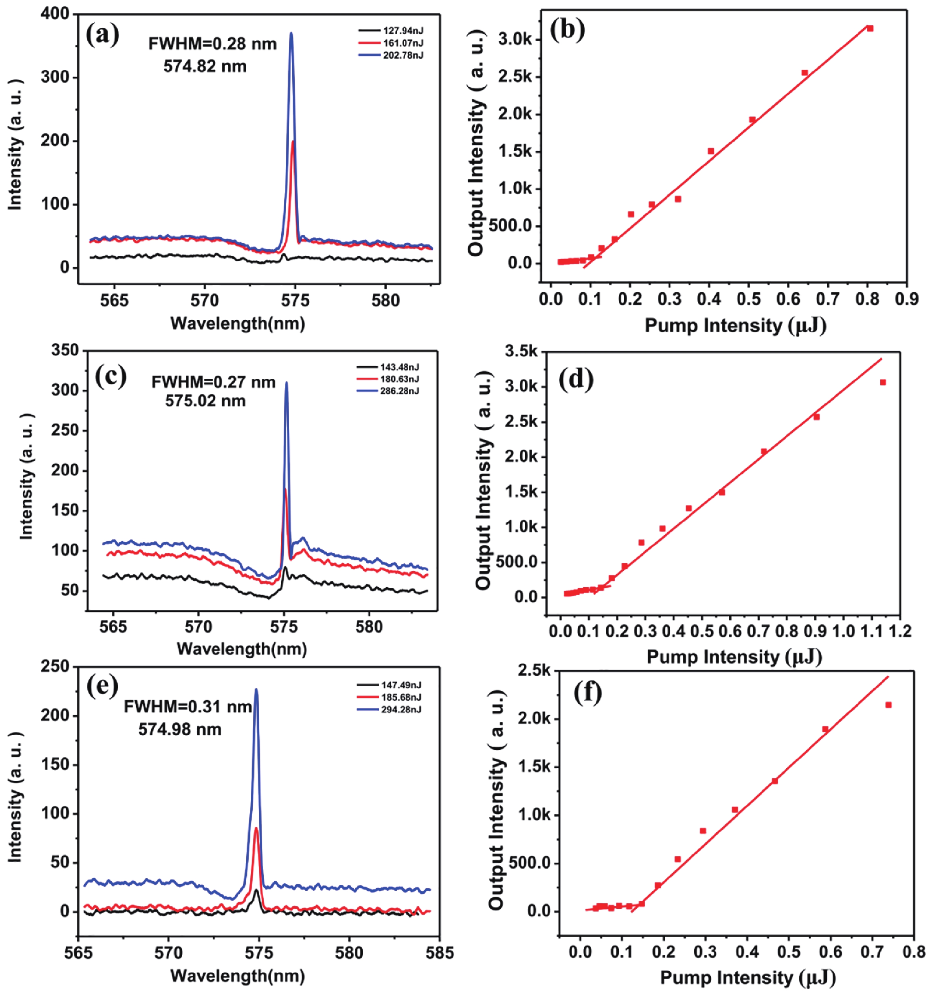
Wavelength-tunable organic semiconductor lasers based on mechanically stretchable polydimethylsiloxane (PDMS) gratings were developed. The intrinsic stretchability of PDMS was explored to modulate the period of the distributed feedback gratings for fine tuning the lasing wavelength. Notably, elastic lasers based on three typical light-emitting molecules show comparable lasing threshold values analogous to rigid devices and a continuous wavelength tunability of about 10 nm by mechanical stretching. In addition, the stretchability provides a simple solution for dynamically tuning the lasing wavelength in a spectral range that is challenging to achieve for inorganic counterparts. Our work has provided a simple and efficient method of fabricating tunable organic lasers that depend on stretchable distributed feedback gratings, demonstrating a significant step in the advancement of flexible organic optoelectronic devices.

J. Semicond.
2023, 44(3): 032602 doi: 10.1088/1674-4926/44/3/032602
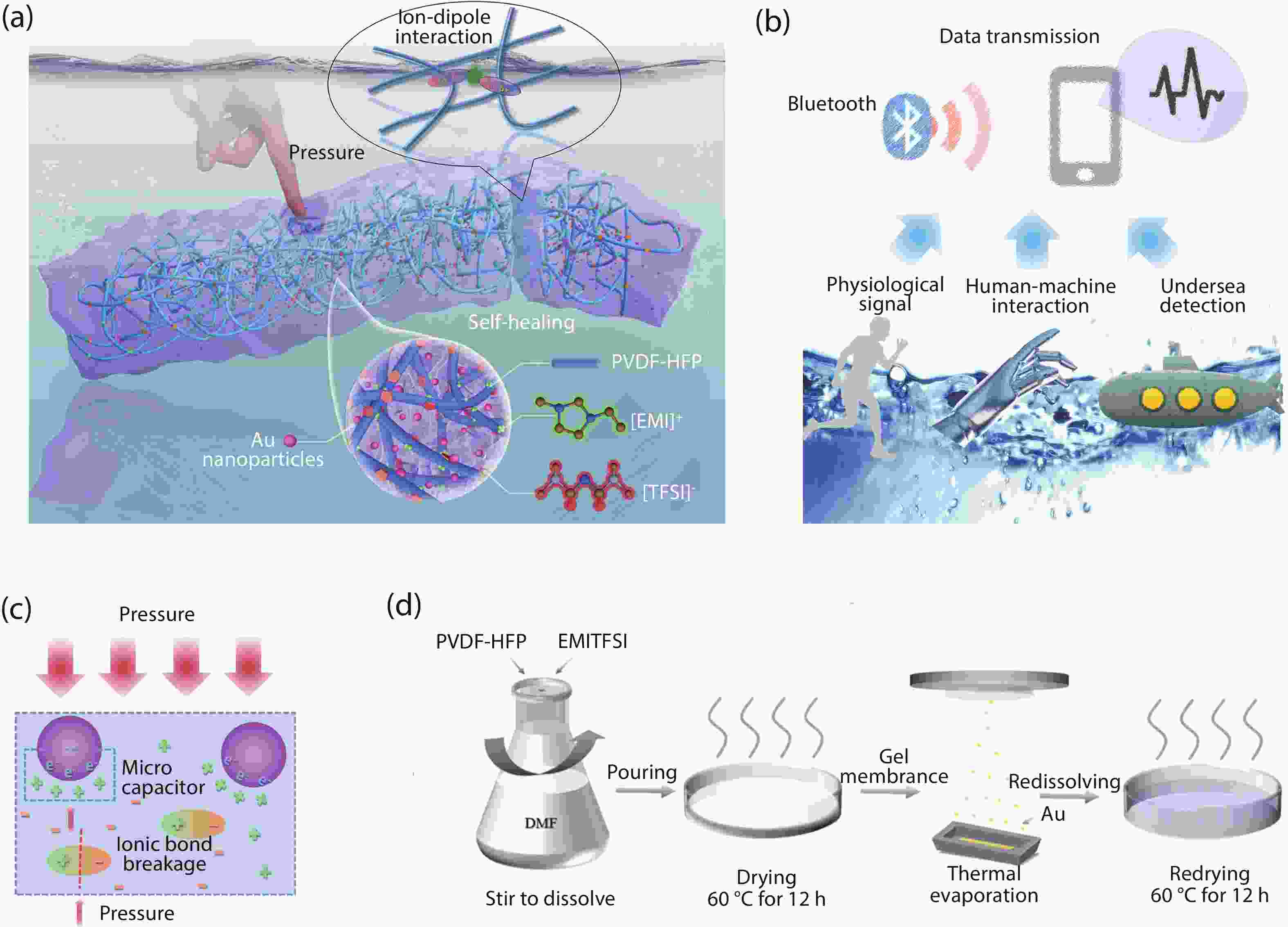
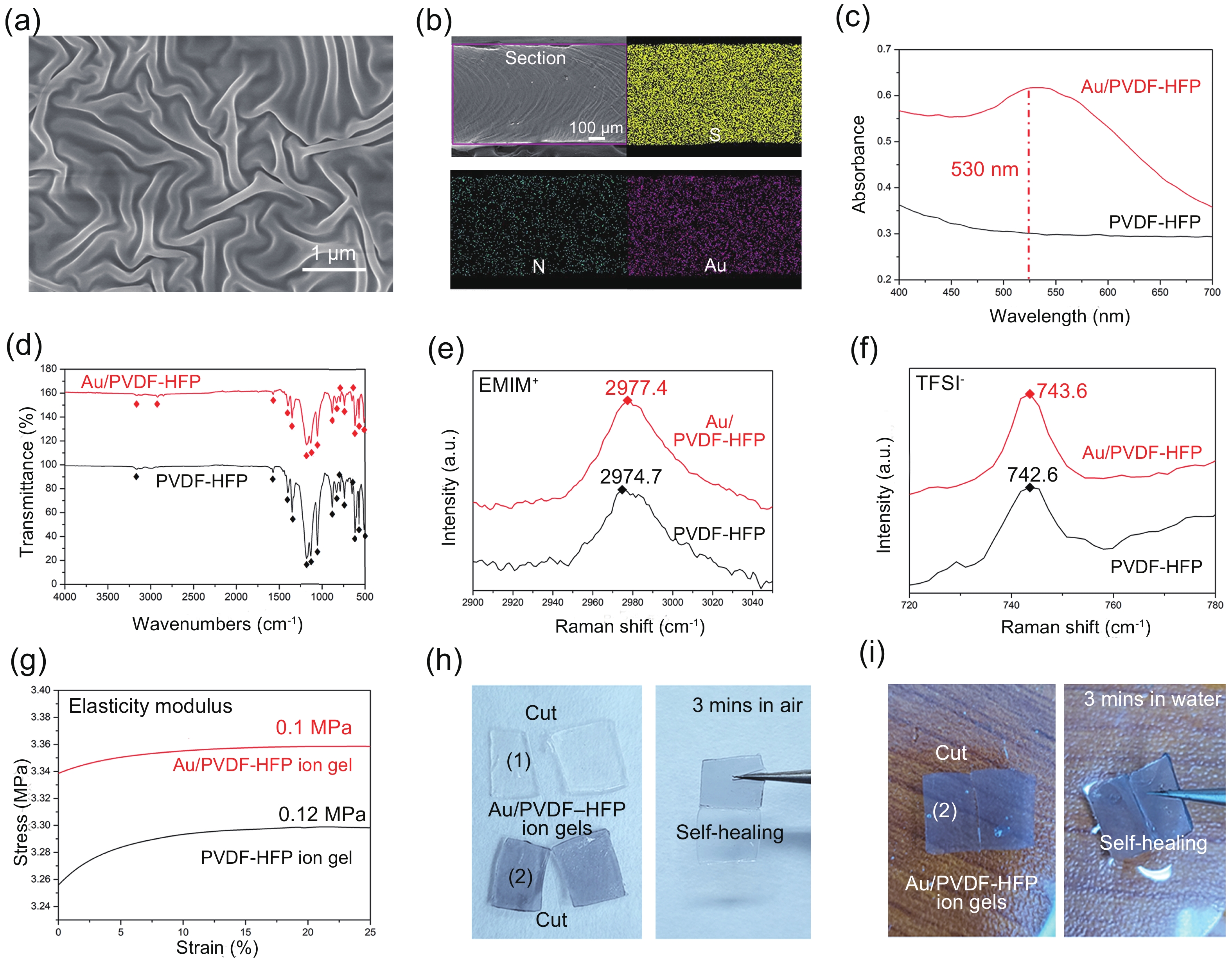
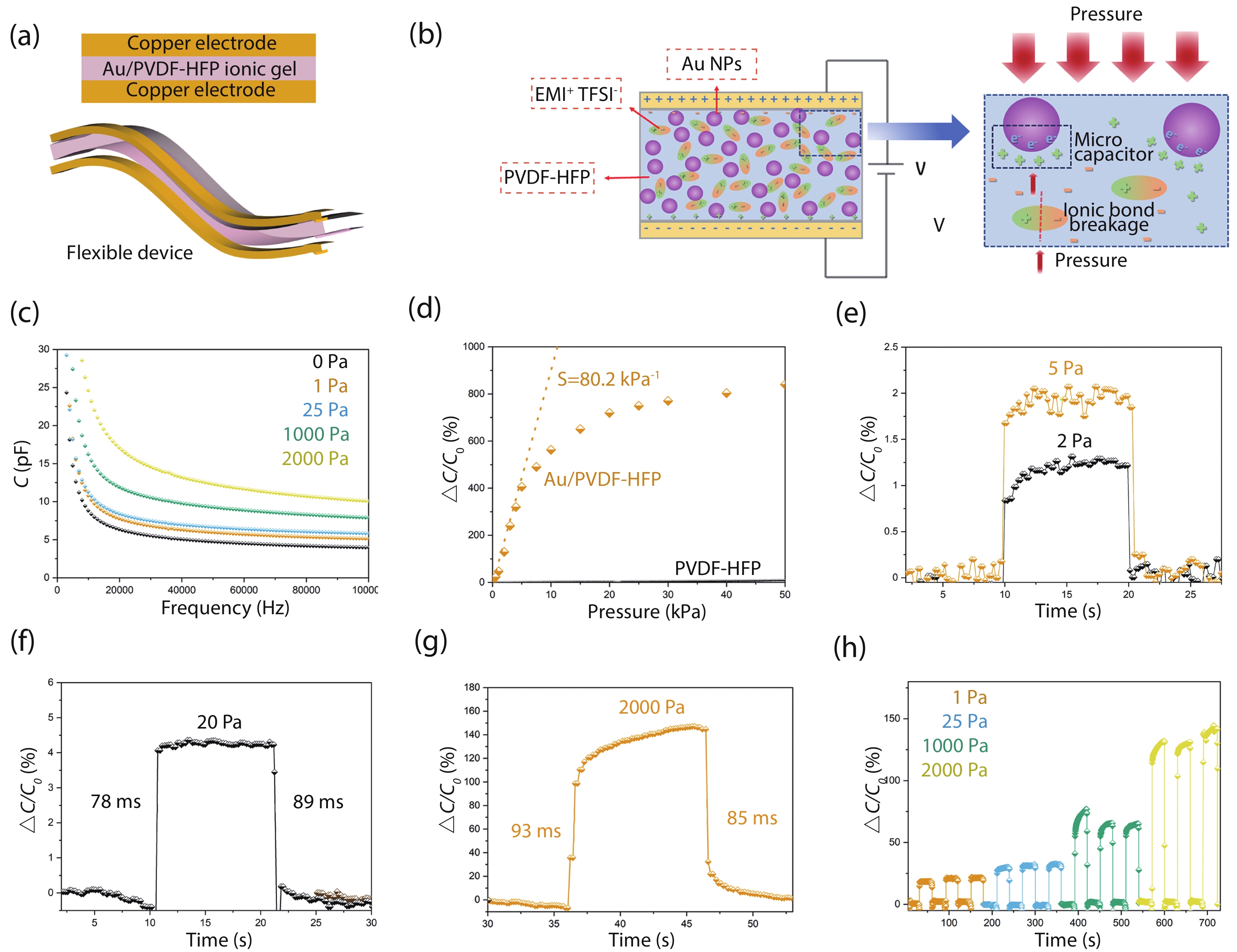
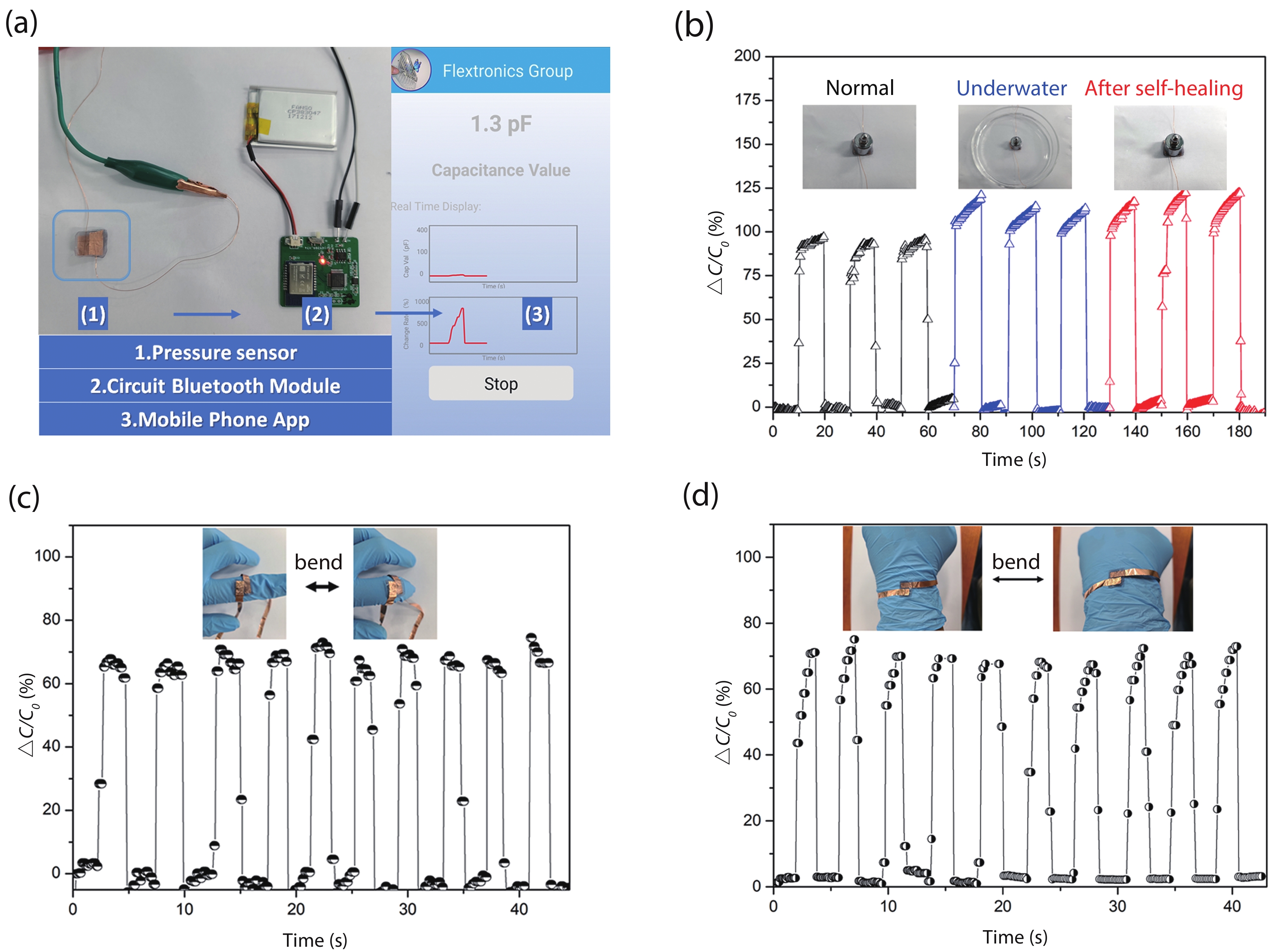
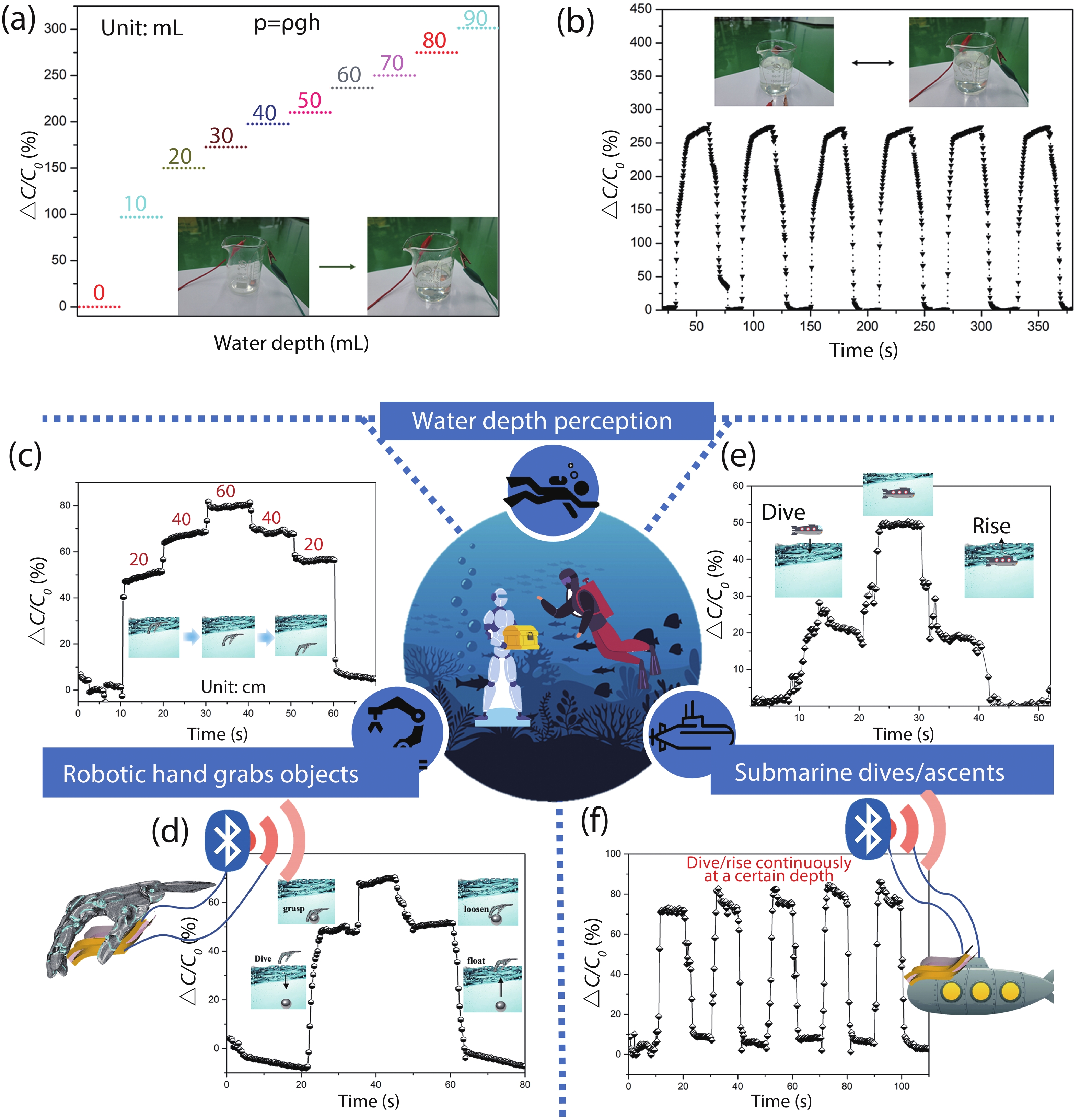
Ionic gels can be potentially used in wearable devices owing to their high humidity resistance and non-volatility. However, the applicability of existing ionic gel pressure sensors is limited by their low sensitivity. Therefore, it is very important to develop an ionic gel pressure sensor with high sensitivity and a wide pressure detection range without sacrificing mechanical stretchability and self-healing ability. Herein, we report an effective strategy for developing pressure sensors based on ionic gel composites consisting of high-molecular-weight polymers, ionic liquids, and Au nanoparticles. The resulting capacitive pressure sensors exhibit high pressure sensitivity, fast response, and excellent self-healing properties. The sensors composed of highly hydrophobic polymers and ionic liquids can be used to track underwater movements, demonstrating broad application prospects in human motion state monitoring and underwater mechanical operations.
J. Semicond.
2023, 44(3): 032701 doi: 10.1088/1674-4926/44/3/032701
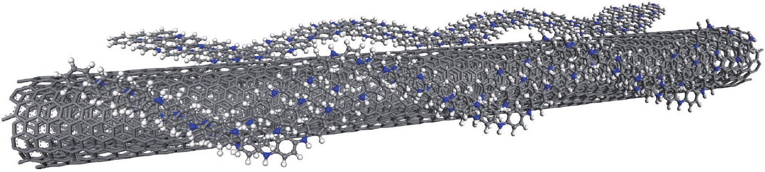
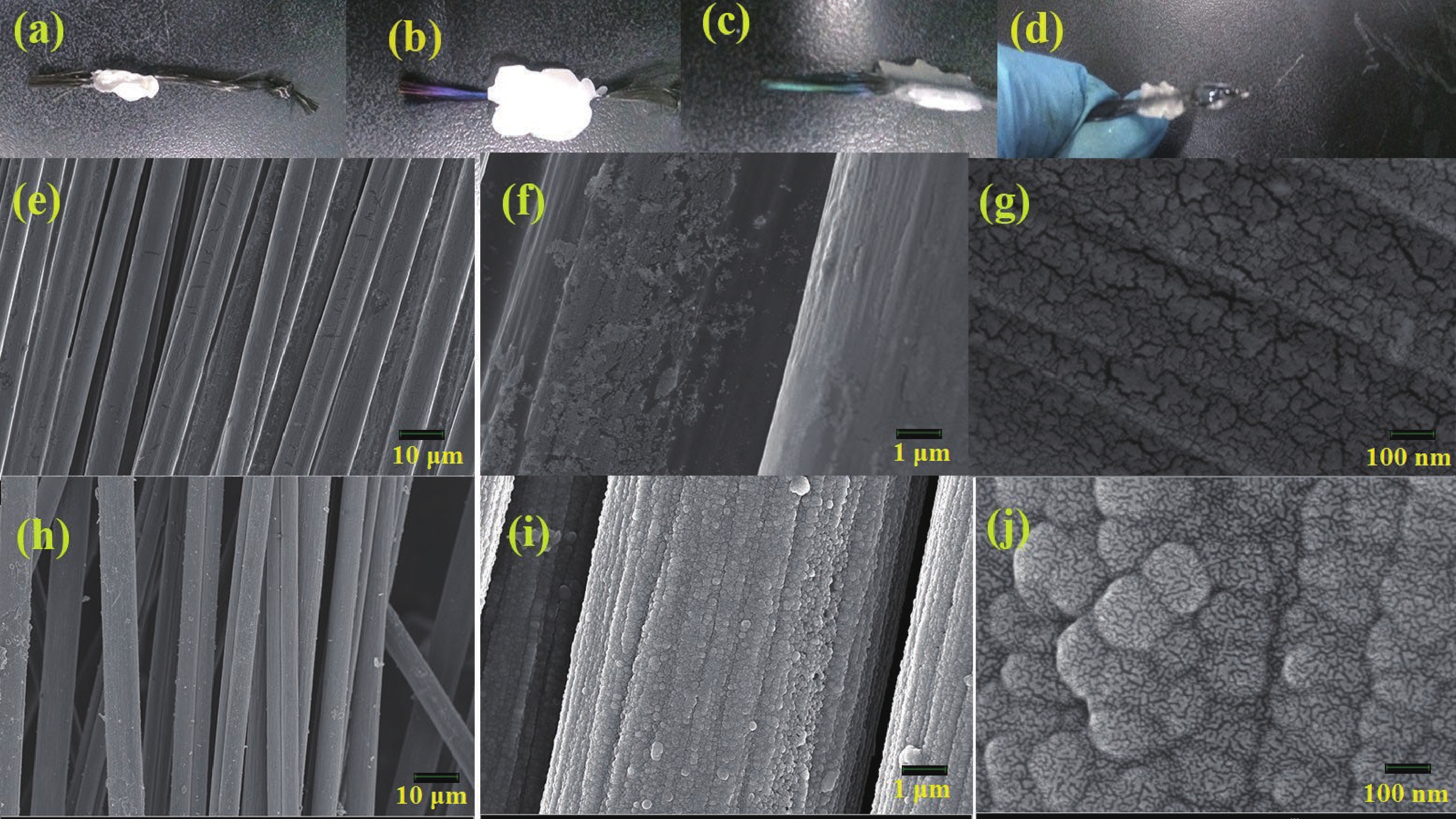
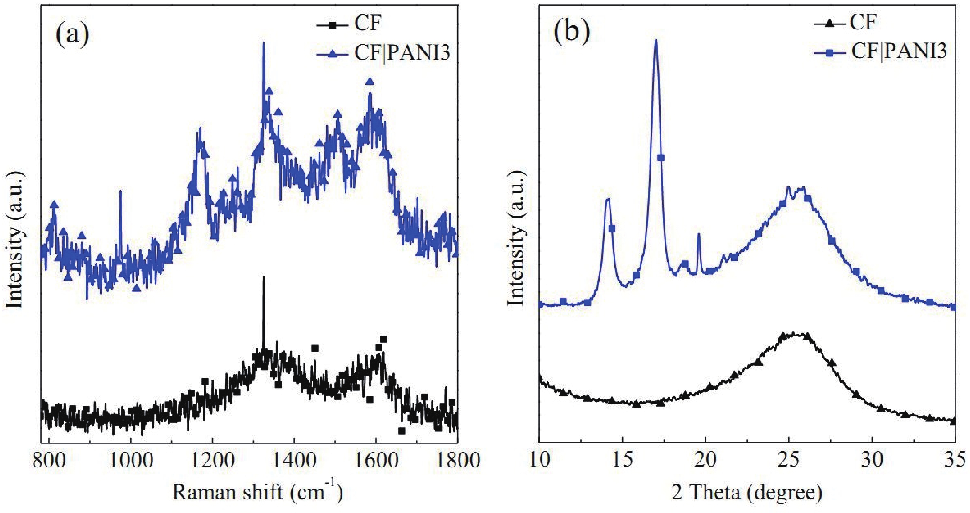
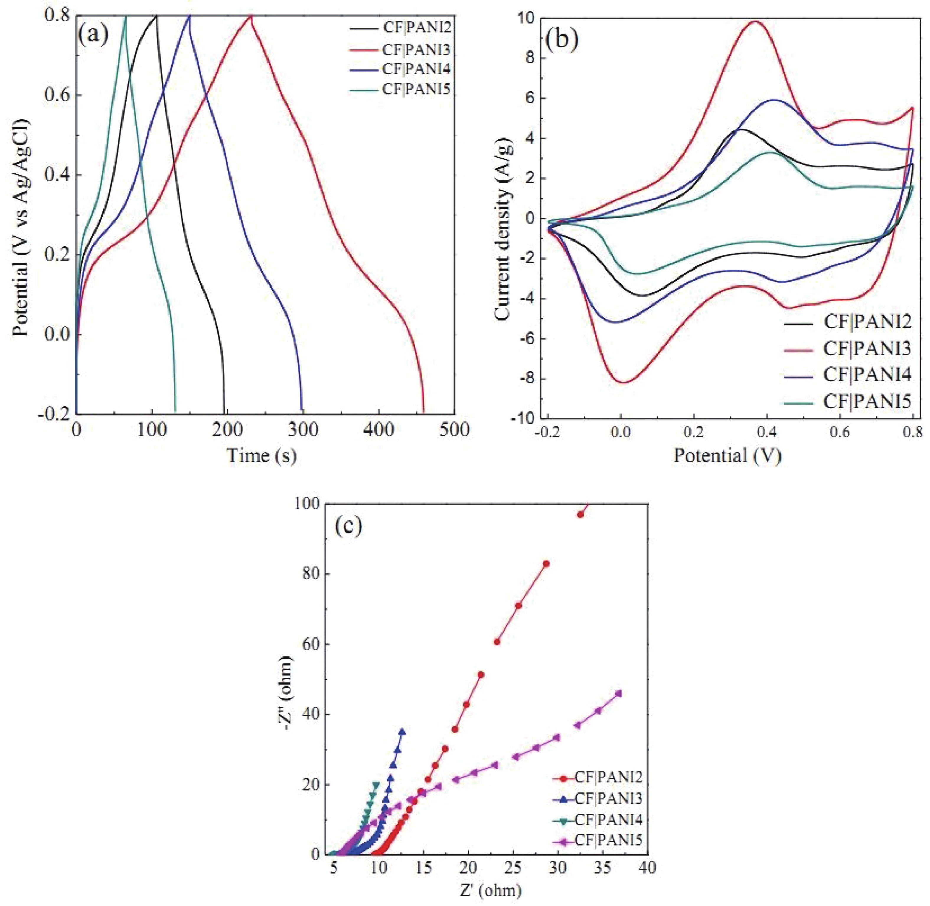
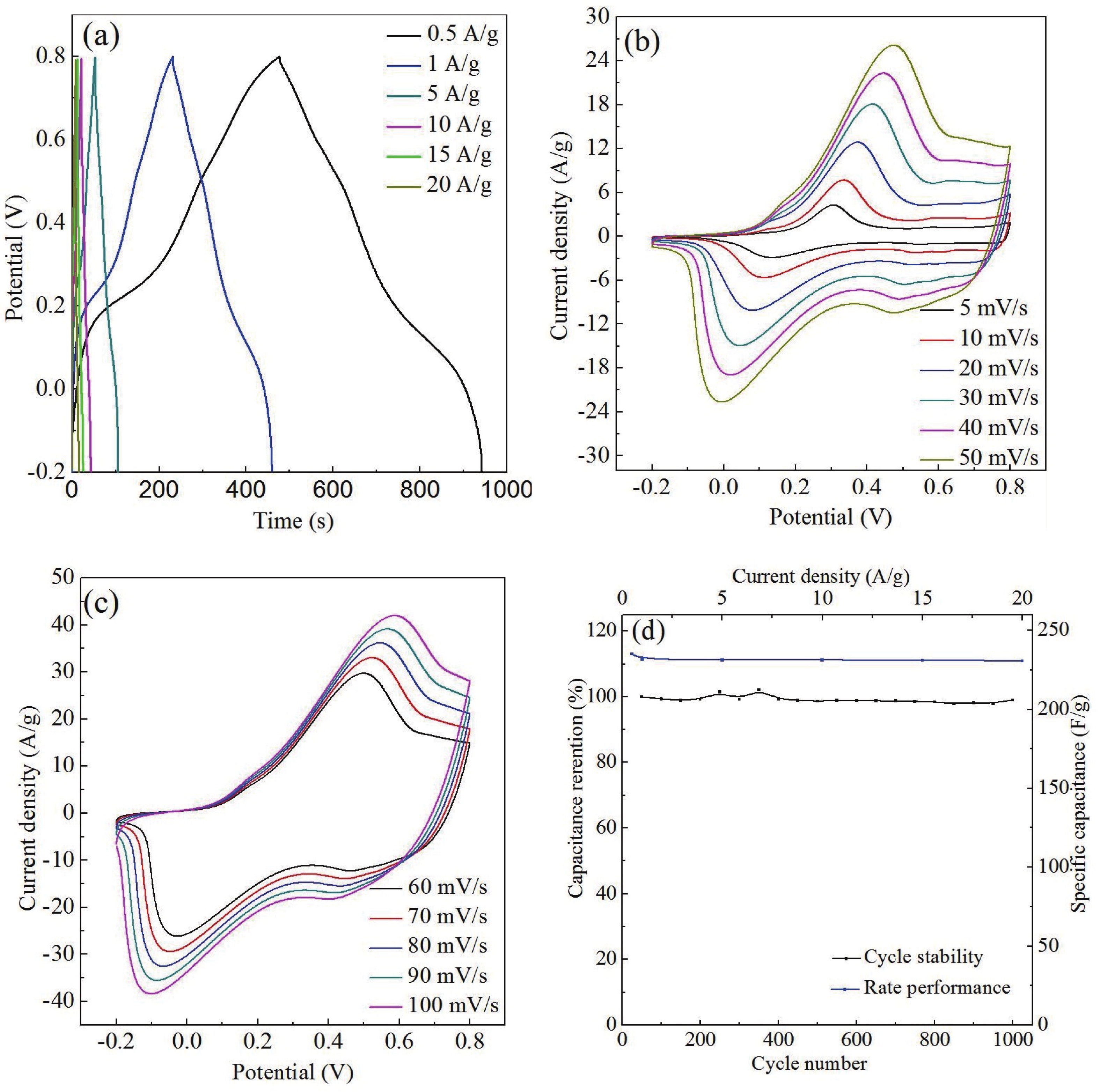
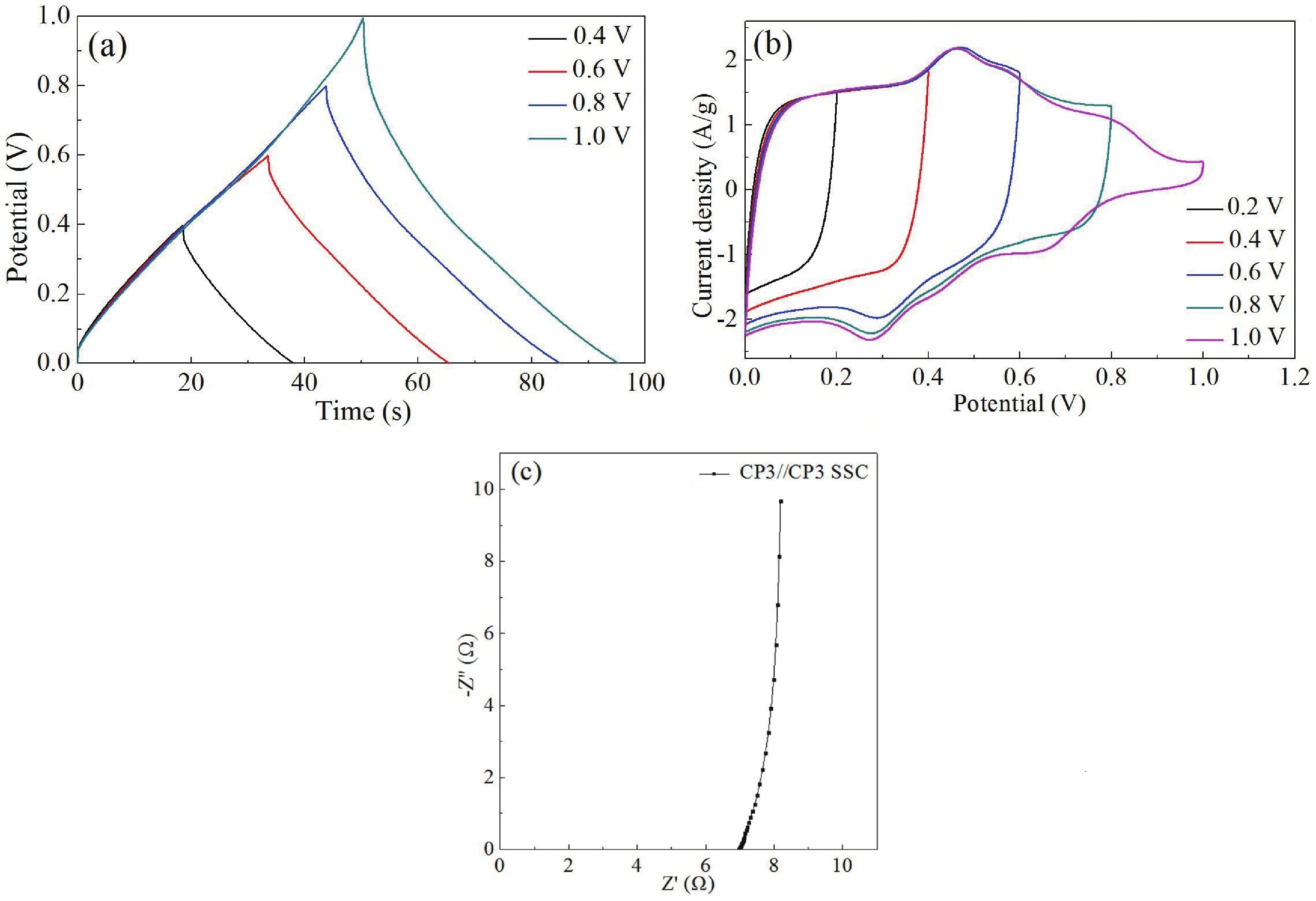
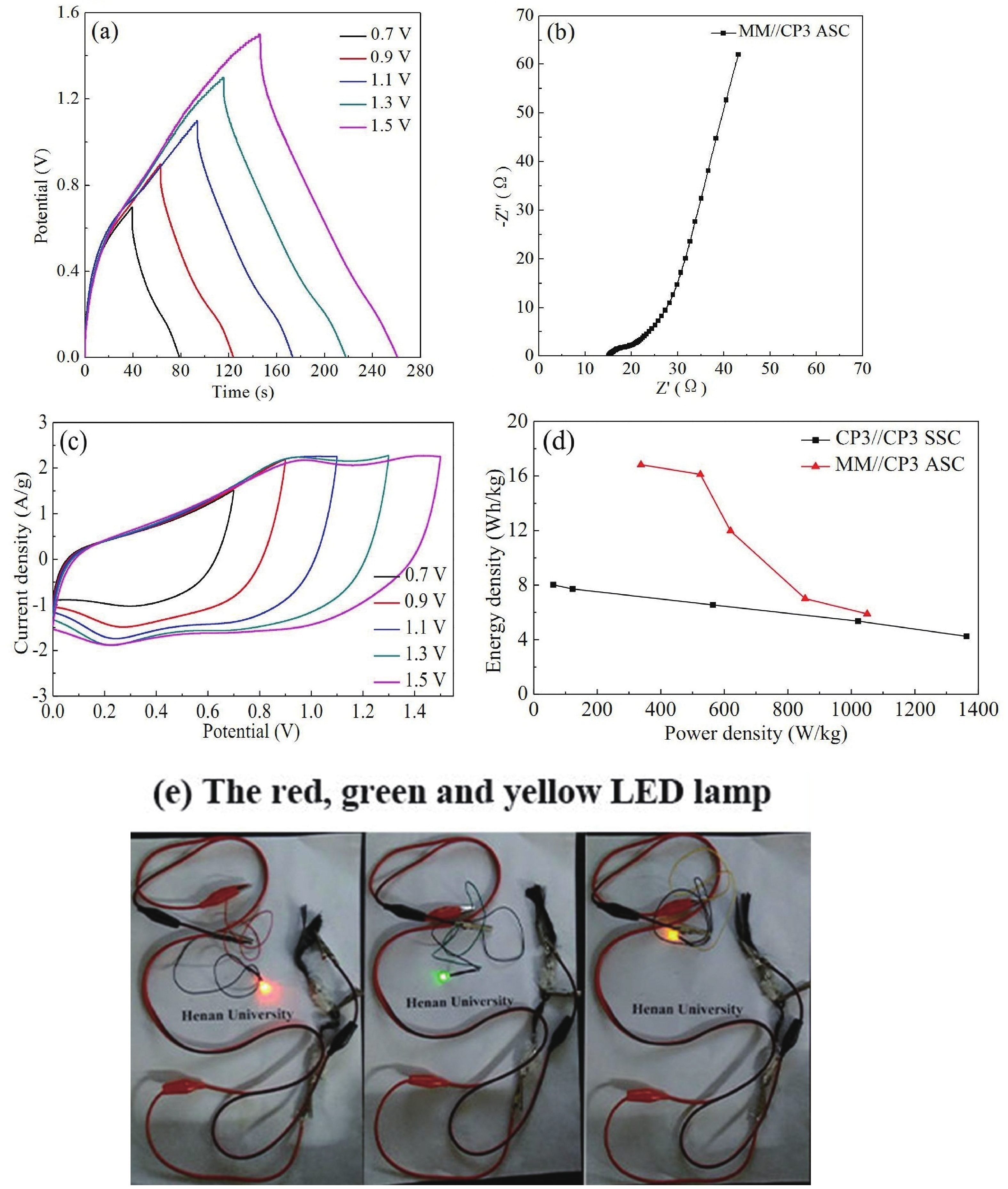
In this work, carbon fiber and polyaniline (CF|PANI) composites are prepared by using an electrochemical polymerization method. The morphology and composition characterization results show that the PANI nanospheres are successfully synthesized and uniformly coated on the CF. When the electrodeposition period is 300 cycles, the as-prepared CF|PANI electrode exhibits good specific capacitance of 231.63 F/g at 1 A/g, high performance of 98.14% retention rate from 0.5 to 20 A/g, and excellent cycle stability with only 0.96% capacity loss after 1000 cycles. This is ascribed to the internal resistance that was significantly reduced without binders, which helps to the CF|PANI electrode maintains high operating potential and pseudo-capacitance performance at high current density. The symmetrical supercapacitor based on two CF|PANI electrodes connecting by acidic PVA-H2SO4 gel electrolyte exhibits an energy density of 6.55 W·h/kg at a power density of 564.37 W/kg. In addition, the asymmetric supercapacitor based on MoS2|MWCNTs and CF|PANI electrodes with neutral PVA-Na2SO4 gel electrolyte shows an energy density of 16.12 W·h/kg at a power density of 525.03 W/kg. These results indicate that the low internal resistance contributes to the high energy density of symmetrical supercapacitors and asymmetric supercapacitors at high current density and high power density, which is significant for its practical application.
J. Semicond.
2023, 44(3): 032702 doi: 10.1088/1674-4926/44/3/032702
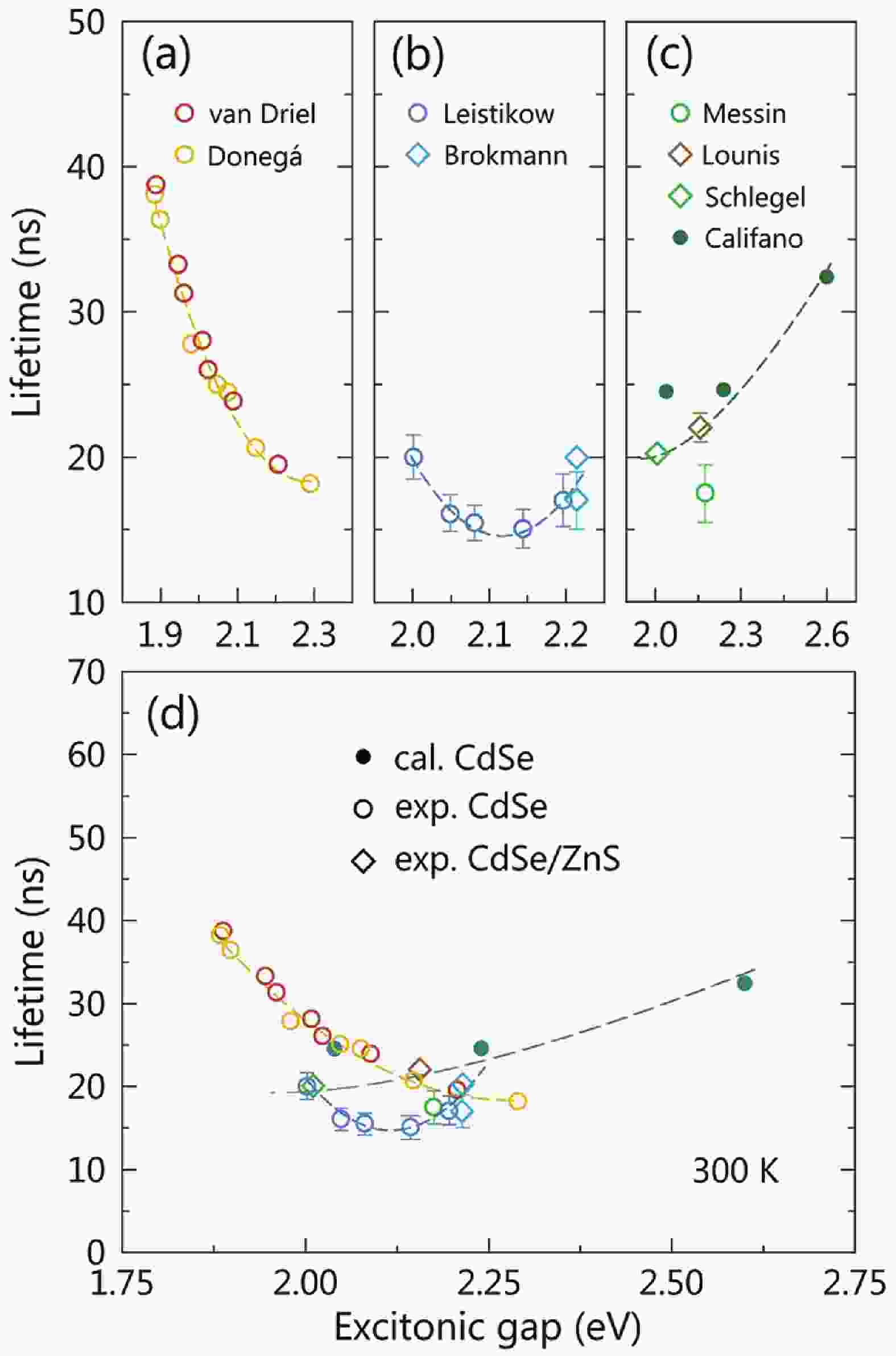
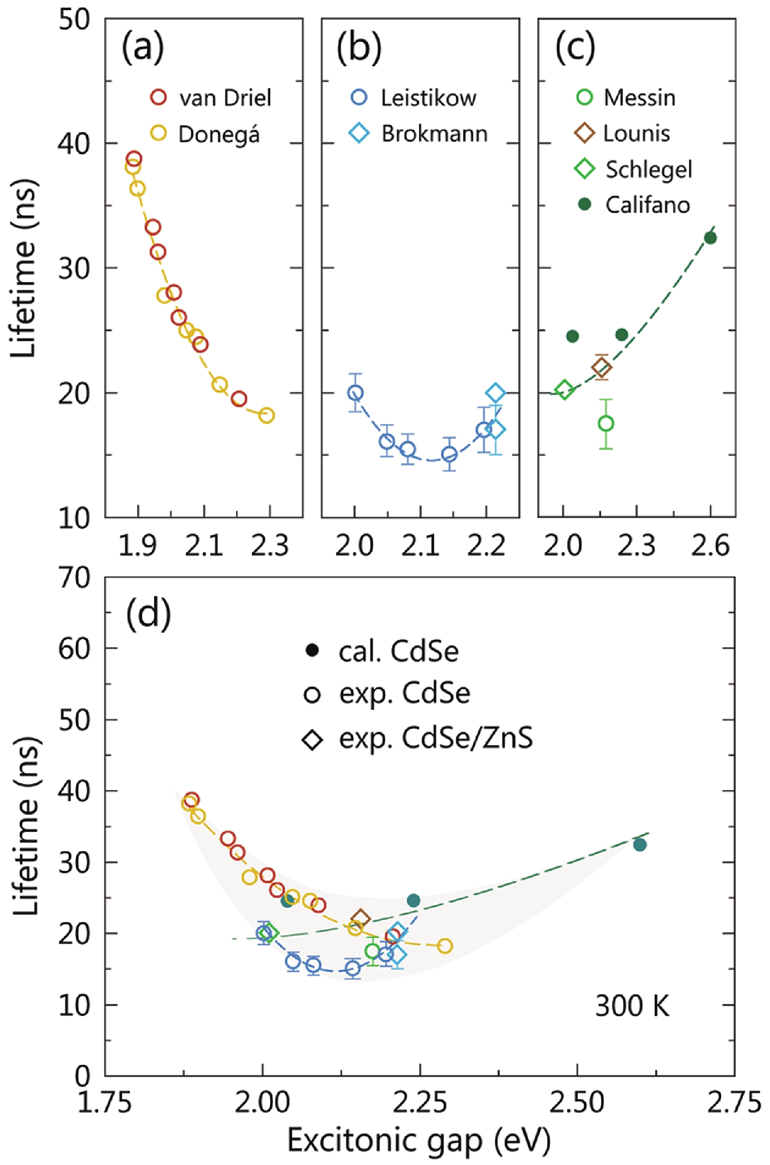
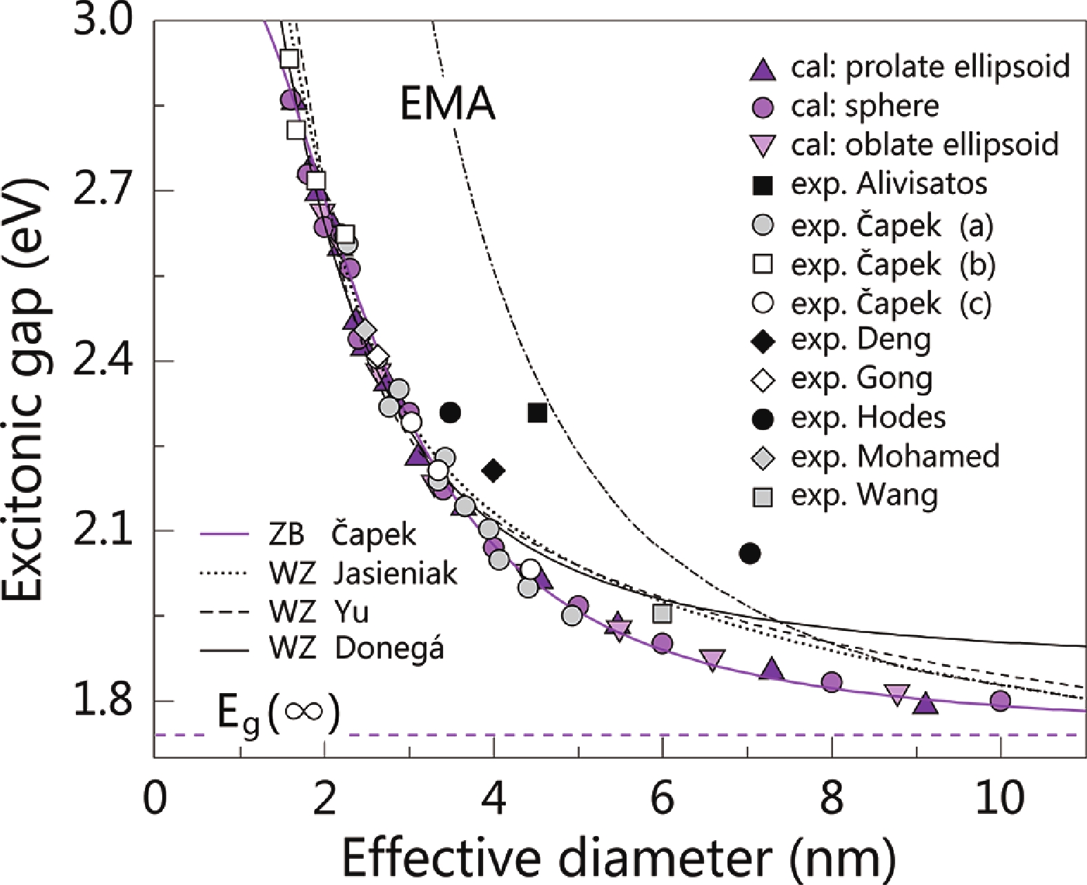
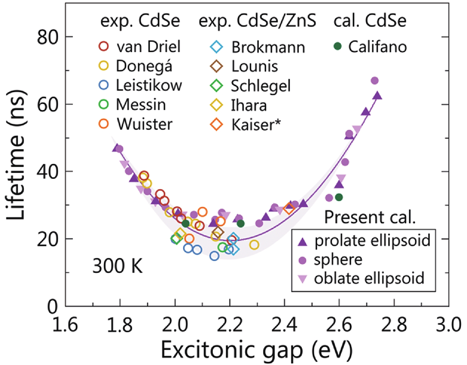
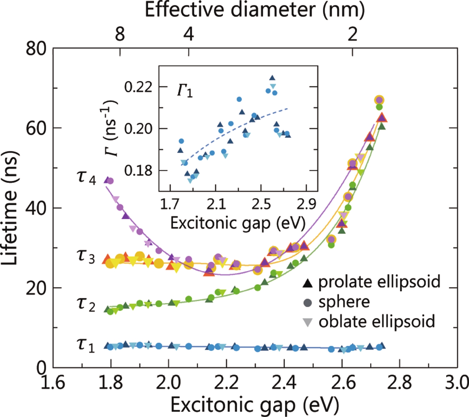
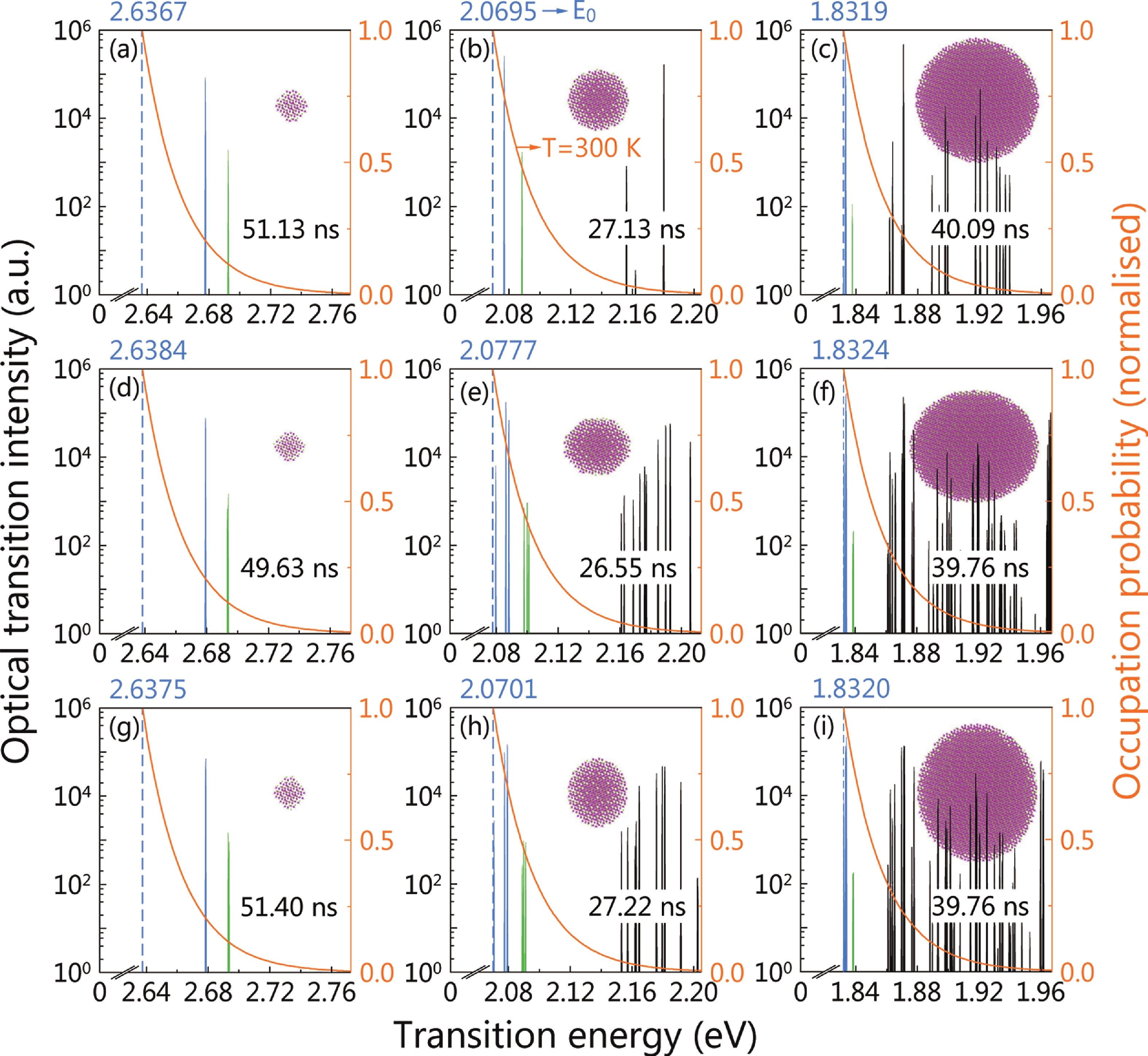
Colloidal CdSe quantum dots (QDs) are promising materials for solar cells because of their simple preparation process and compatibility with flexible substrates. The QD radiative recombination lifetime has attracted enormous attention as it affects the probability of photogenerated charges leaving the QDs and being collected at the battery electrodes. However, the scaling law for the exciton radiative lifetime in CdSe QDs is still a puzzle. This article presents a novel explanation that reconciles this controversy. Our calculations agree with the experimental measurements of all three divergent trends in a broadened energy window. Further, we proved that the exciton radiative lifetime is a consequence of the thermal average of decays for all thermally accessible exciton states. Each of the contradictory size-dependent patterns reflects this trend in a specific size range. As the optical band gap increases, the radiative lifetime decreases in larger QDs, increases in smaller QDs, and is weakly dependent on size in the intermediate energy region. This study addresses the inconsistencies in the scaling law of the exciton lifetime and gives a unified interpretation over a widened framework. Moreover, it provides valuable guidance for carrier separation in the thin film solar cell of CdSe QDs.

J. Semicond.
2023, 44(3): 032801 doi: 10.1088/1674-4926/44/3/032801
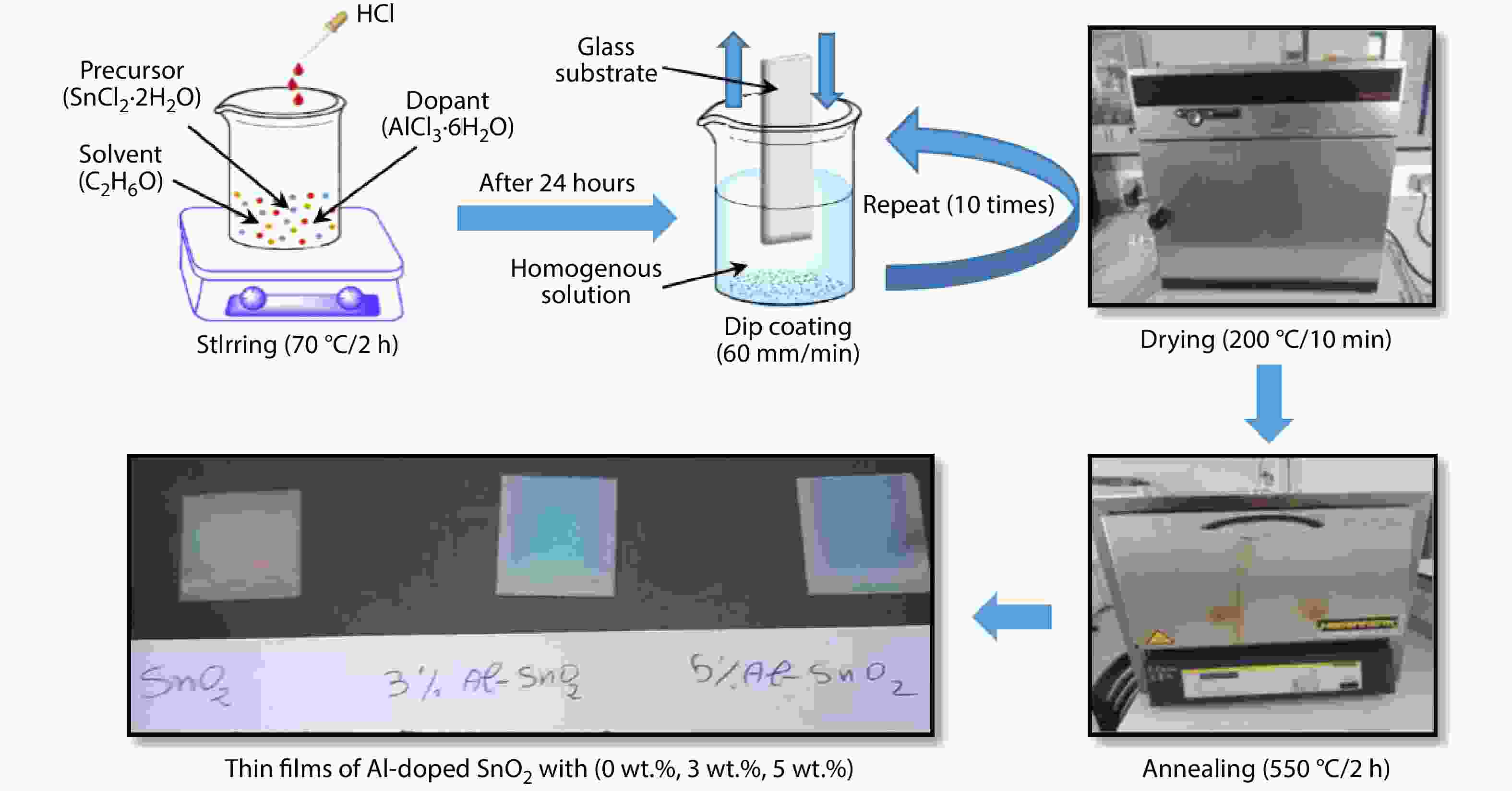
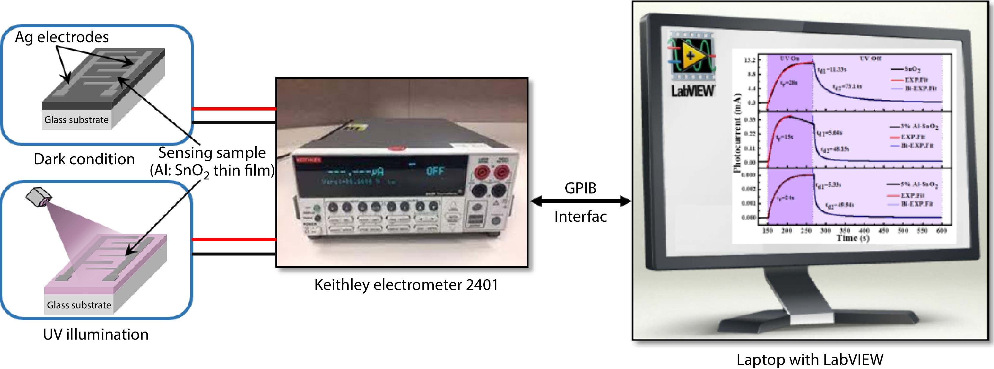
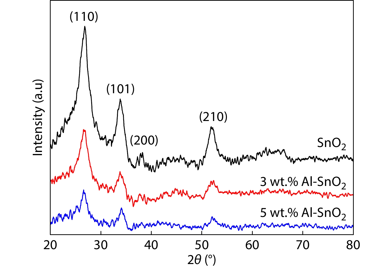
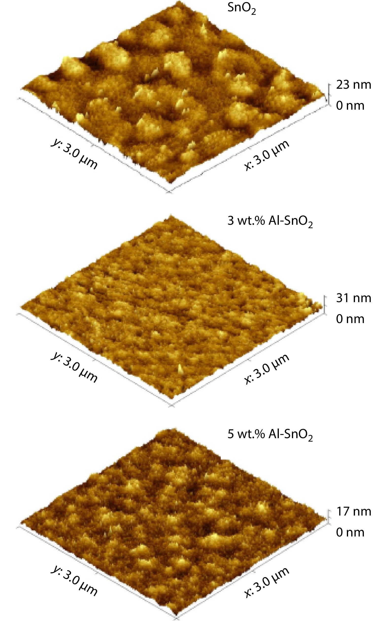
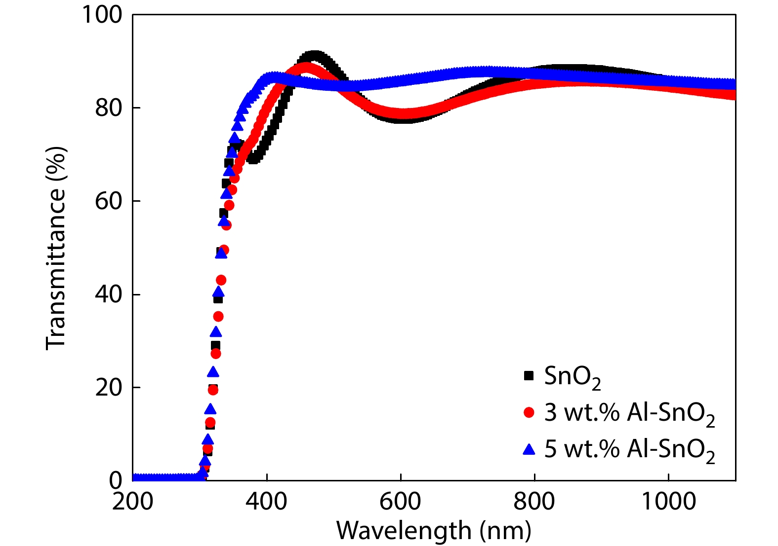
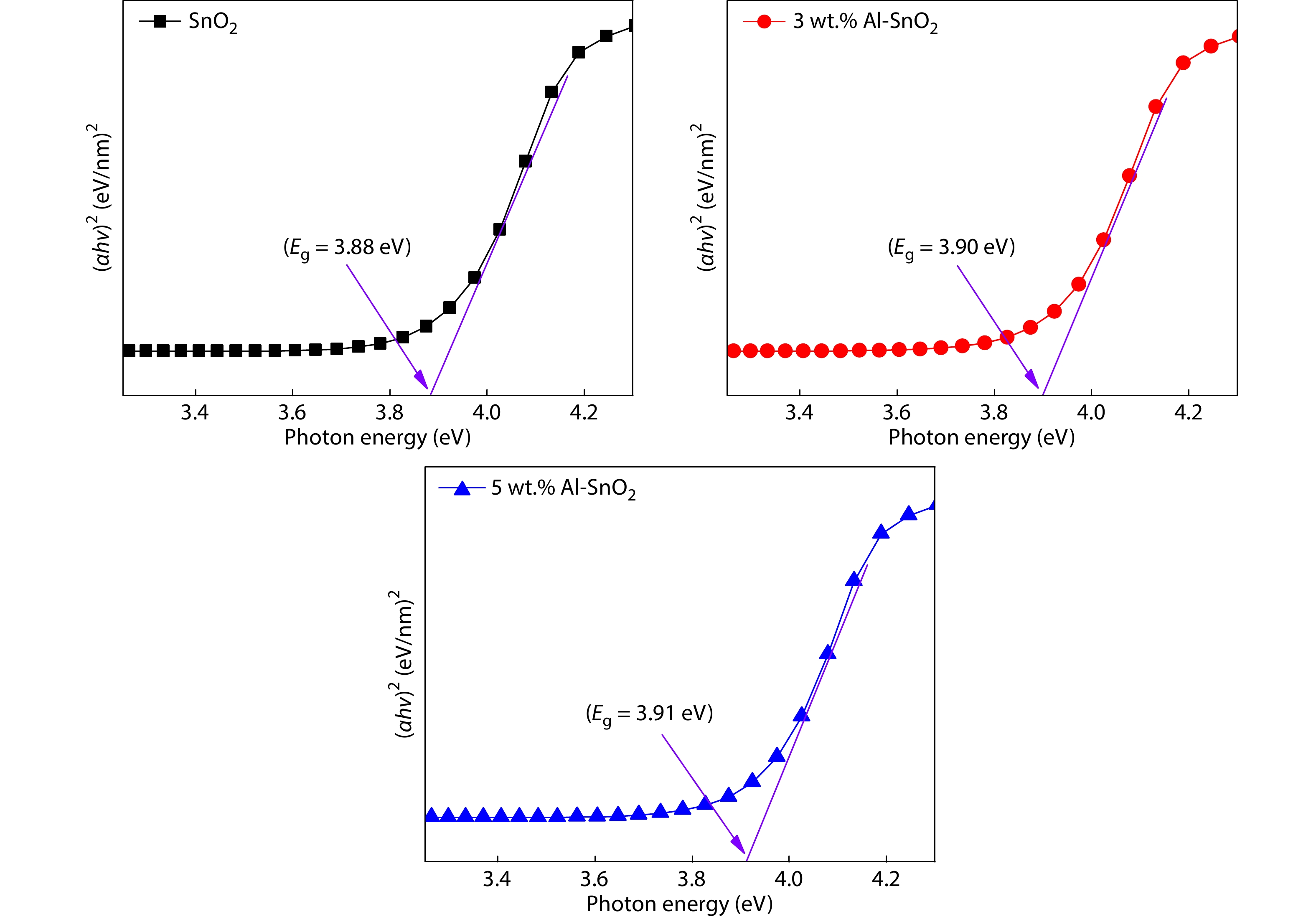
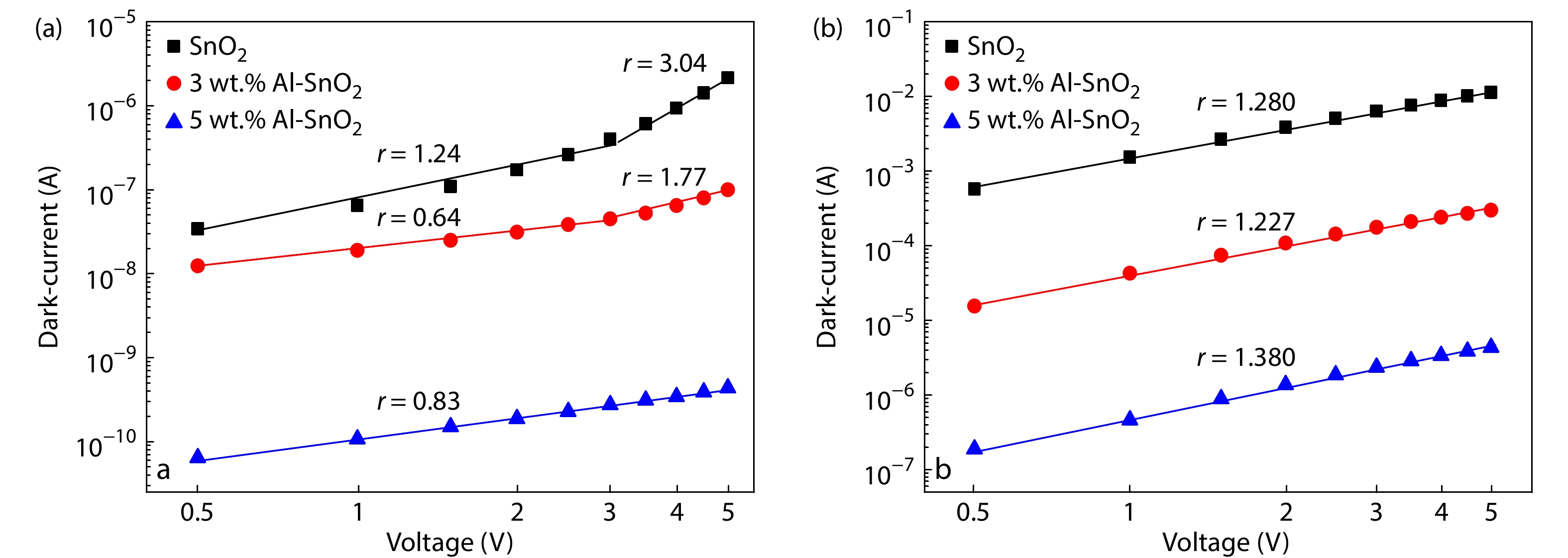
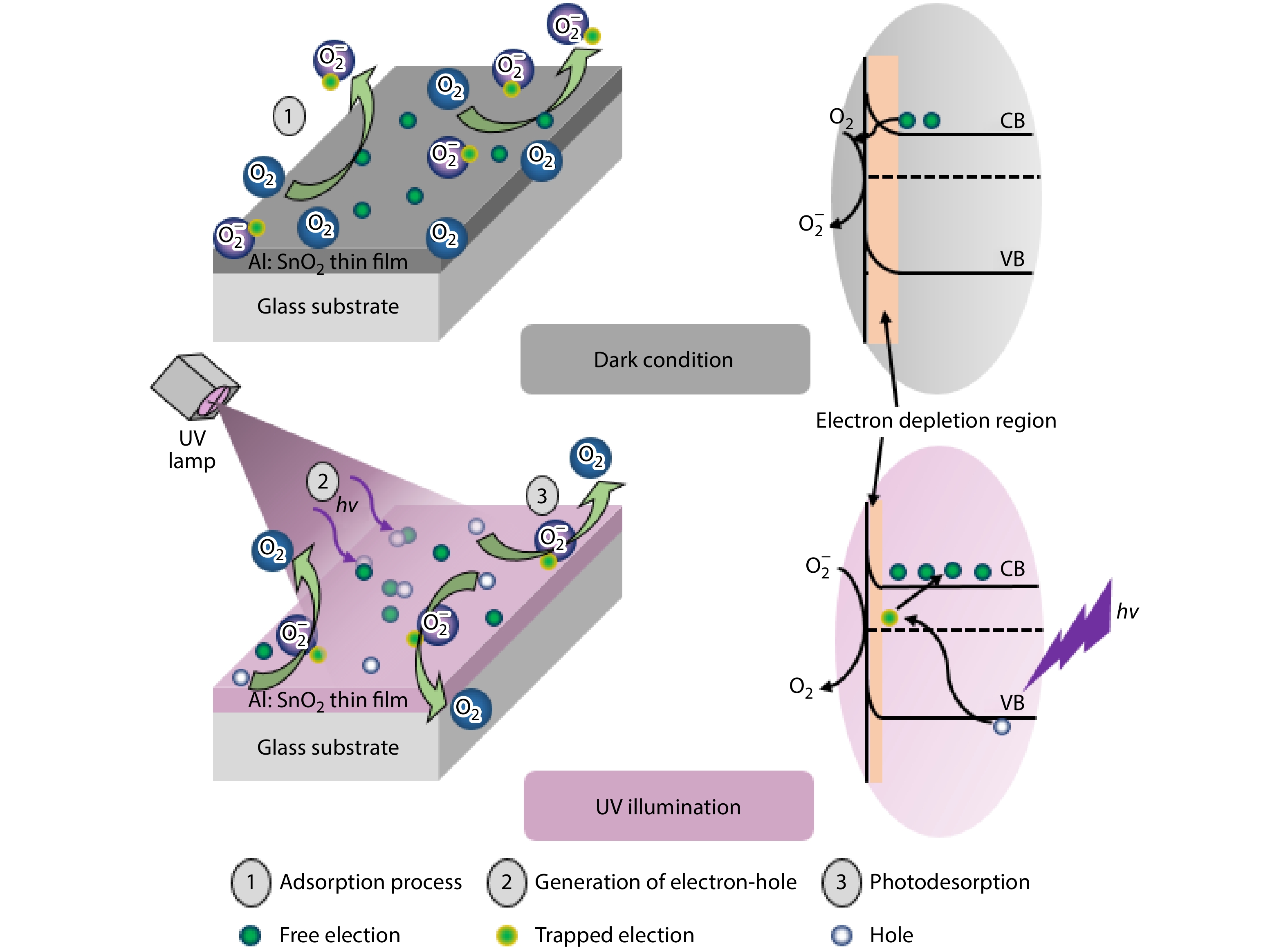
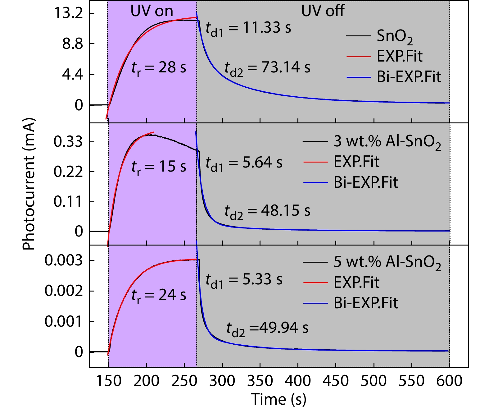
Transparent conducting aluminum doped tin oxide thin films were prepared by sol-gel dip coating method with different Al concentrations and characterized by X-ray diffraction (XRD), atomic force microscopy (AFM), UV–Vis spectrophotometry and photoconductivity study. The variation observed in the properties of the measured films agrees with a difference in the film's thickness, which decreases when Al concentration augments. X-ray diffraction analysis reveals that all films are polycrystalline with tetragonal structure, (110) plane being the strongest diffraction peak. The crystallite size calculated by the Debye Scherrer’s formula decreases from 11.92 to 8.54 nm when Al concentration increases from 0 to 5 wt.%. AFM images showed grains uniformly distributed in the deposited films. An average transmittance greater than 80% was measured for the films and an energy gap value of about 3.9 eV was deduced from the optical analysis. Finally, the photosensitivity properties like current–voltage characteristics, ION/IOFF ratio, growth and decay time are studied and reported. Also, we have calculated the trap depth energy using the decay portion of the rise and decay curve photocurrent.