Issue Browser
Volume 44, Issue 7,
Jul 2023
J. Semicond.
2023, 44(7): 071801 doi: 10.1088/1674-4926/44/7/071801
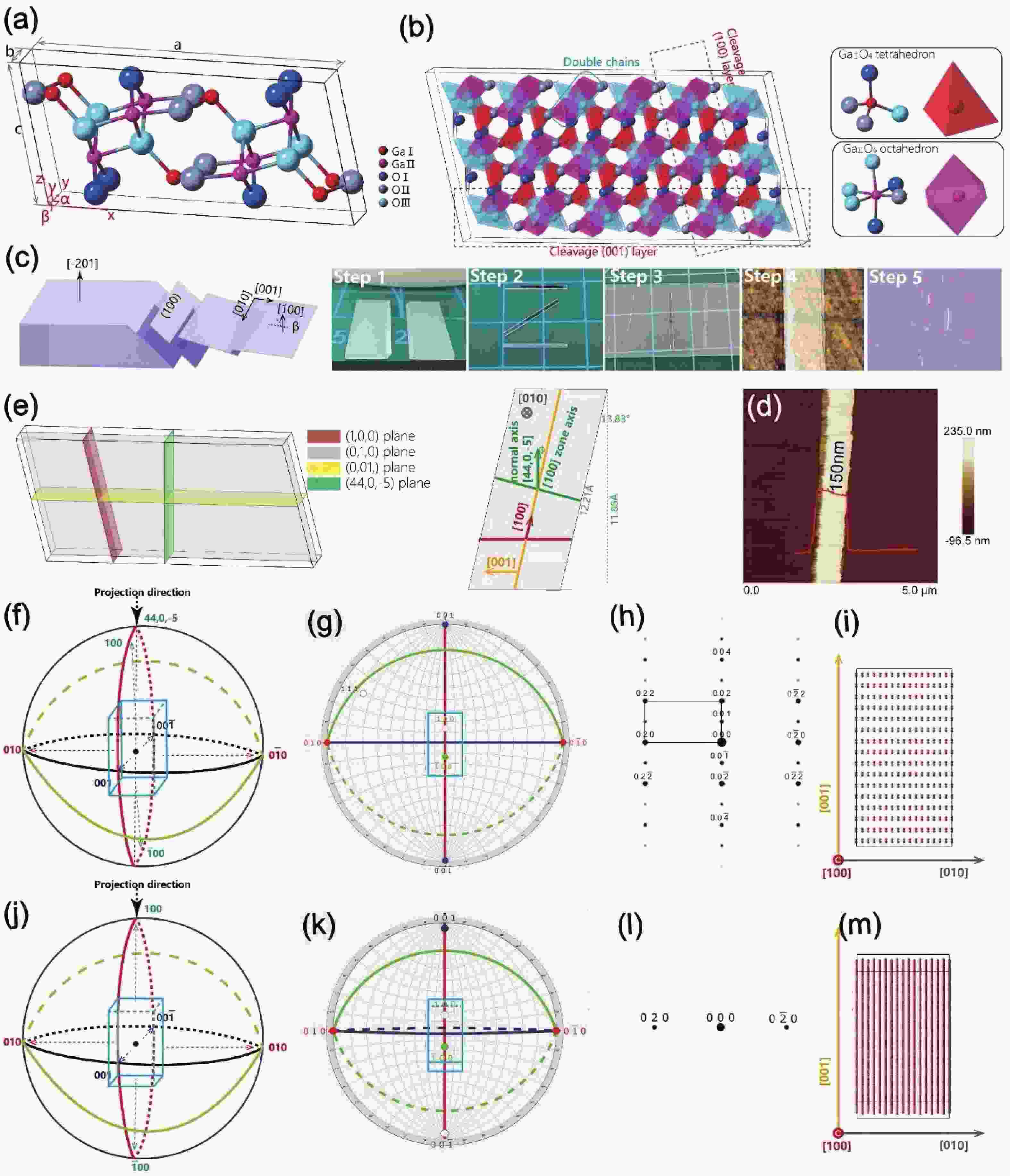
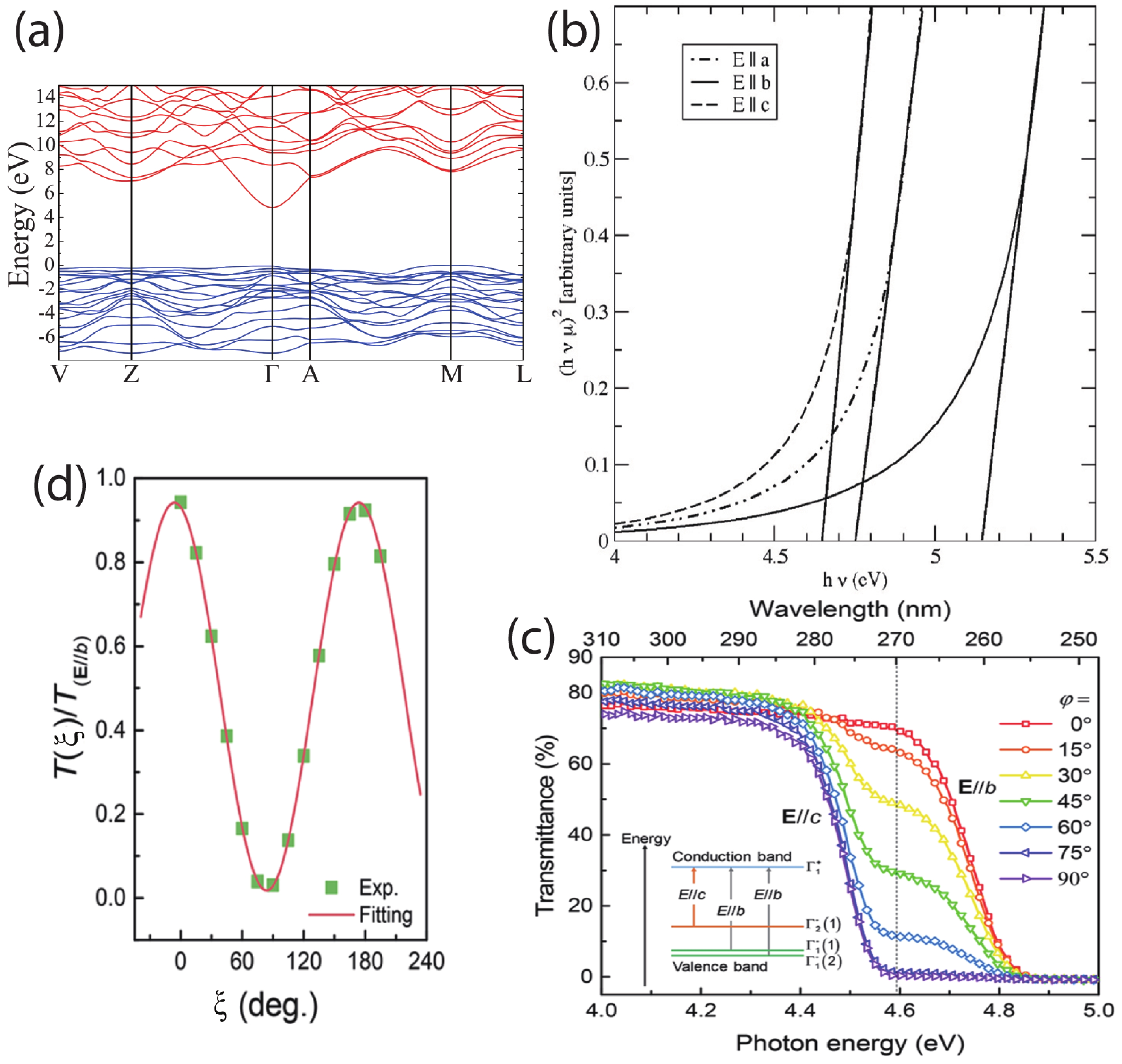
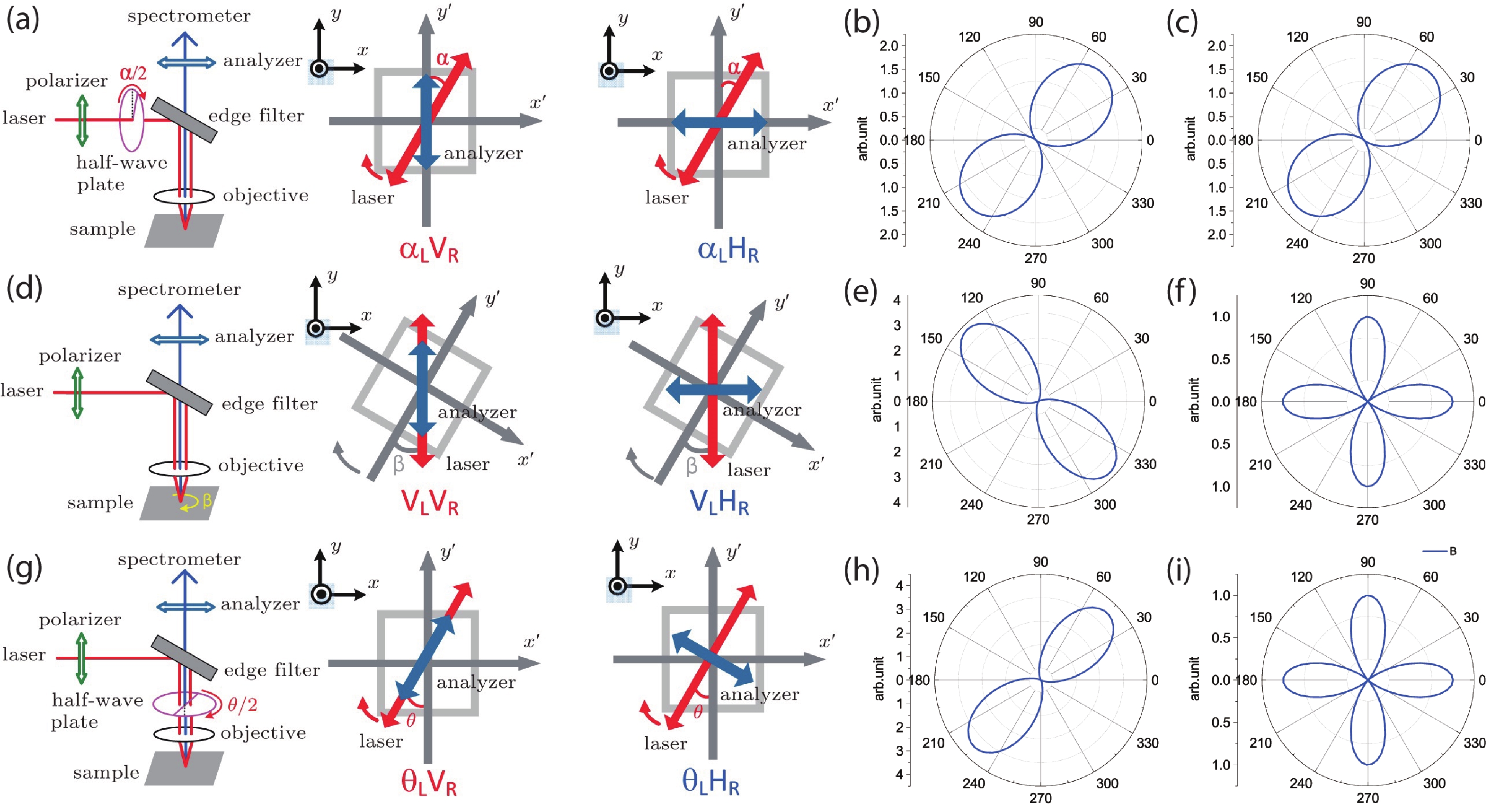
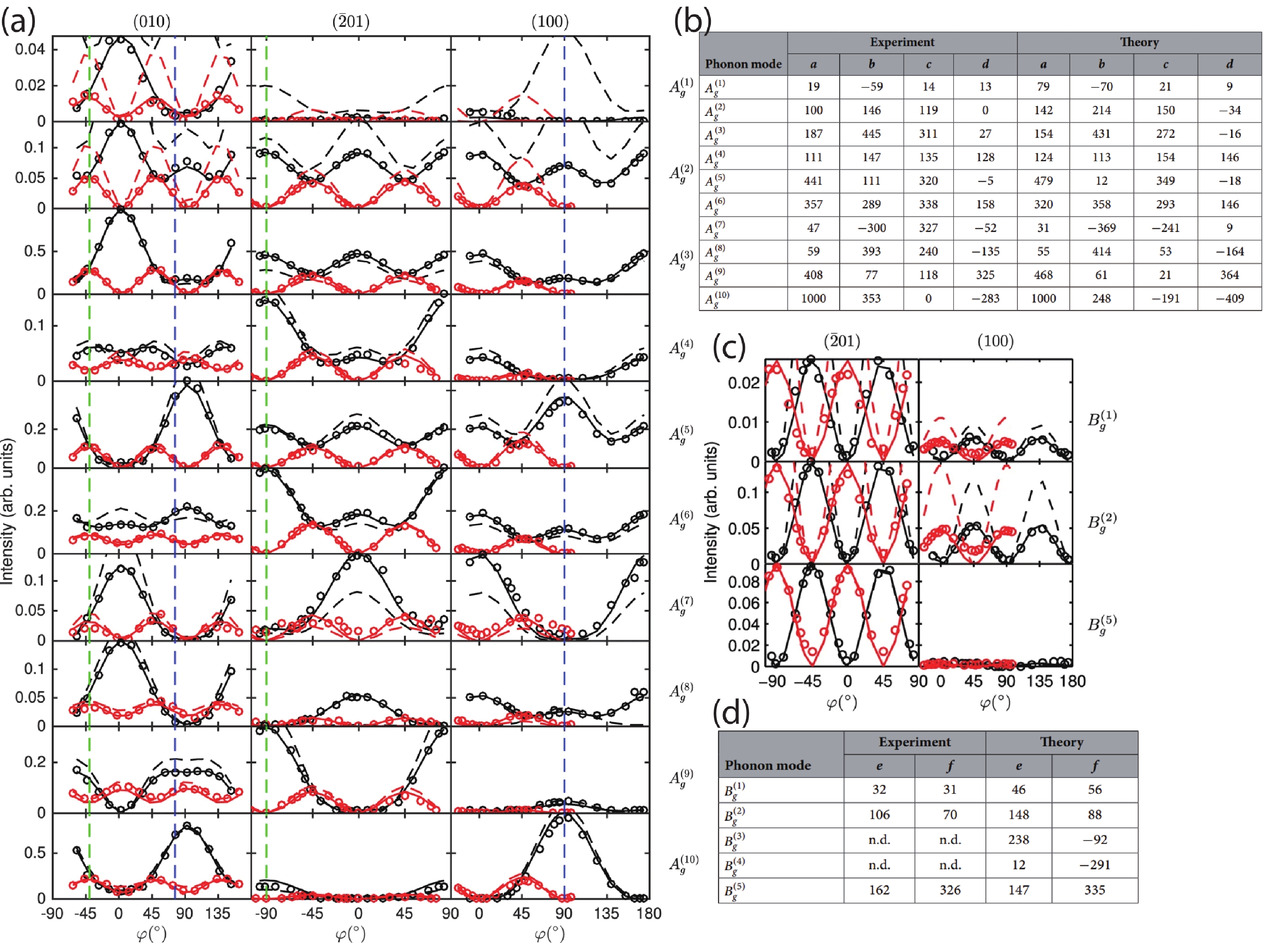
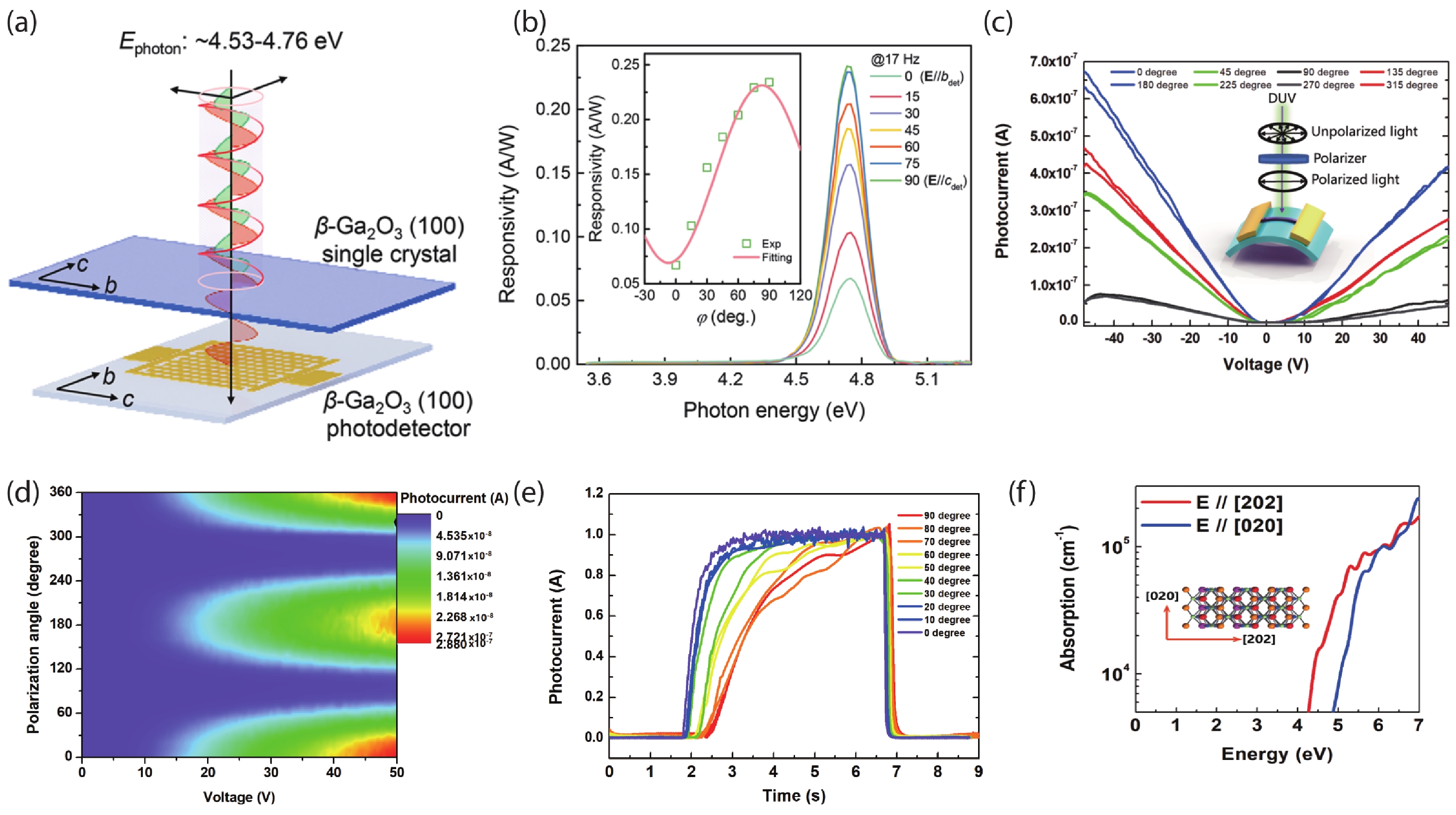
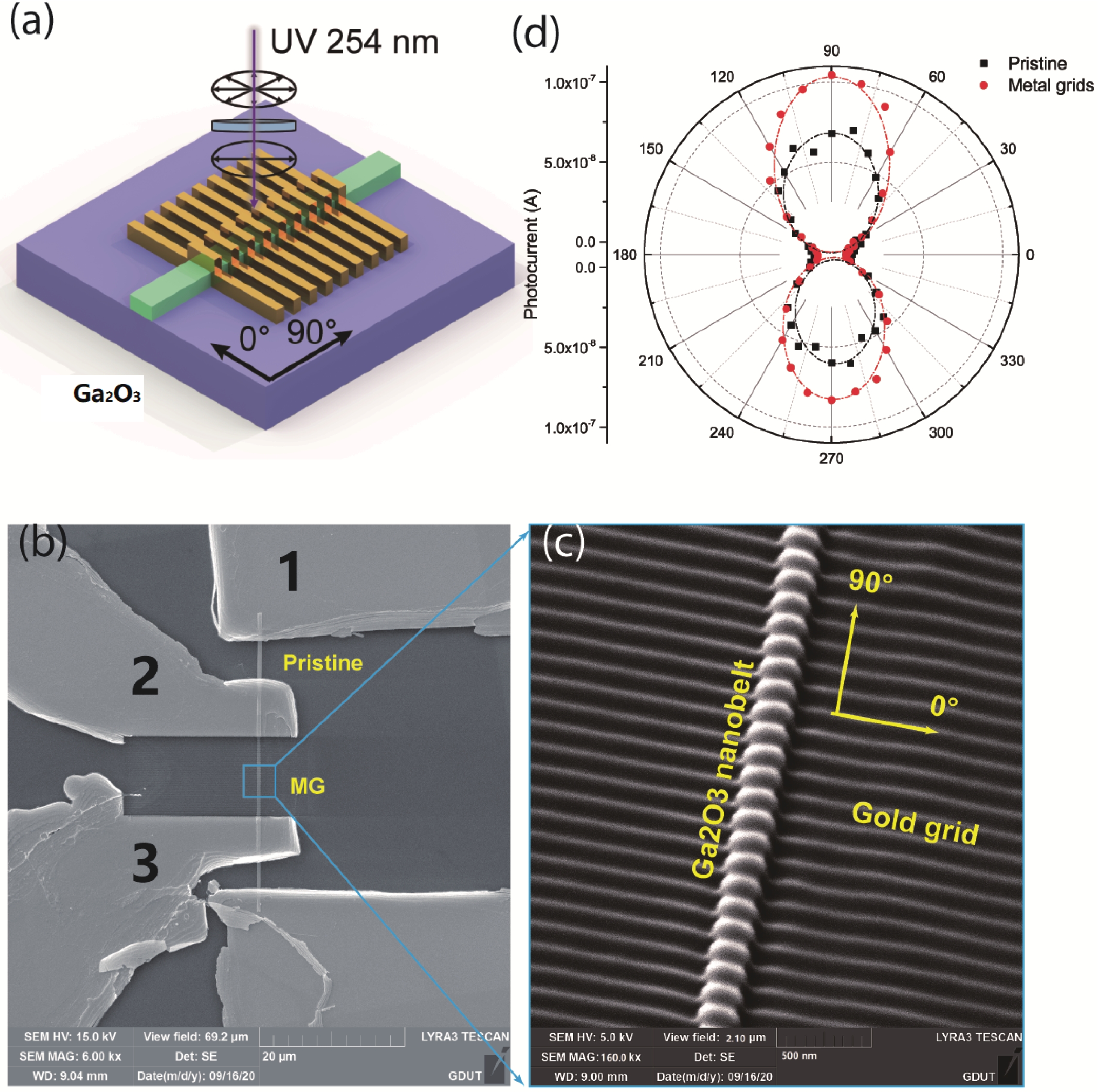
The anisotropic properties and applications of β-gallium oxide (β-Ga2O3) are comprehensively reviewed. All the anisotropic properties are essentially resulted from the anisotropic crystal structure. The process flow of how to exfoliate nanoflakes from bulk material is introduced. Anisotropic optical properties, including optical bandgap, Raman and photoluminescence characters are comprehensively reviewed. Three measurement configurations of angle-resolved polarized Raman spectra (ARPRS) are reviewed, with Raman intensity formulas calculated with Raman tensor elements. The method to obtain the Raman tensor elements of phonon modes through experimental fitting is also introduced. In addition, the anisotropy in electron mobility and affinity are discussed. The applications, especially polarization photodetectors, based on β-Ga2O3 were summarized comprehensively. Three kinds of polarization detection mechanisms based on material dichroism, 1D morphology and metal-grids are discussed in-depth. This review paper provides a framework for anisotropic optical and electric properties of β-Ga2O3, as well as the applications based on these characters, and is expected to lead to a wider discussion on this topic.


J. Semicond.
2023, 44(7): 072801 doi: 10.1088/1674-4926/44/7/072801
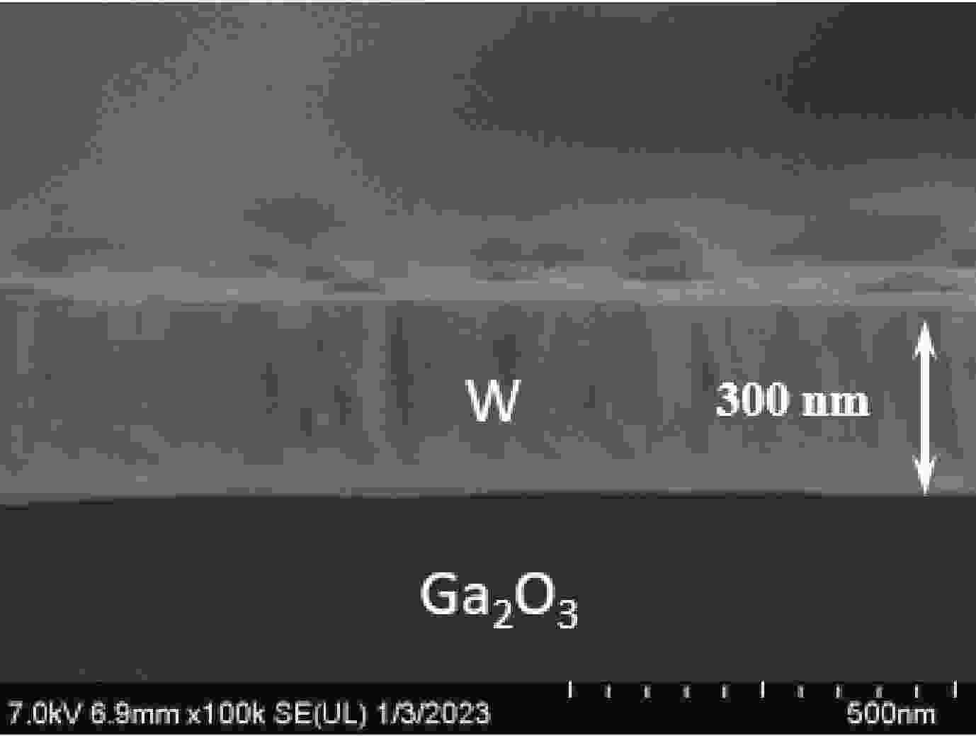
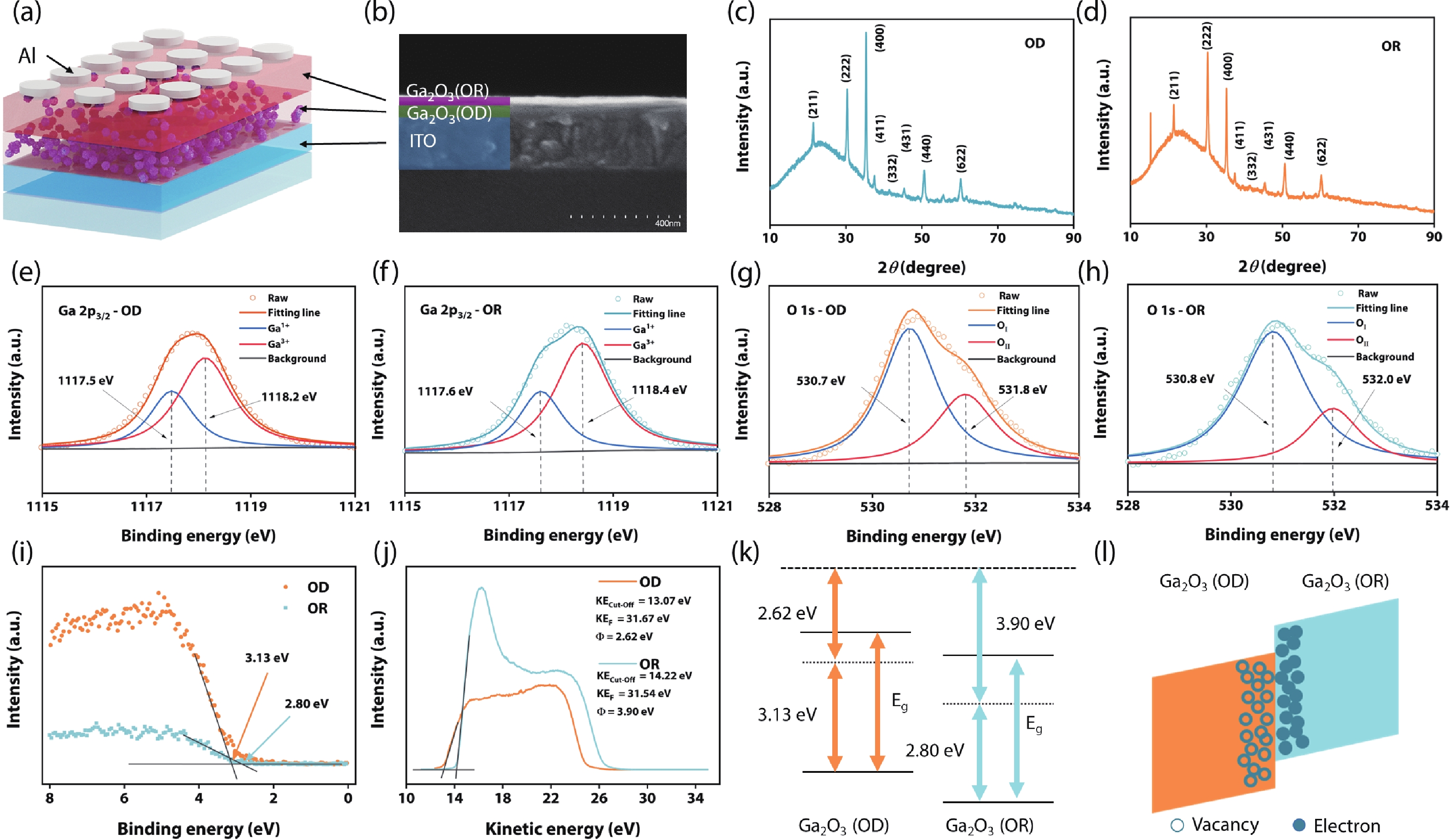
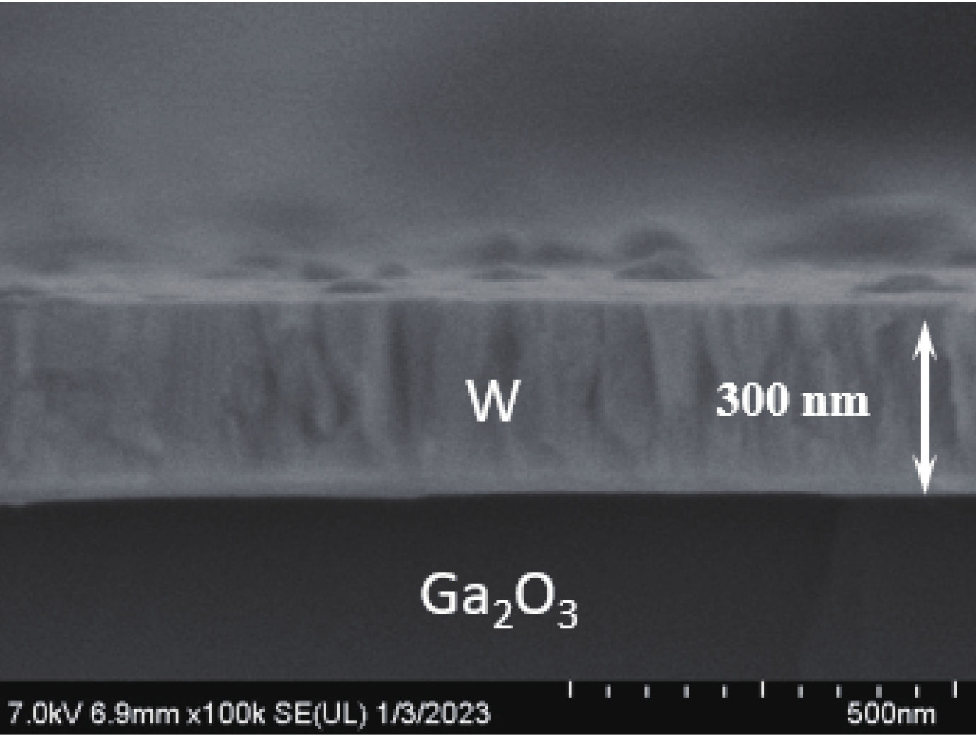
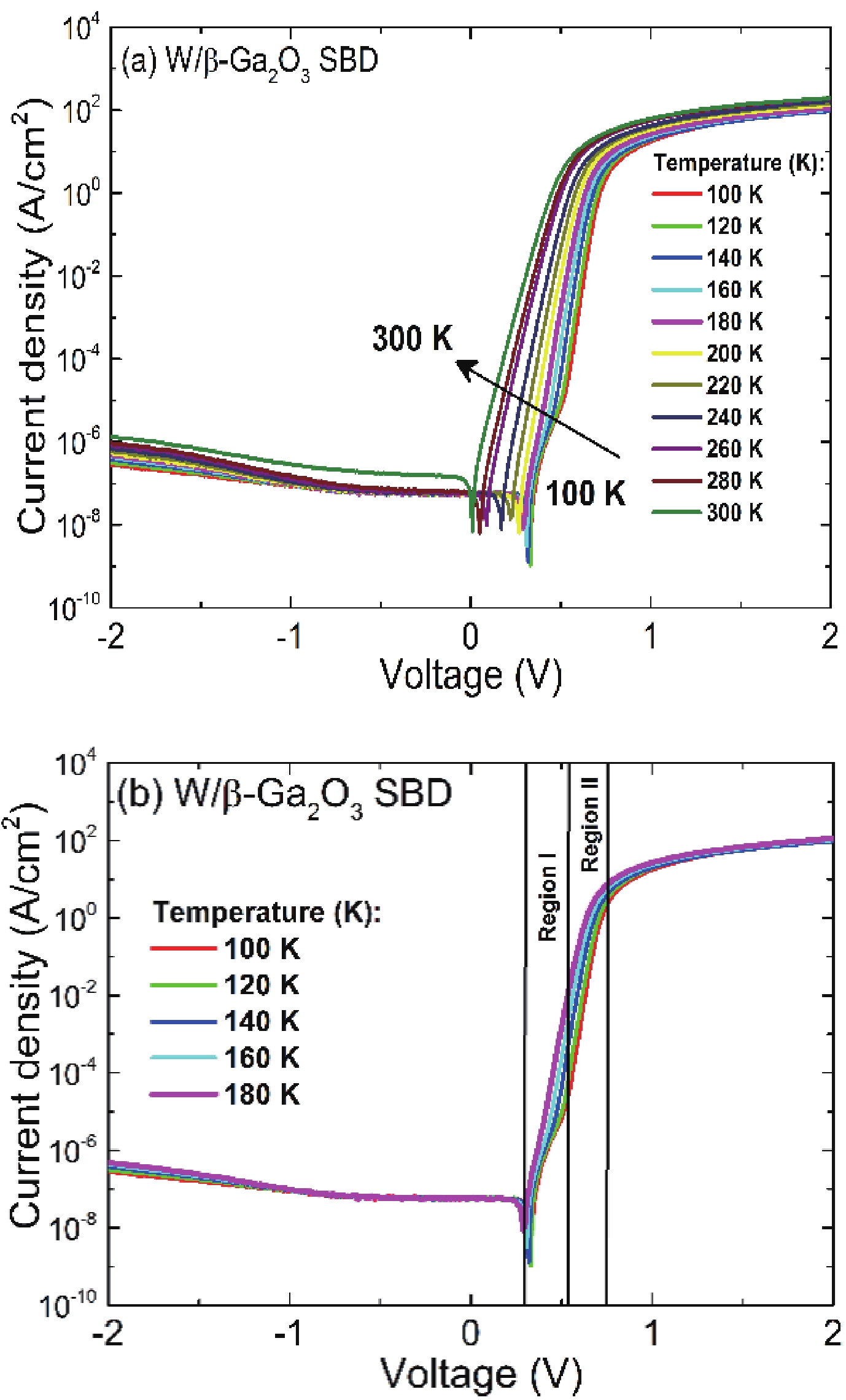
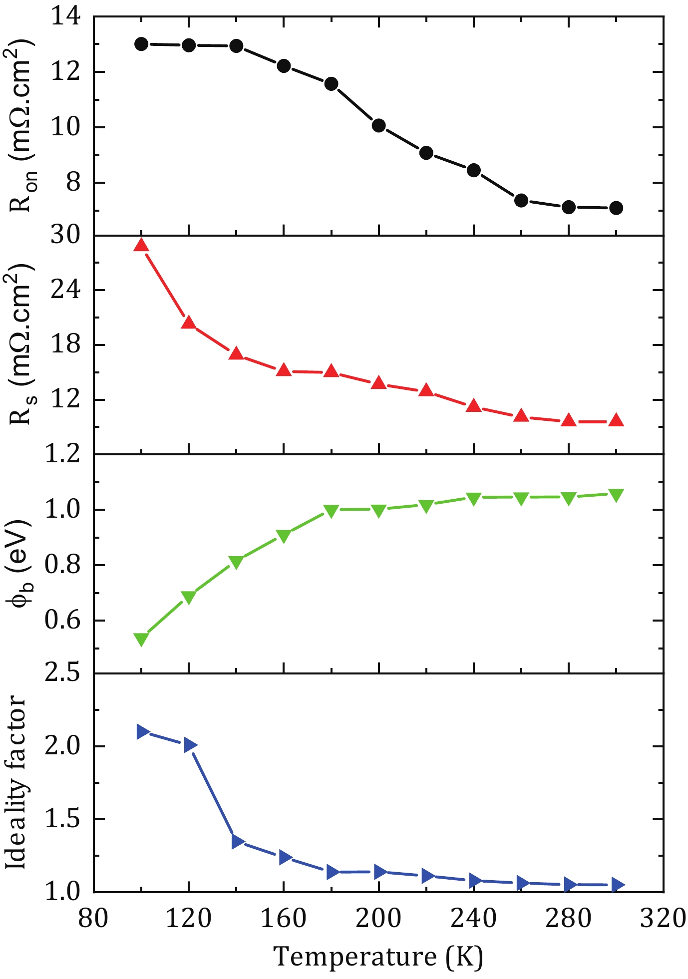
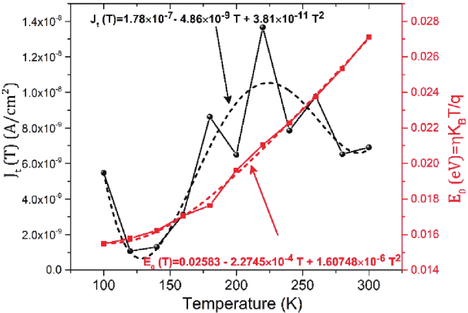
In this work, W/β-Ga2O3 Schottky barrier diodes, prepared using a confined magnetic field-based sputtering method, were analyzed at different operation temperatures. Firstly, Schottky barrier height increased with increasing temperature from 100 to 300 K and reached 1.03 eV at room temperature. The ideality factor decreased with increasing temperature and it was higher than 2 at 100 K. This apparent high value was related to the tunneling effect. Secondly, the series and on-resistances decreased with increasing operation temperature. Finally, the interfacial dislocation was extracted from the tunneling current. A high dislocation density was found, which indicates the domination of tunneling through dislocation in the transport mechanism. These findings are evidently helpful in designing better performance devices.

J. Semicond.
2023, 44(7): 072802 doi: 10.1088/1674-4926/44/7/072802
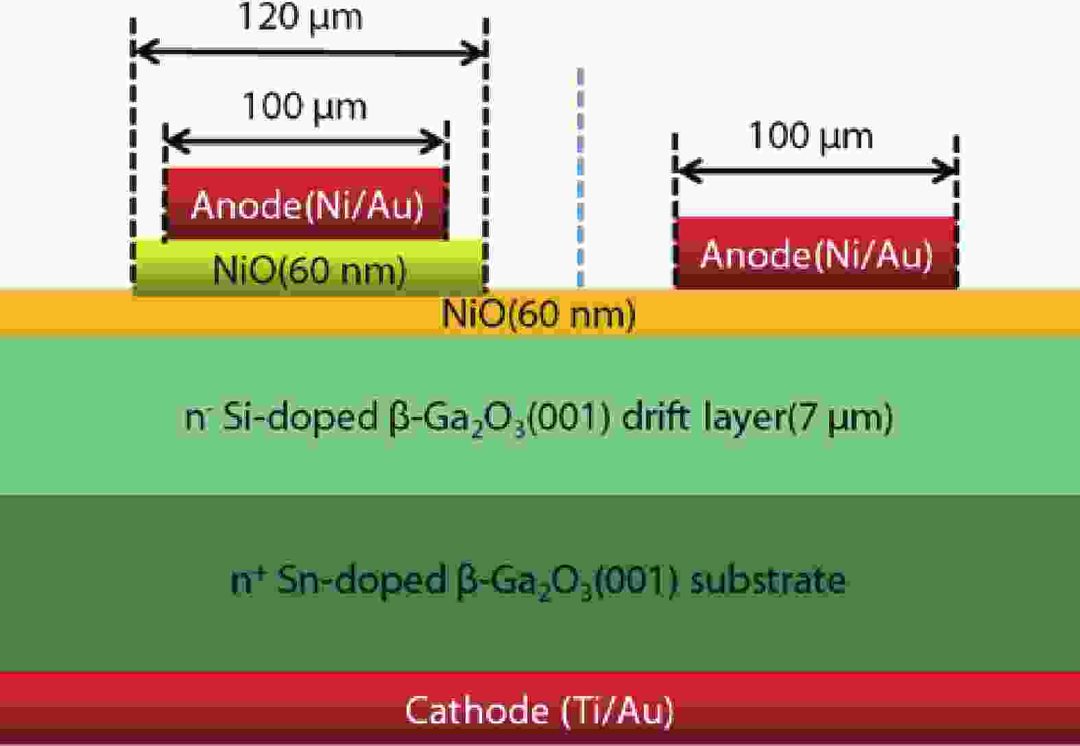
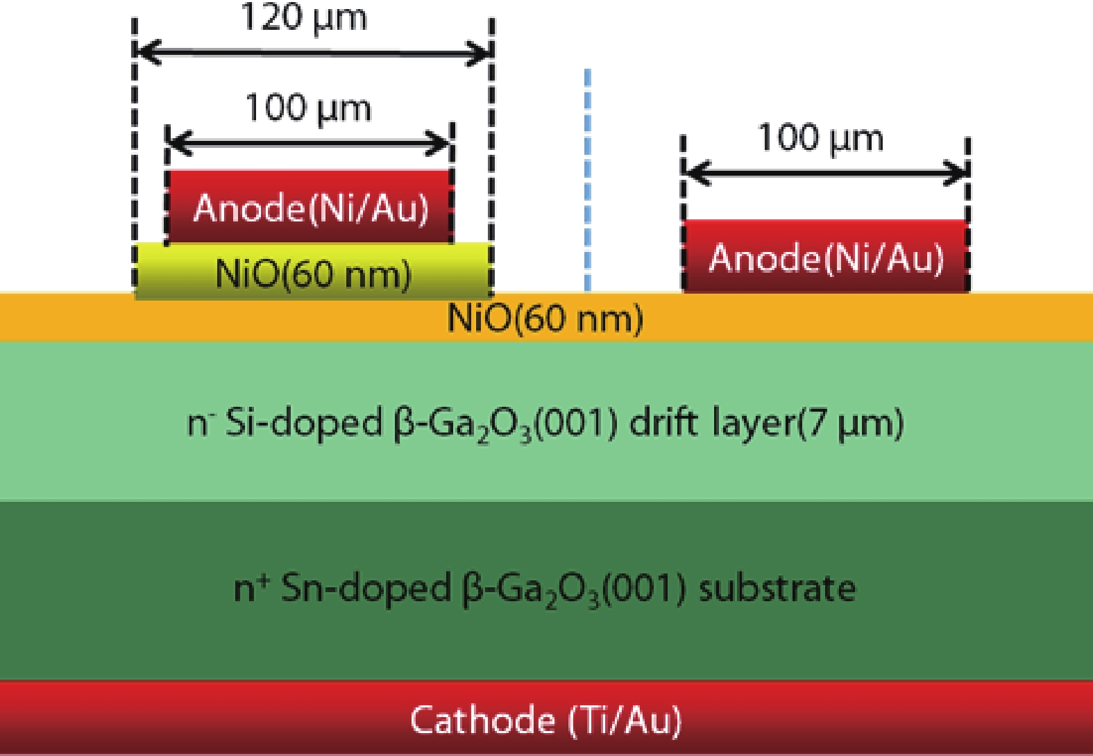
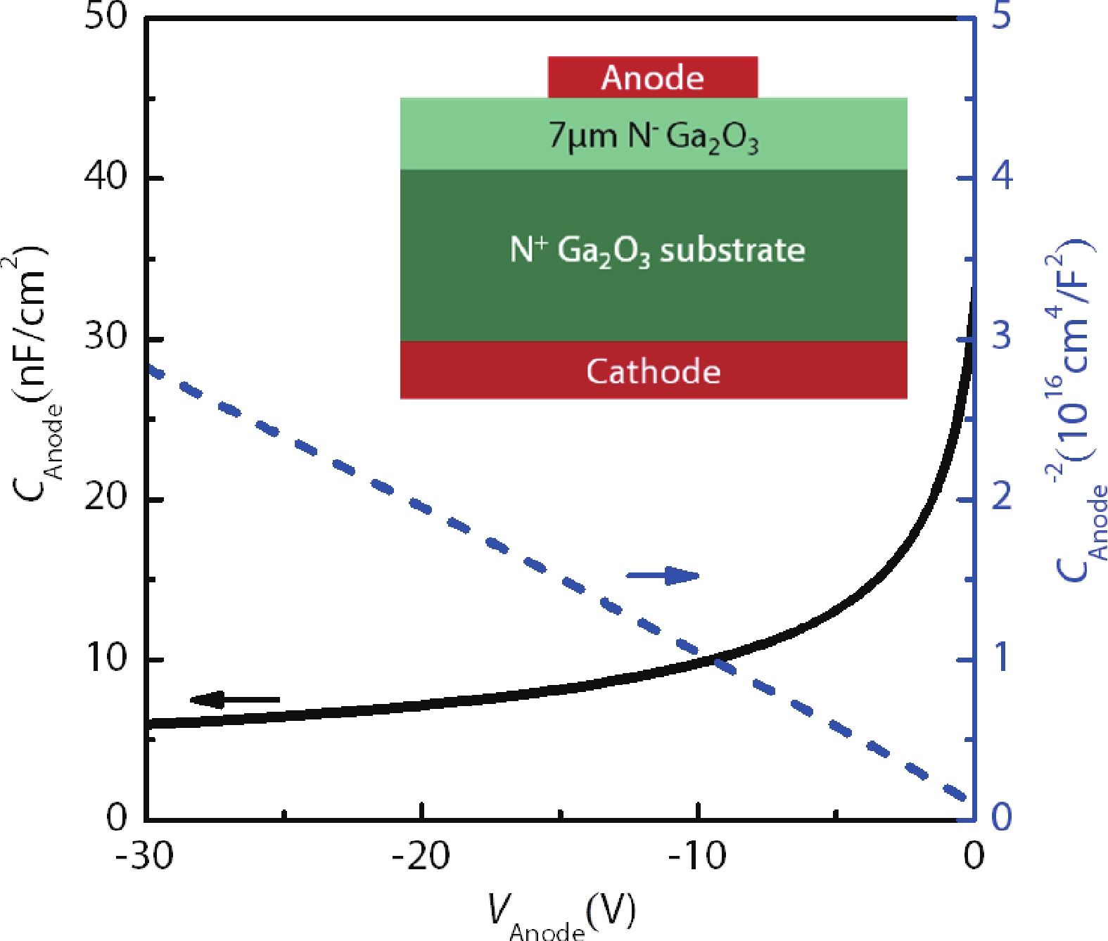
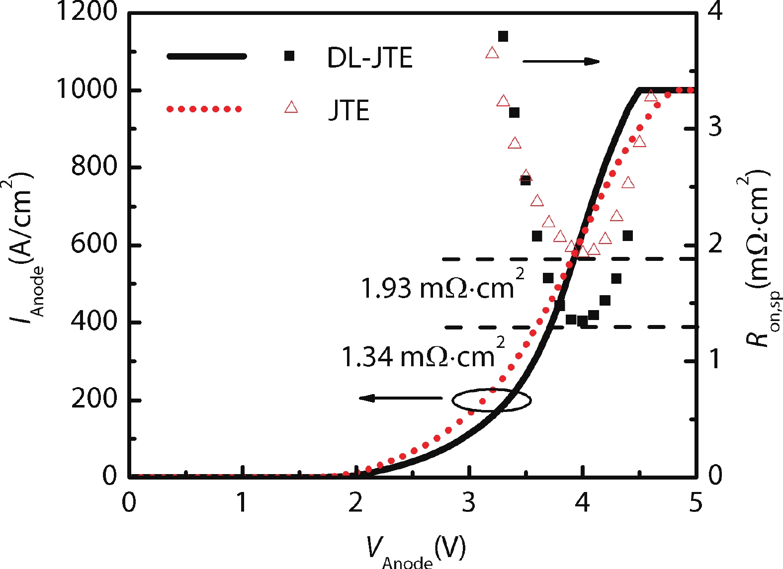
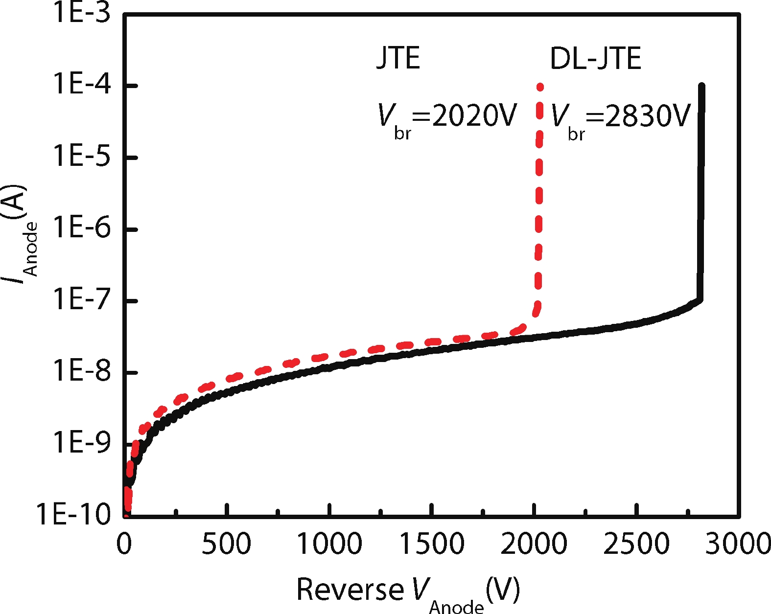
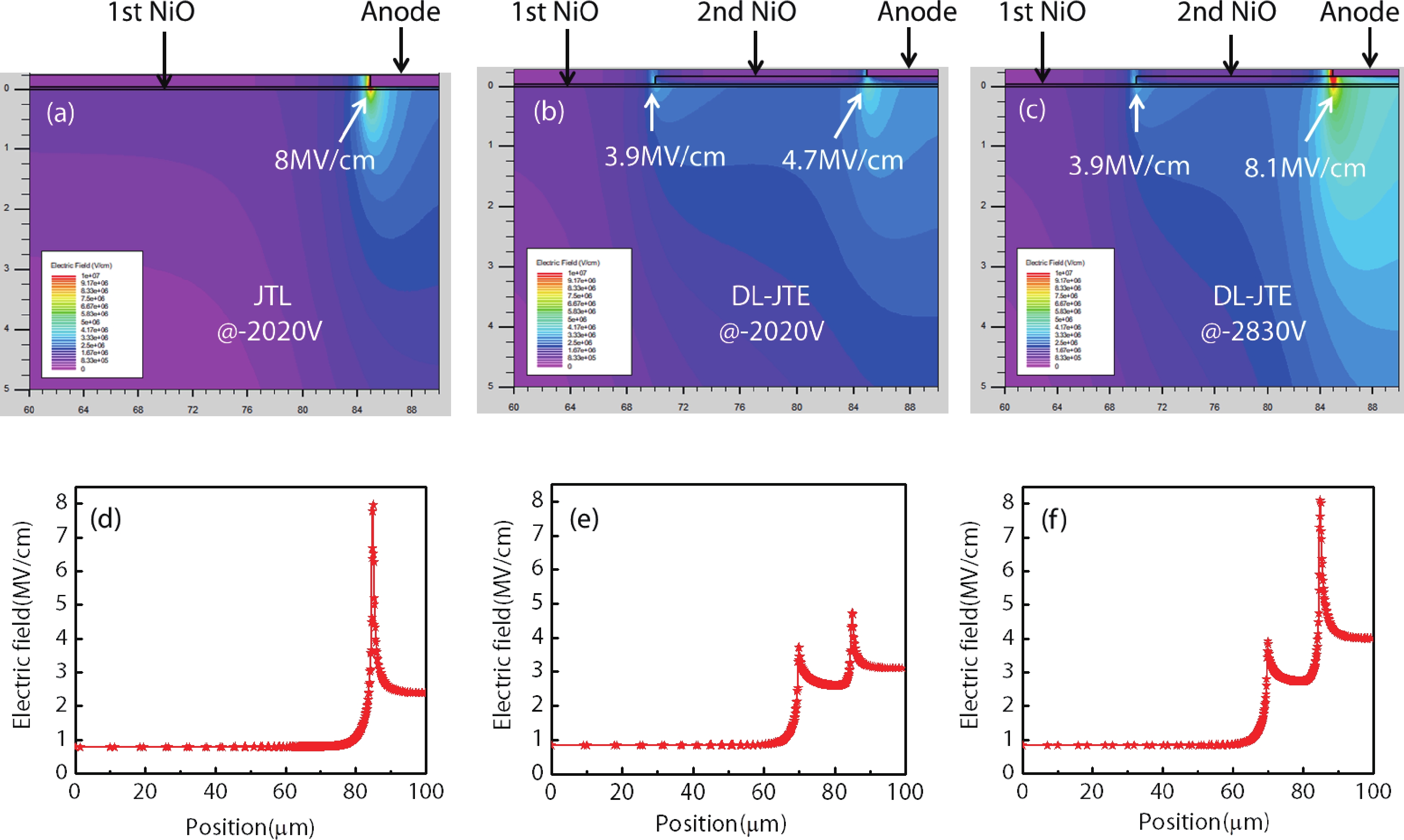
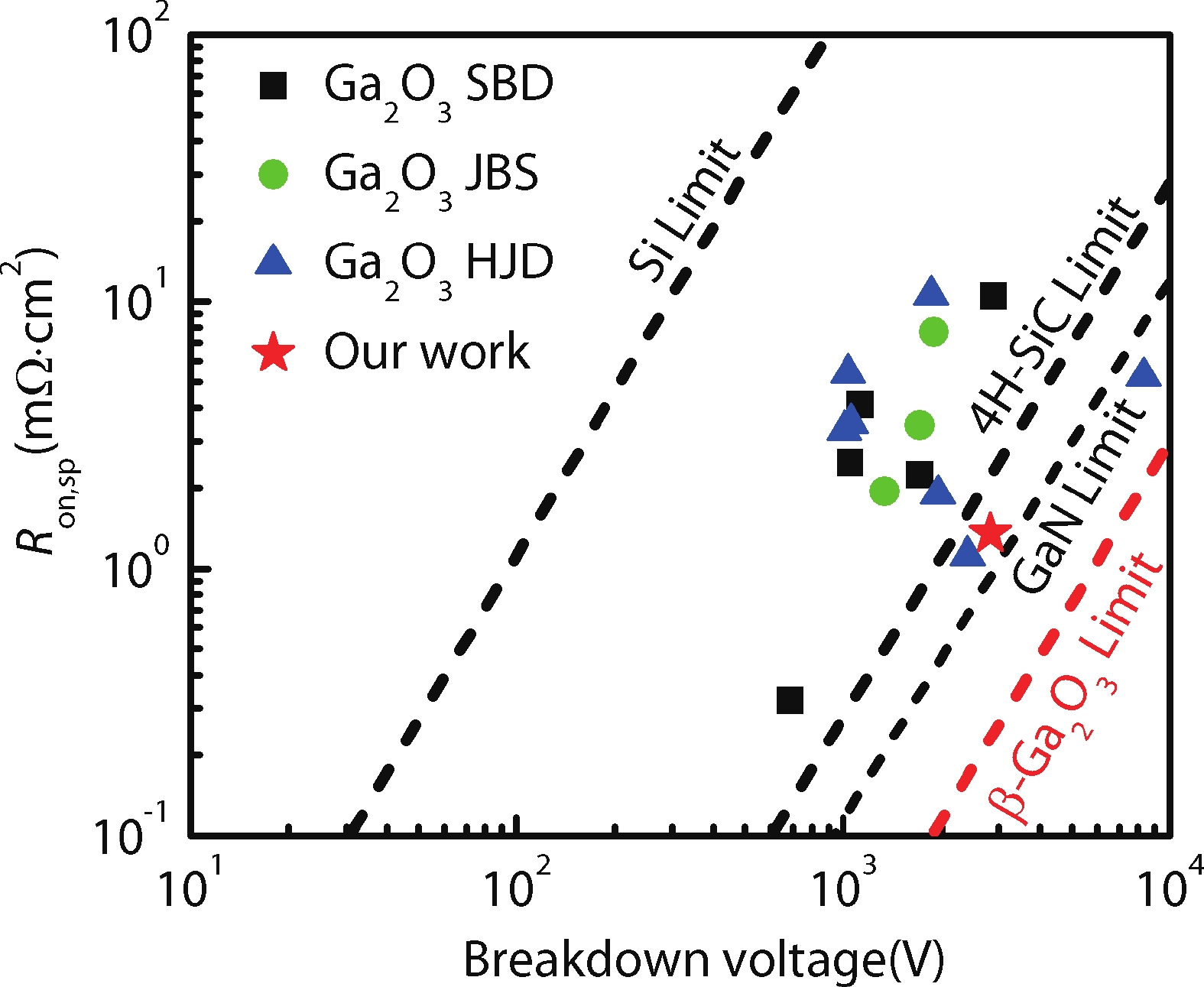
This work demonstrates high-performance NiO/β-Ga2O3 vertical heterojunction diodes (HJDs) with double-layer junction termination extension (DL-JTE) consisting of two p-typed NiO layers with varied lengths. The bottom 60-nm p-NiO layer fully covers the β-Ga2O3 wafer, while the geometry of the upper 60-nm p-NiO layer is 10 μm larger than the square anode electrode. Compared with a single-layer JTE, the electric field concentration is inhibited by double-layer JTE structure effectively, resulting in the breakdown voltage being improved from 2020 to 2830 V. Moreover, double p-typed NiO layers allow more holes into the Ga2O3 drift layer to reduce drift resistance. The specific on-resistance is reduced from 1.93 to 1.34 mΩ·cm2. The device with DL-JTE shows a power figure-of-merit (PFOM) of 5.98 GW/cm2, which is 2.8 times larger than that of the conventional single-layer JTE structure. These results indicate that the double-layer JTE structure provides a viable way of fabricating high-performance Ga2O3 HJDs.
J. Semicond.
2023, 44(7): 072803 doi: 10.1088/1674-4926/44/7/072803
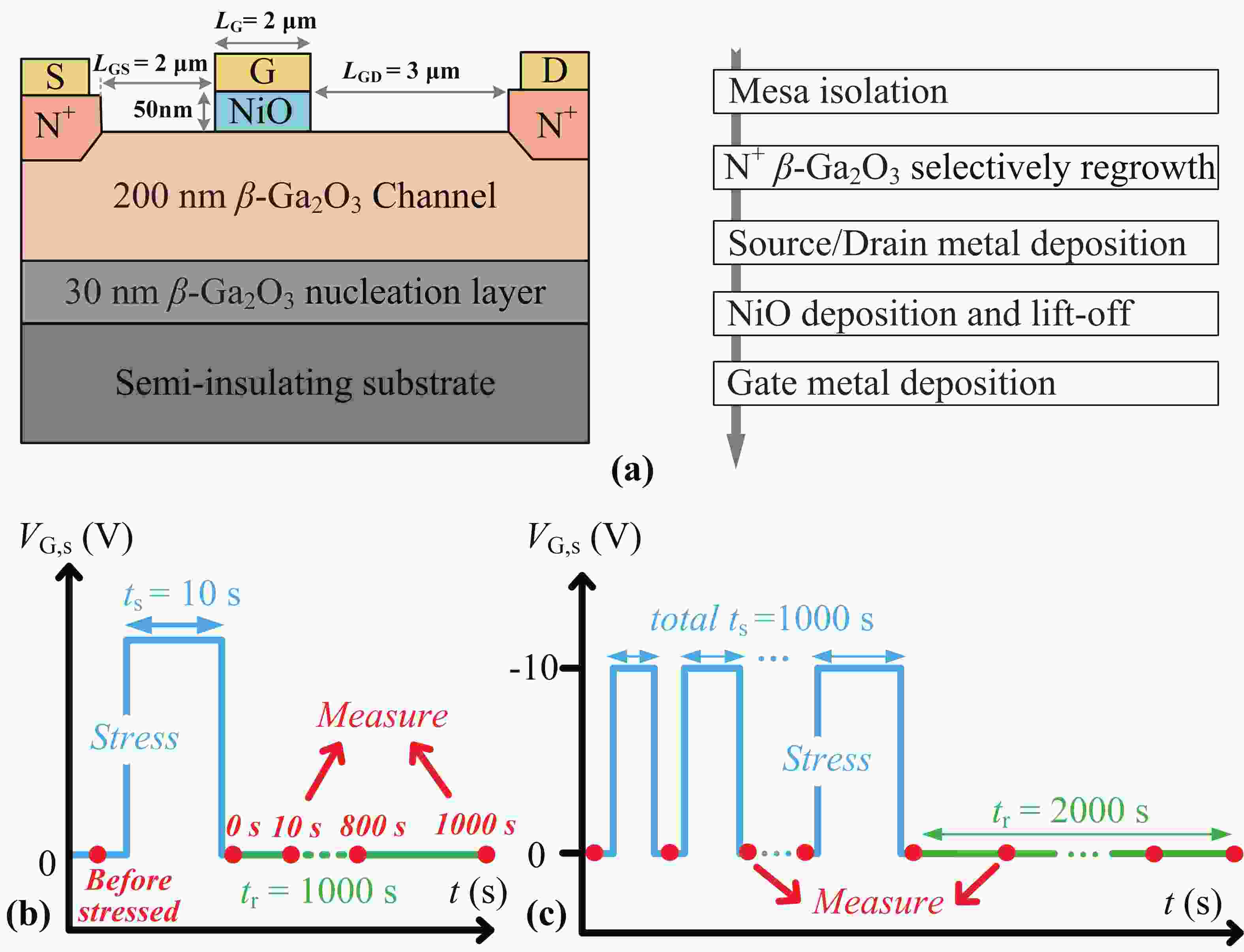
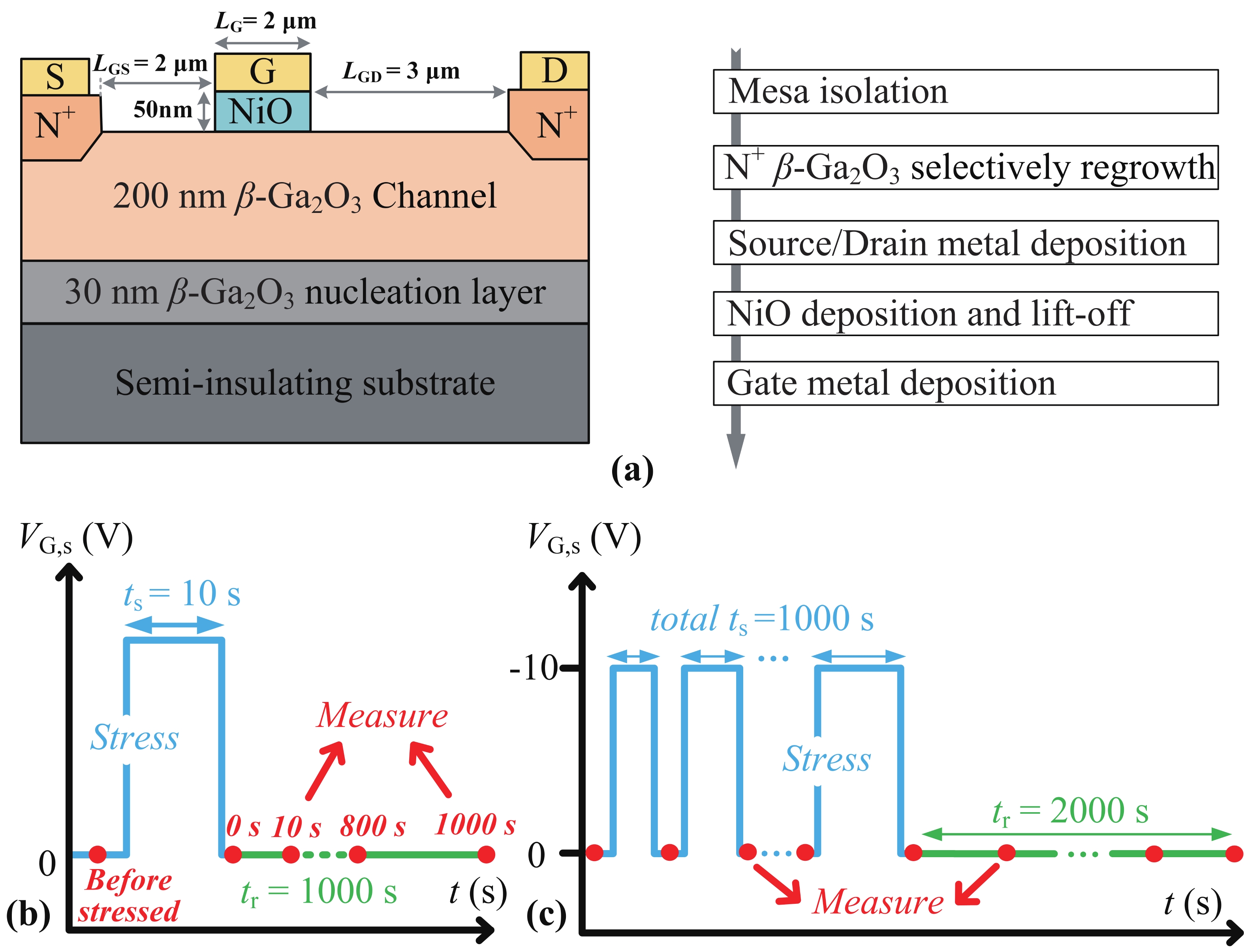
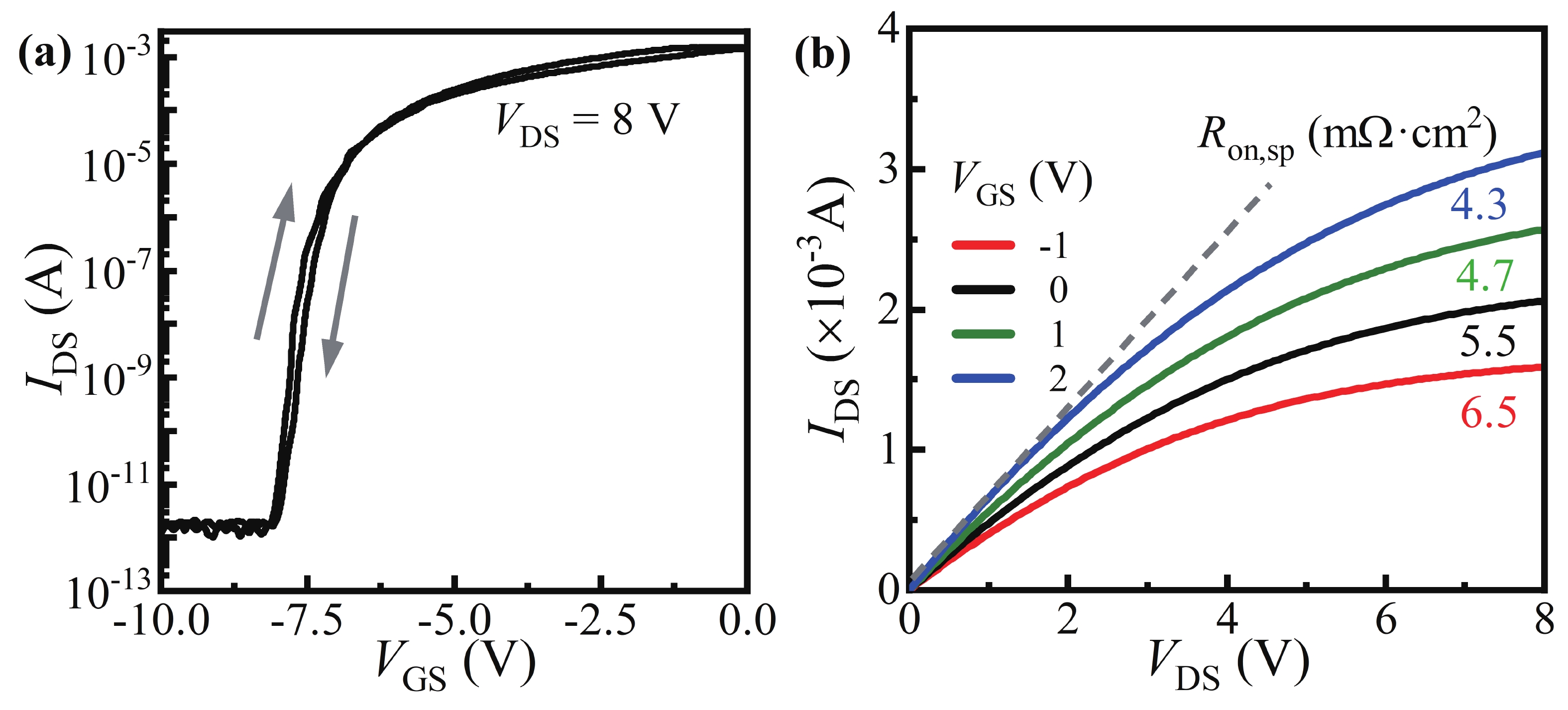
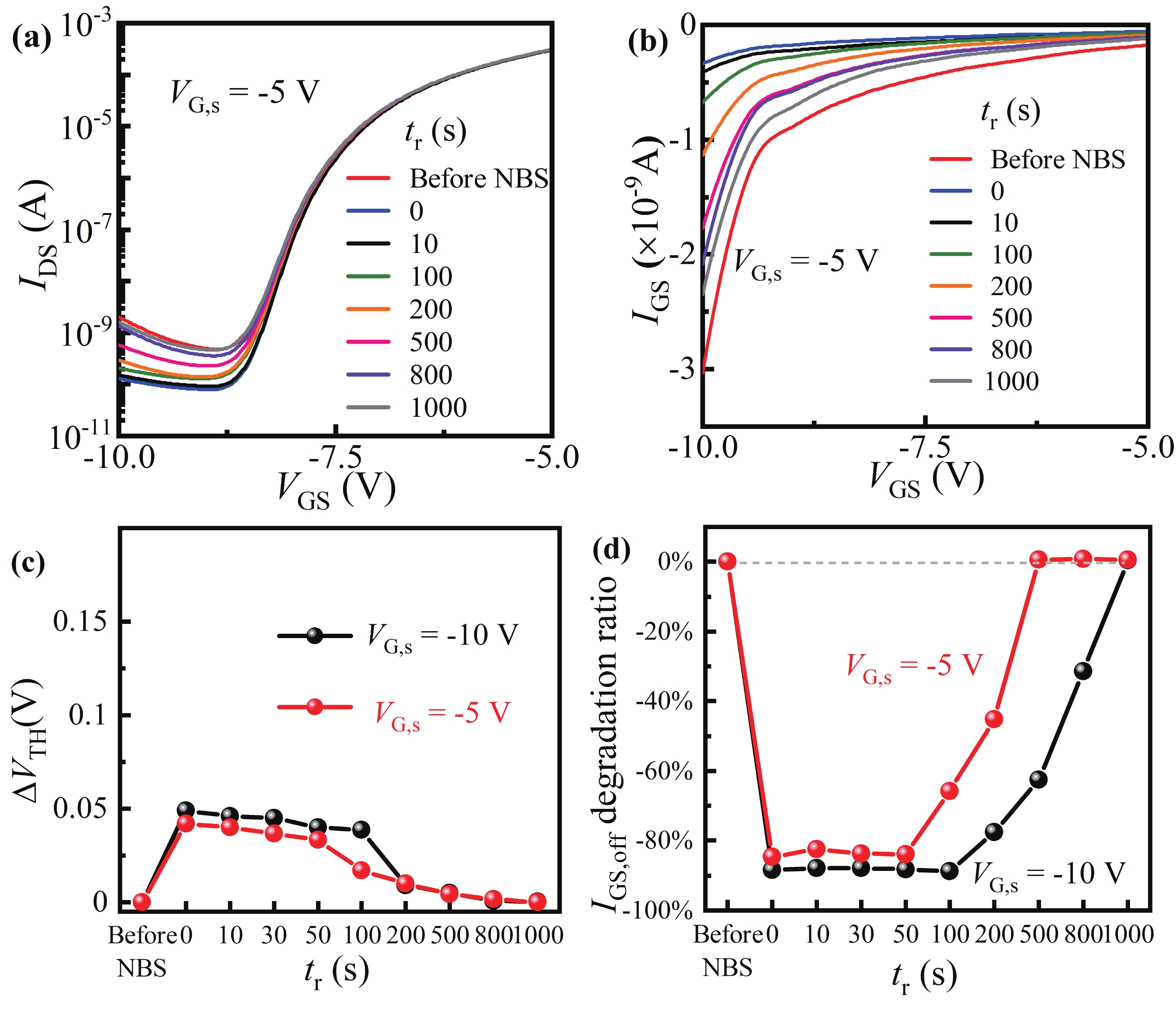
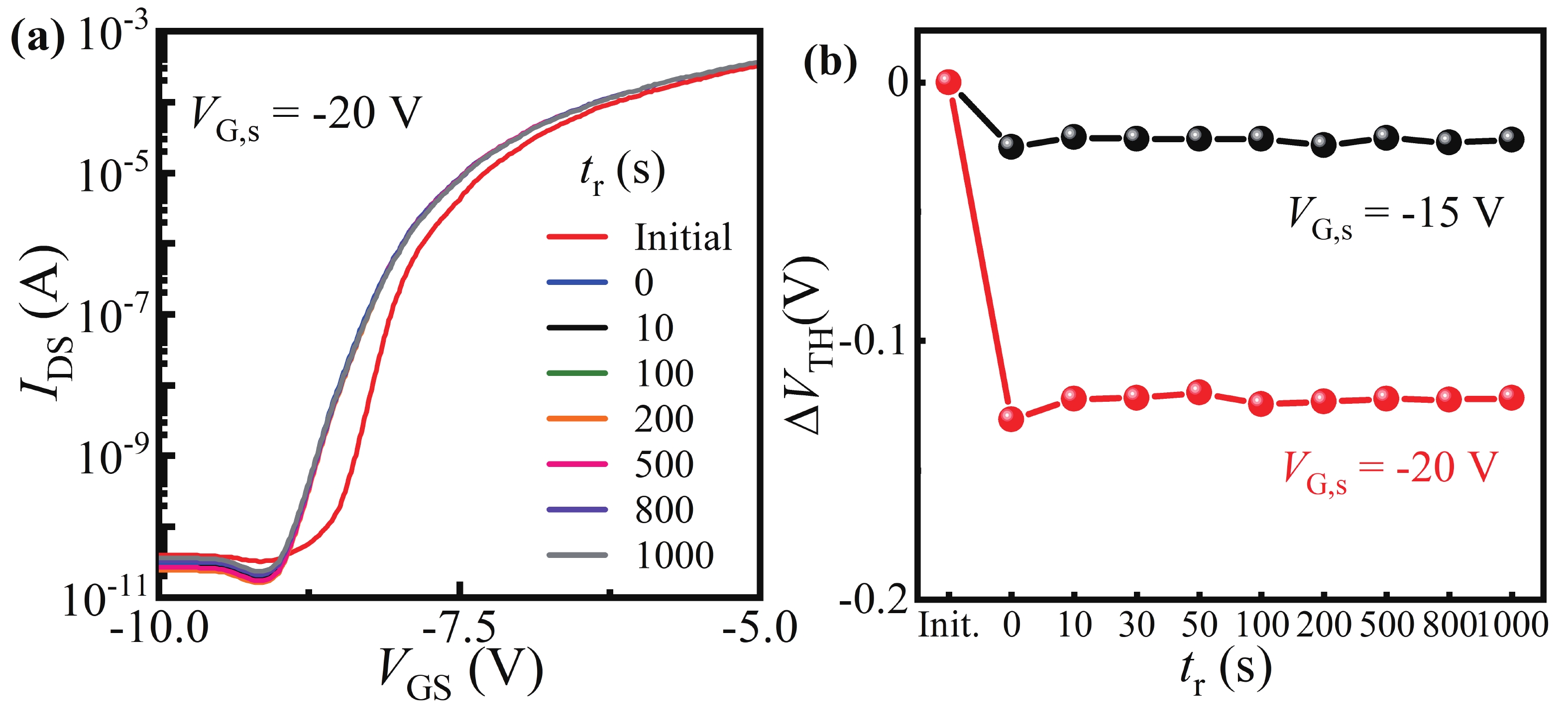
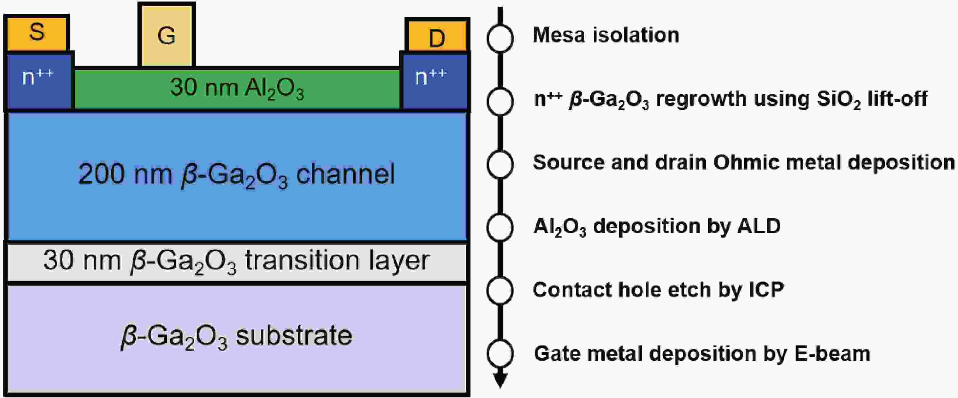
A NiO/β-Ga2O3 heterojunction-gate field effect transistor (HJ-FET) is fabricated and its instability mechanisms are experimentally investigated under different gate stress voltage (VG,s) and stress times (ts). Two different degradation mechanisms of the devices under negative bias stress (NBS) are identified. At low VG,s for a short ts, NiO bulk traps trapping/de-trapping electrons are responsible for decrease/recovery of the leakage current, respectively. At higher VG,s or long ts, the device transfer characteristic curves and threshold voltage (VTH) are almost permanently negatively shifted. This is because the interface dipoles are almost permanently ionized and neutralize the ionized charges in the space charge region (SCR) across the heterojunction interface, resulting in a narrowing SCR. This provides an important theoretical guide to study the reliability of NiO/β-Ga2O3 heterojunction devices in power electronic applications.


J. Semicond.
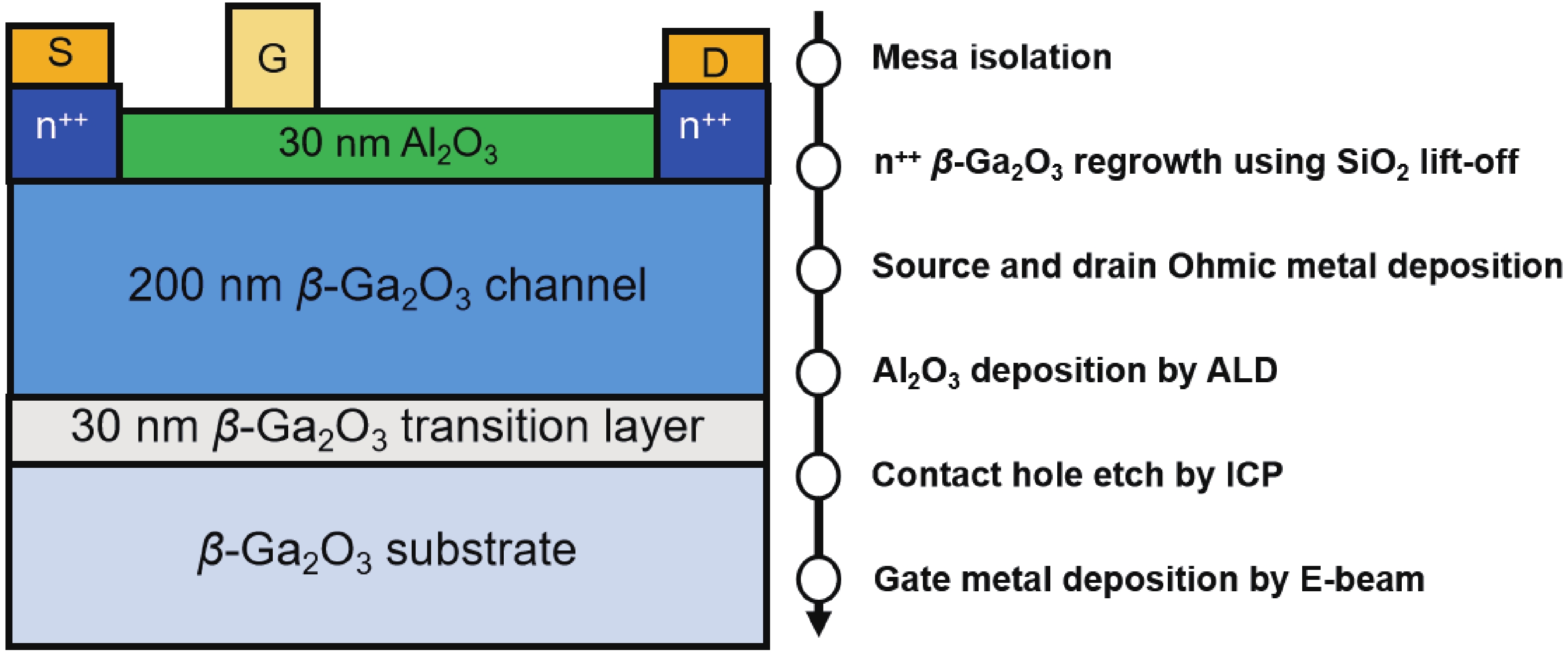
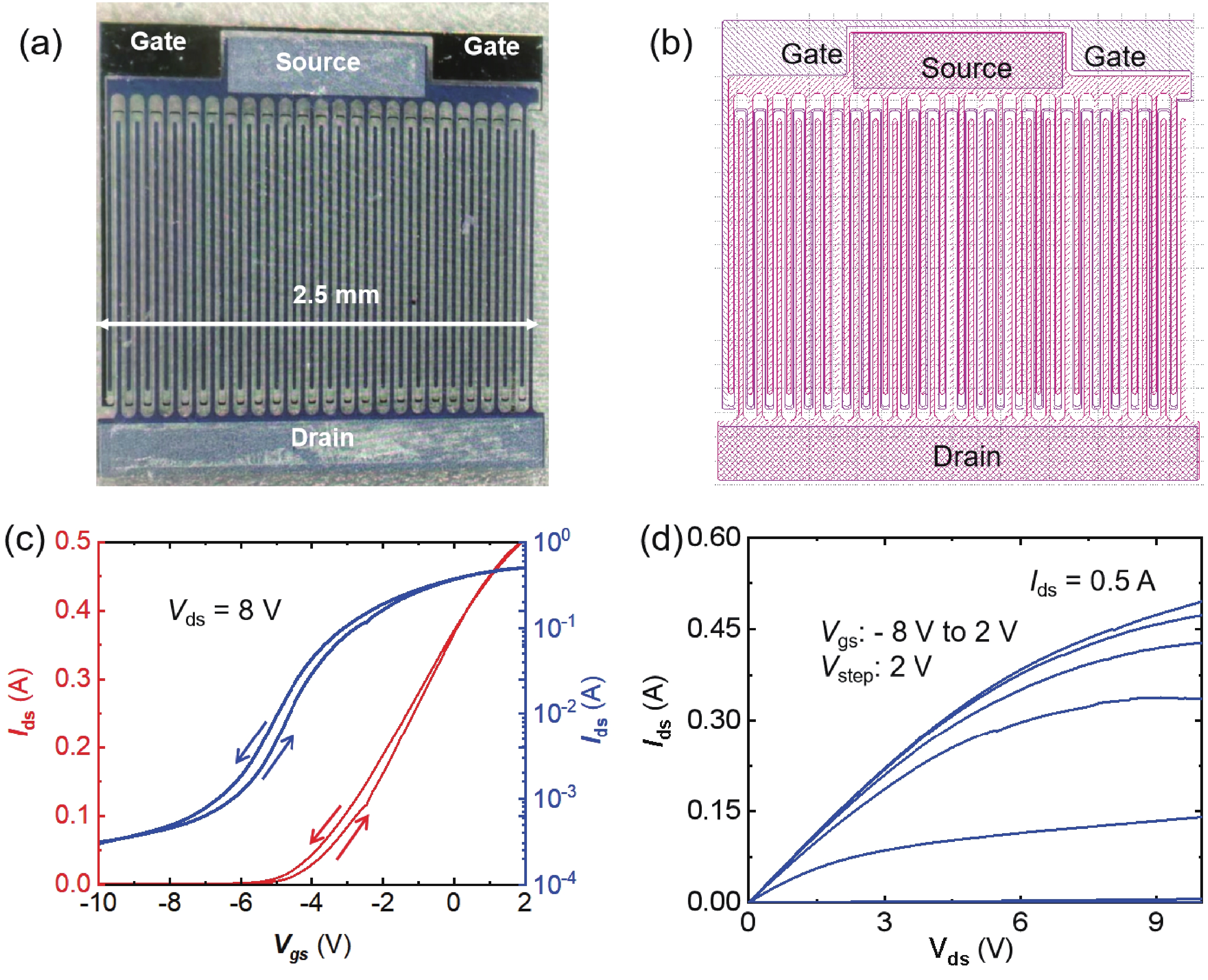
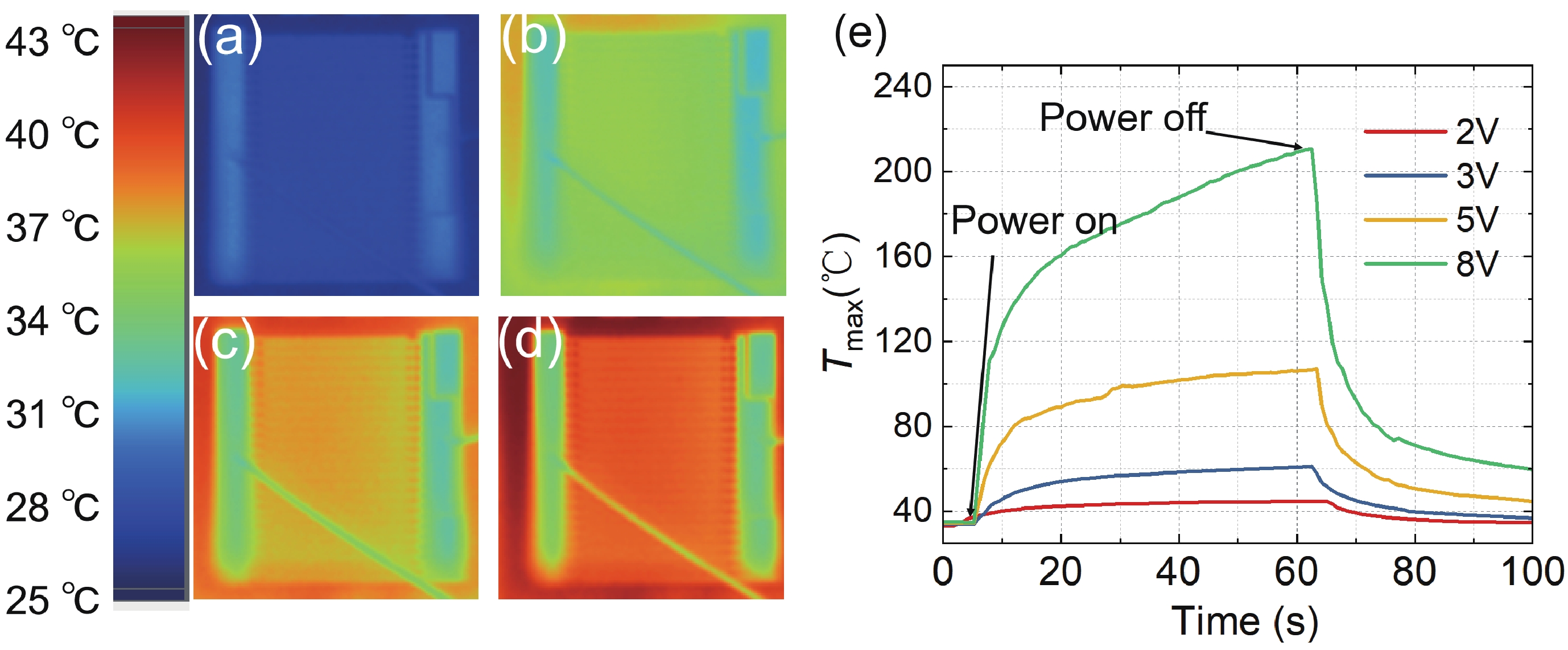
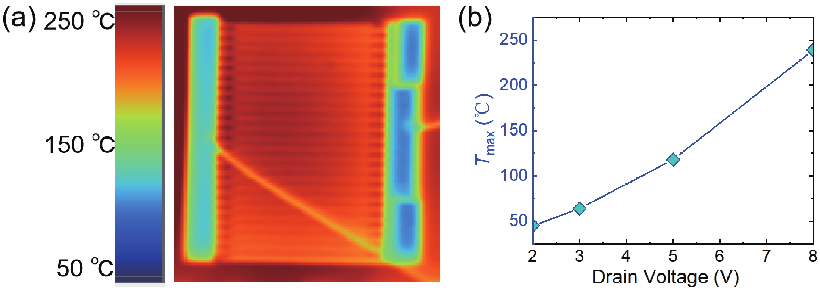
2023, 44(7): 072804 doi: 10.1088/1674-4926/44/7/072804
The self-heating effect severely limits device performance and reliability. Although some studies have revealed the heat distribution of β-Ga2O3 MOSFETs under biases, those devices all have small areas and have difficulty reflecting practical conditions. This work demonstrated a multi-finger β-Ga2O3 MOSFET with a maximum drain current of 0.5 A. Electrical characteristics were measured, and the heat dissipation of the device was investigated through infrared images. The relationship between device temperature and time/bias is analyzed.

J. Semicond.
2023, 44(7): 072805 doi: 10.1088/1674-4926/44/7/072805
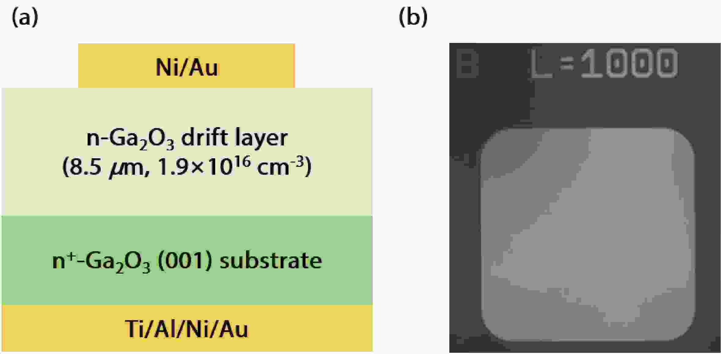
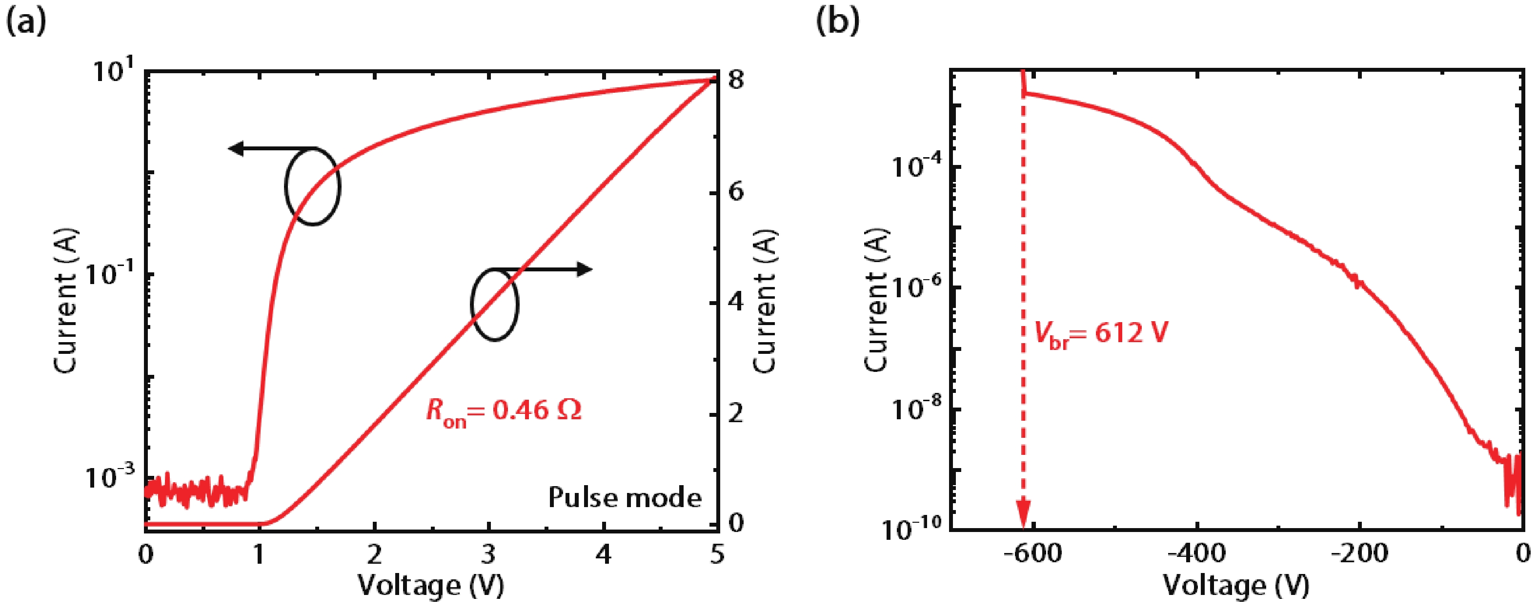
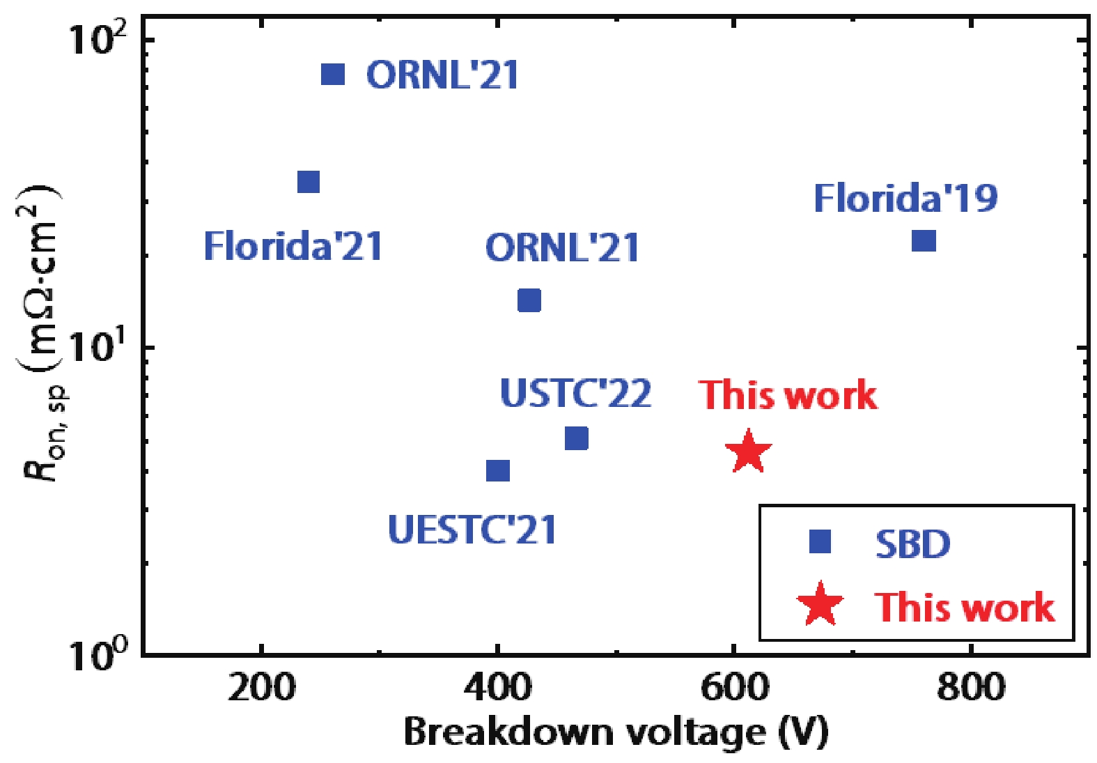
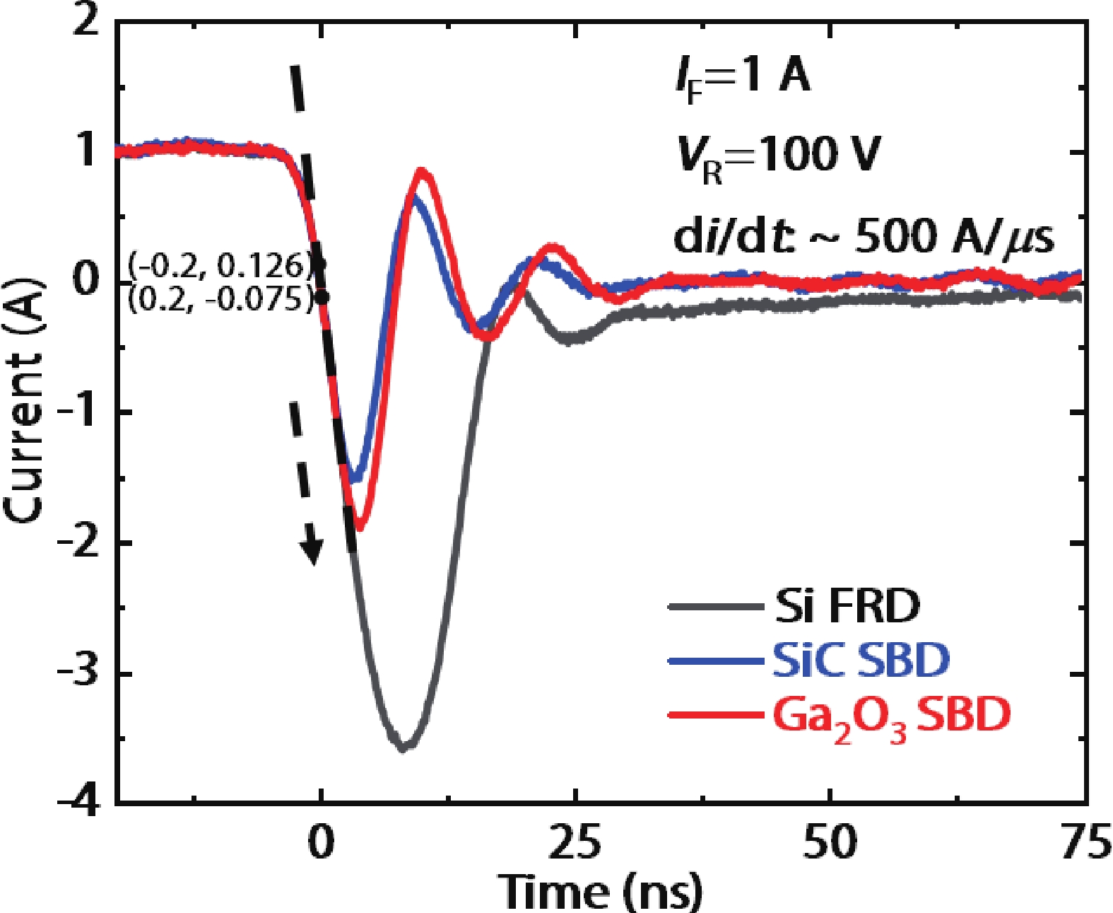
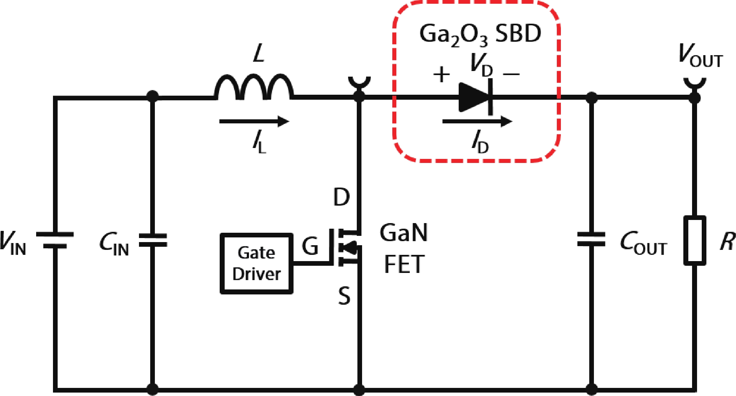
We demonstrate superb large-area vertical β-Ga2O3 SBDs with a Schottky contact area of 1 × 1 mm2 and obtain a high-efficiency DC–DC converter based on the device. The β-Ga2O3 SBD can obtain a forward current of 8 A with a forward voltage of 5 V, and has a reverse breakdown voltage of 612 V. The forward turn-on voltage (VF) and the on-resistance (Ron) are 1.17 V and 0.46 Ω, respectively. The conversion efficiency of the β-Ga2O3 SBD-based DC–DC converter is 95.81%. This work indicates the great potential of Ga2O3 SBDs and relevant circuits in power electronic applications.


J. Semicond.
2023, 44(7): 072806 doi: 10.1088/1674-4926/44/7/072806
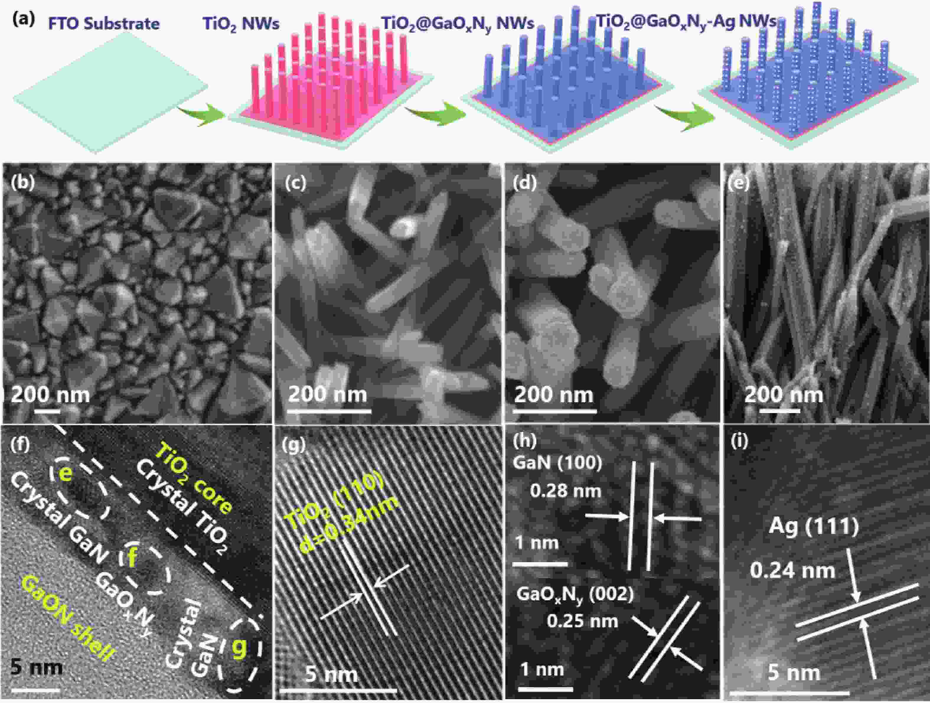
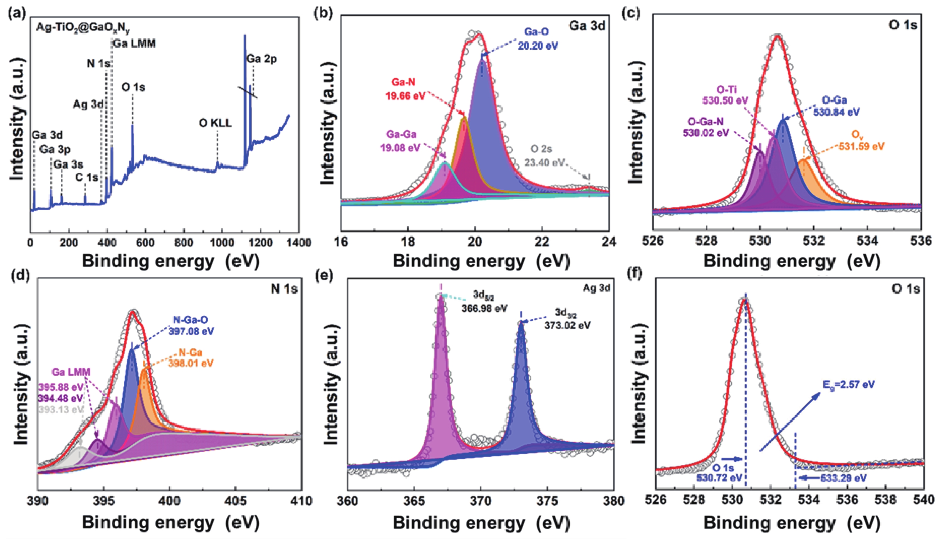
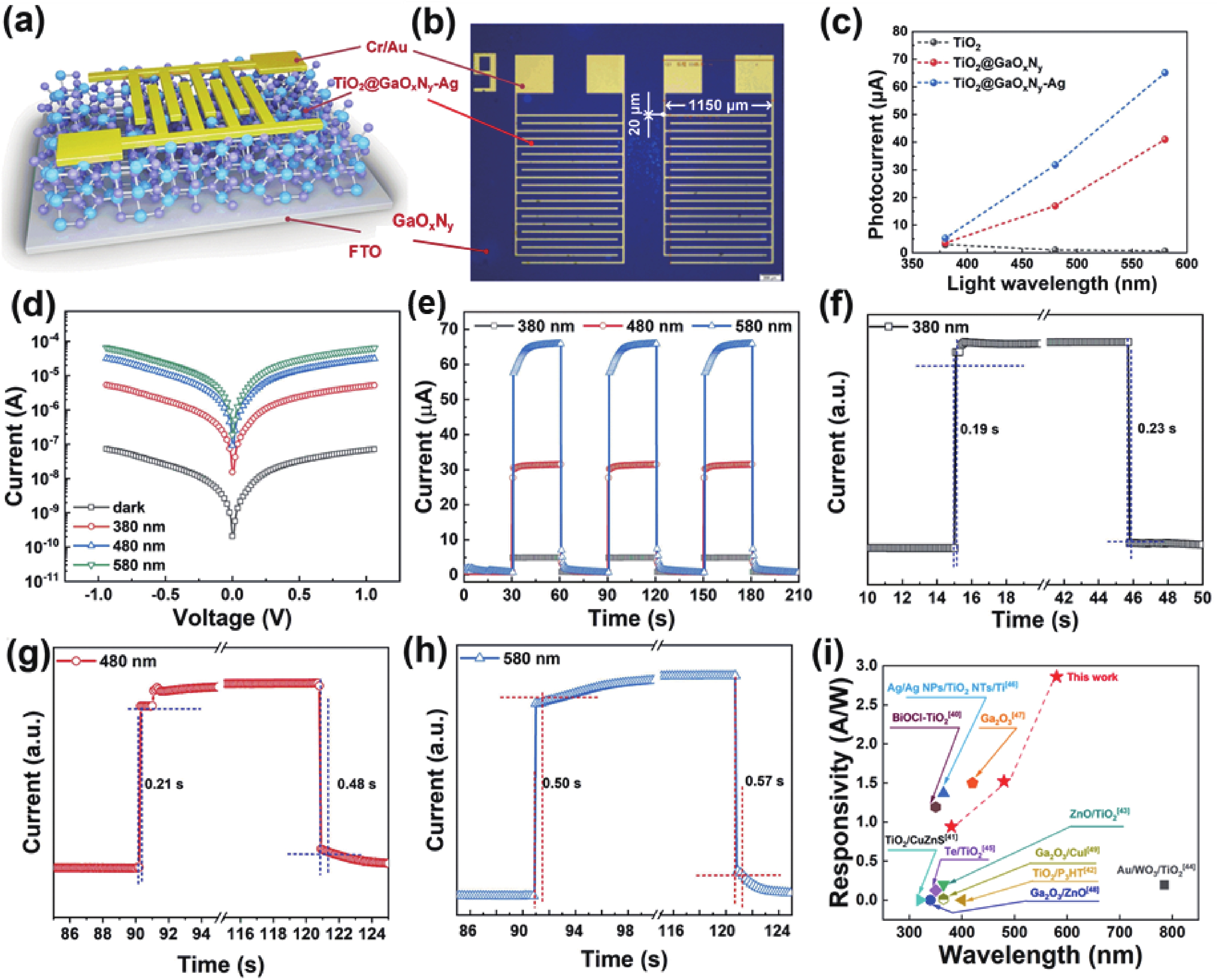
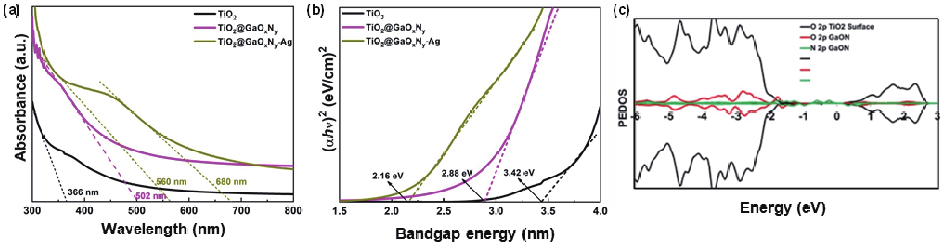
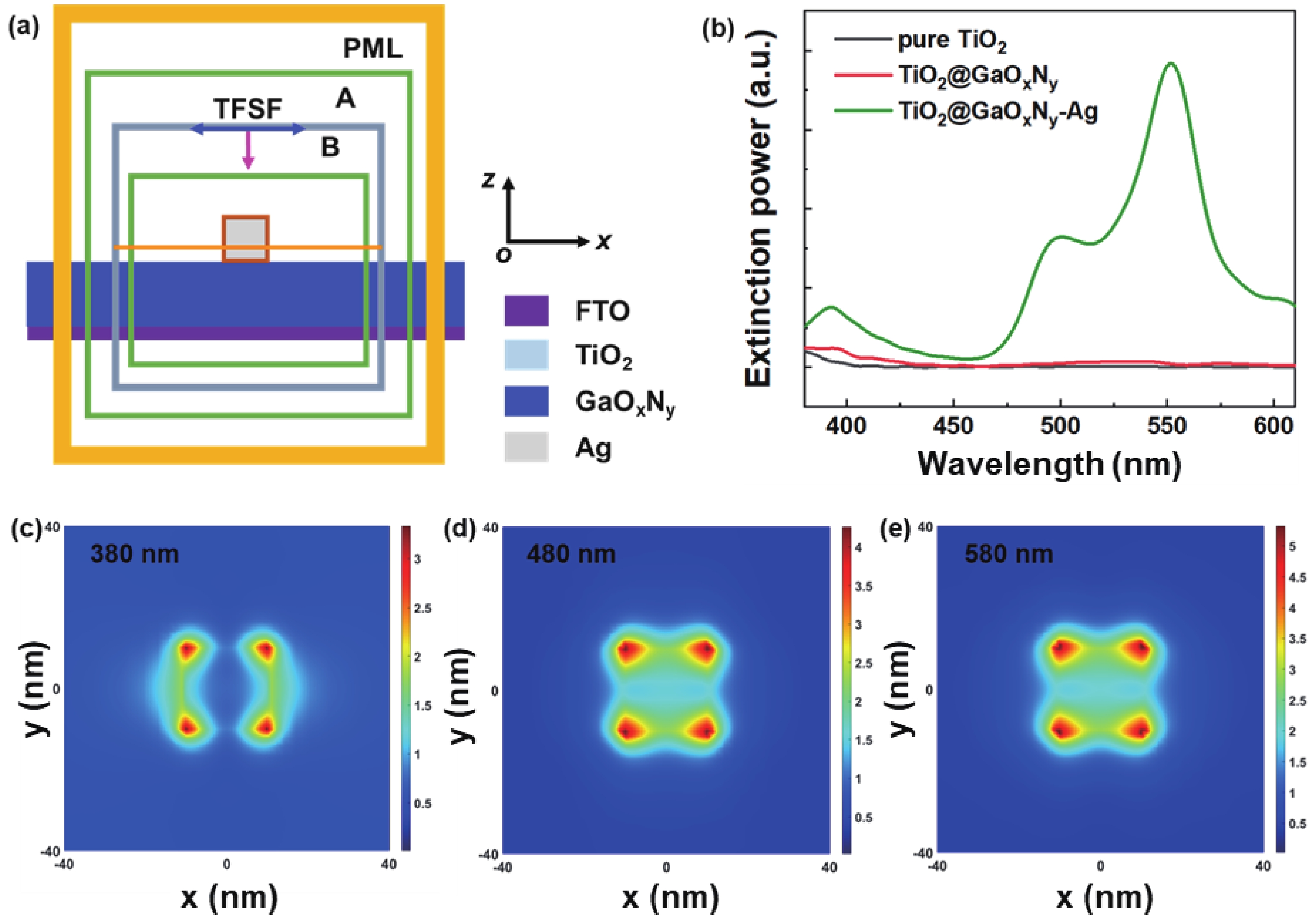
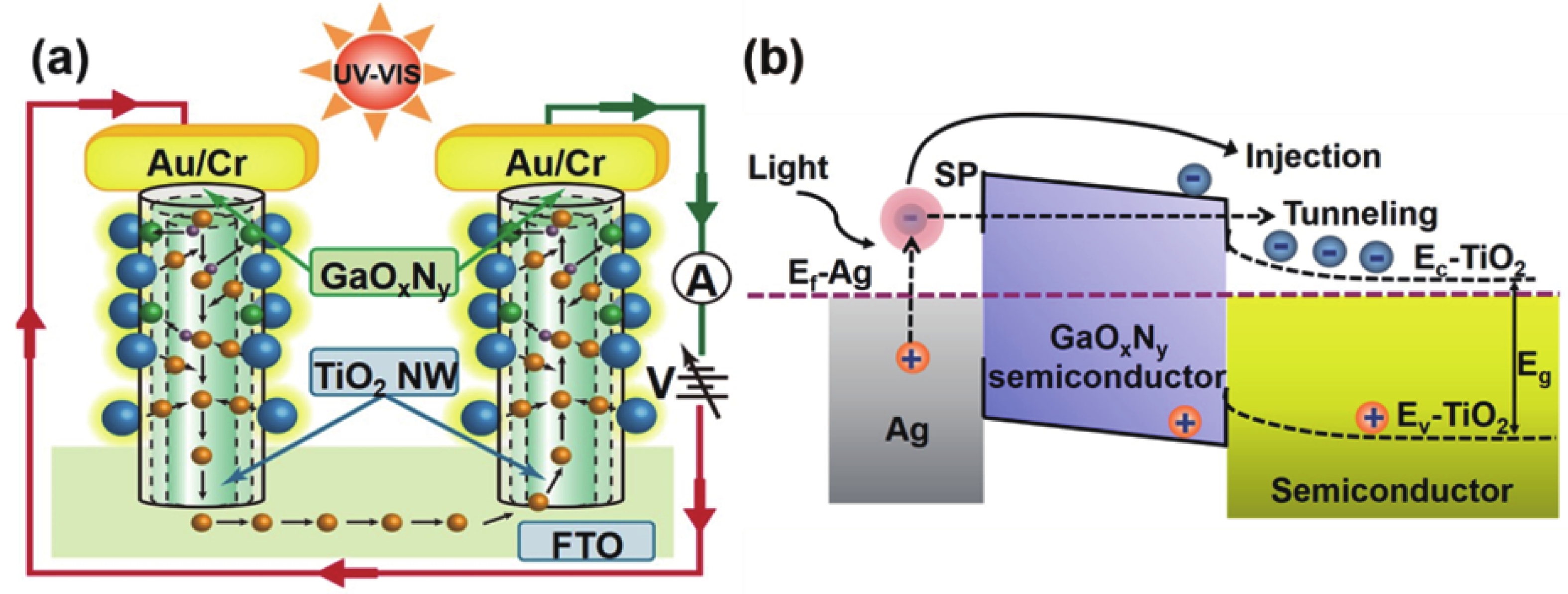
In this work, we reported a high-performance-based ultraviolet-visible (UV-VIS) photodetector based on a TiO2@GaOxNy-Ag heterostructure. Ag particles were introduced into TiO2@GaOxNy to enhance the visible light detection performance of the heterojunction device. At 380 nm, the responsivity and detectivity of TiO2@GaOxNy-Ag were 0.94 A/W and 4.79 × 10⁹ Jones, respectively, and they increased to 2.86 A/W and 7.96 × 10¹⁰ Jones at 580 nm. The rise and fall times of the response were 0.19/0.23 and 0.50/0.57 s, respectively. Uniquely, at 580 nm, the responsivity of fabricated devices is one to four orders of magnitude higher than that of the photodetectors based on TiO2, Ga2O3, and other heterojunctions. The excellent optoelectronic characteristics of the TiO2@GaOxNy-Ag heterojunction device could be mainly attributed to the synergistic effect of the type-Ⅱ band structure of the metal–semiconductor–metal heterojunction and the plasmon resonance effect of Ag, which not only effectively promotes the separation of photogenerated carriers but also reduces the recombination rate. It is further illuminated by finite difference time domain method (FDTD) simulation and photoelectric measurements. The TiO2@GaOxNy-Ag arrays with high-efficiency detection are suitable candidates for applications in energy-saving communication, imaging, and sensing networks.
J. Semicond.
2023, 44(7): 072807 doi: 10.1088/1674-4926/44/7/072807
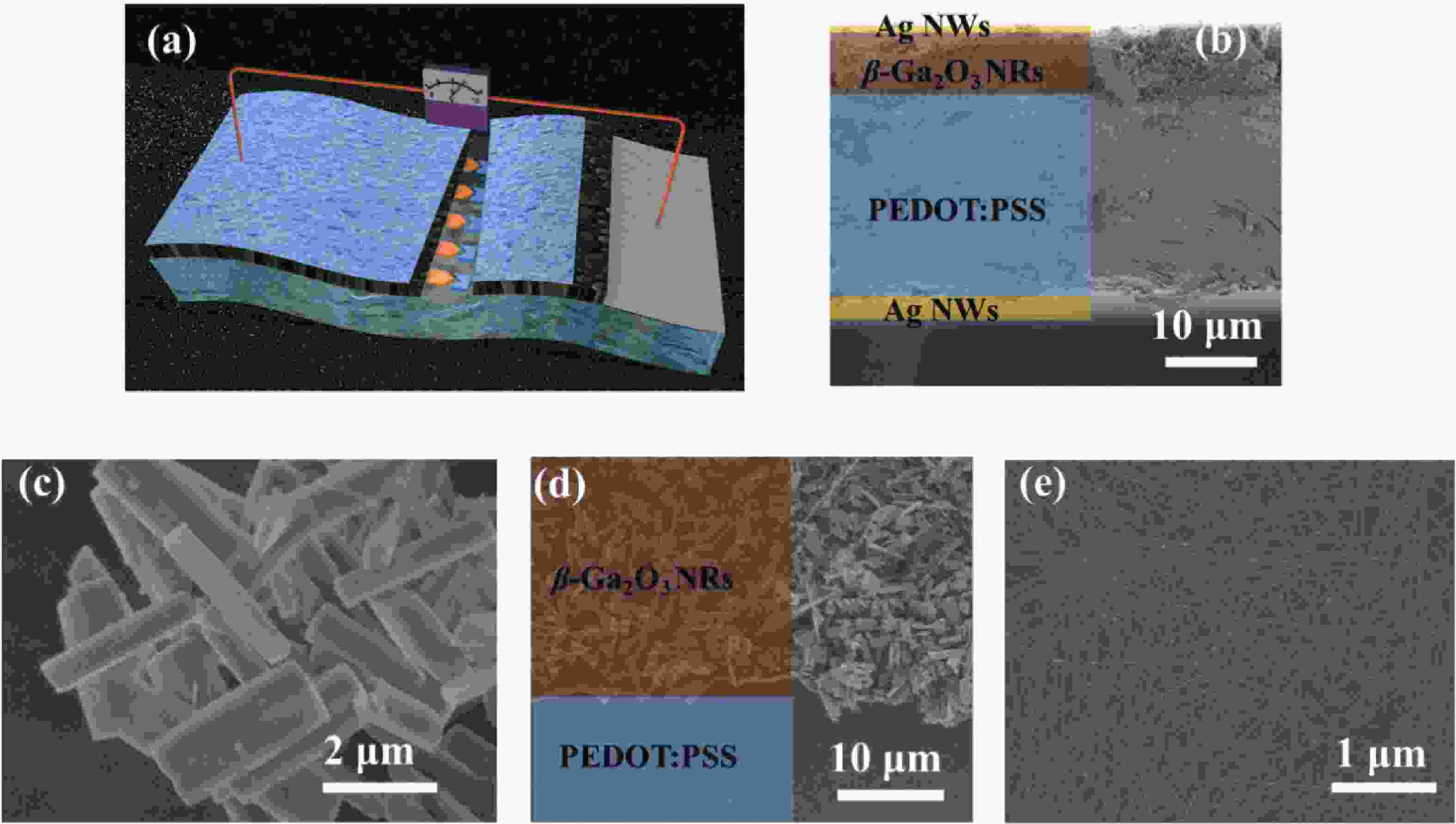
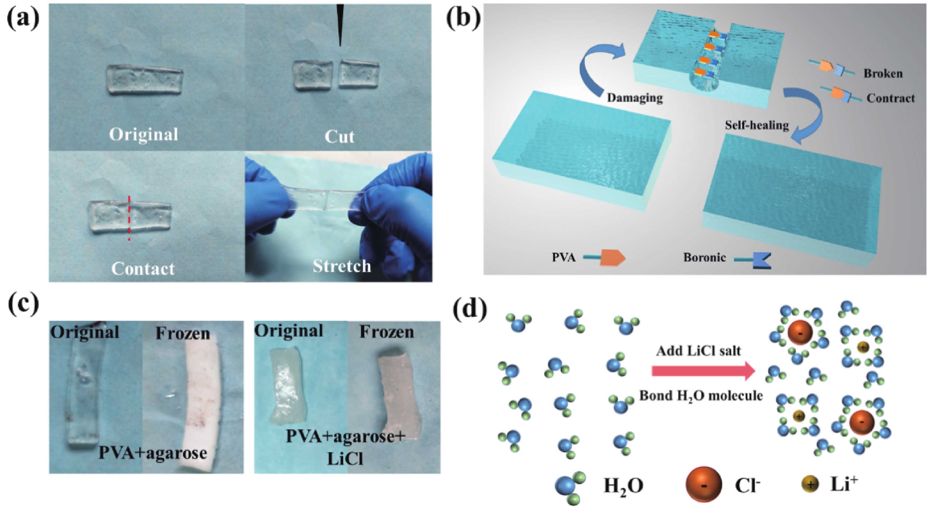
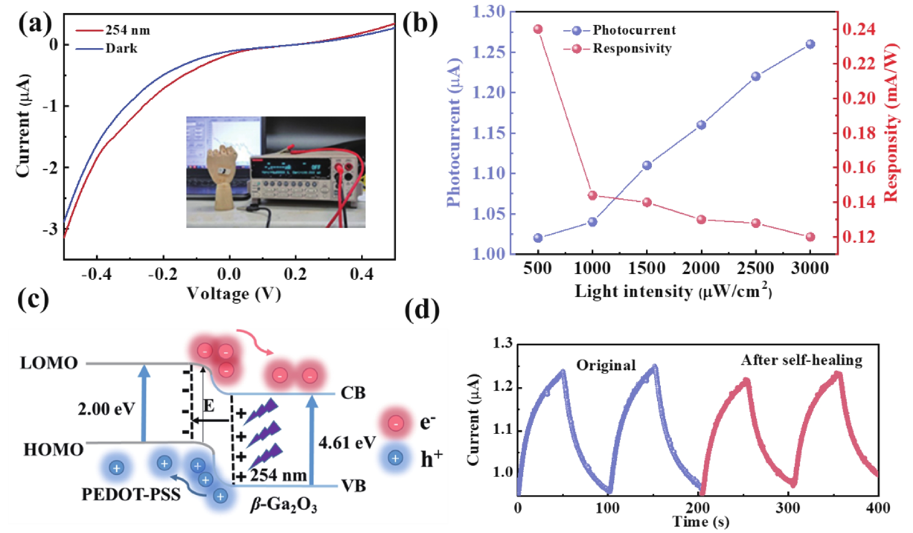
Gallium oxide (Ga2O3) based flexible heterojunction type deep ultraviolet (UV) photodetectors show excellent solar-blind photoelectric performance, even when not powered, which makes them ideal for use in intelligent wearable devices. However, traditional flexible photodetectors are prone to damage during use due to poor toughness, which reduces the service life of these devices. Self-healing hydrogels have been demonstrated to have the ability to repair damage and their combination with Ga2O3 could potentially improve the lifetime of the flexible photodetectors while maintaining their performance. Herein, a novel self-healing and self-powered flexible photodetector has been constructed onto the hydrogel substrate, which exhibits an excellent responsivity of 0.24 mA/W under 254 nm UV light at zero bias due to the built-in electric field originating from the PEDOT: PSS/Ga2O3 heterojunction. The self-healing of the Ga2O3 based photodetector was enabled by the reversible property of the synthesis of agarose and polyvinyl alcohol double network, which allows the photodetector to recover its original configuration and function after damage. After self-healing, the photocurrent of the photodetector decreases from 1.23 to 1.21 μA, while the dark current rises from 0.95 to 0.97 μA, with a barely unchanged of photoresponse speed. Such a remarkable recovery capability and the photodetector’s superior photoelectric performance not only significantly enhance a device lifespan but also present new possibilities to develop wearable and intelligent electronics in the future.


J. Semicond.
2023, 44(7): 074101 doi: 10.1088/1674-4926/44/7/074101
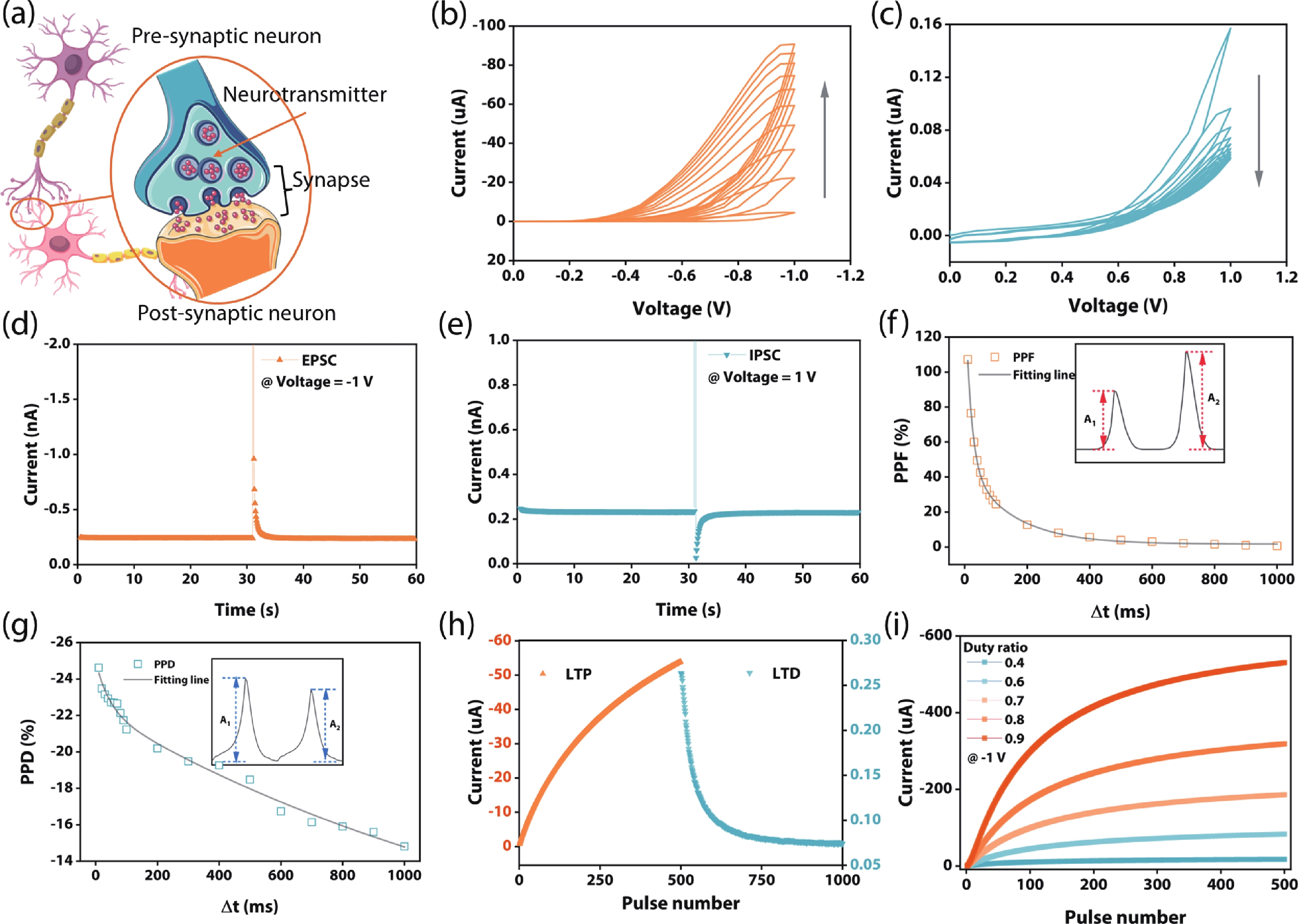
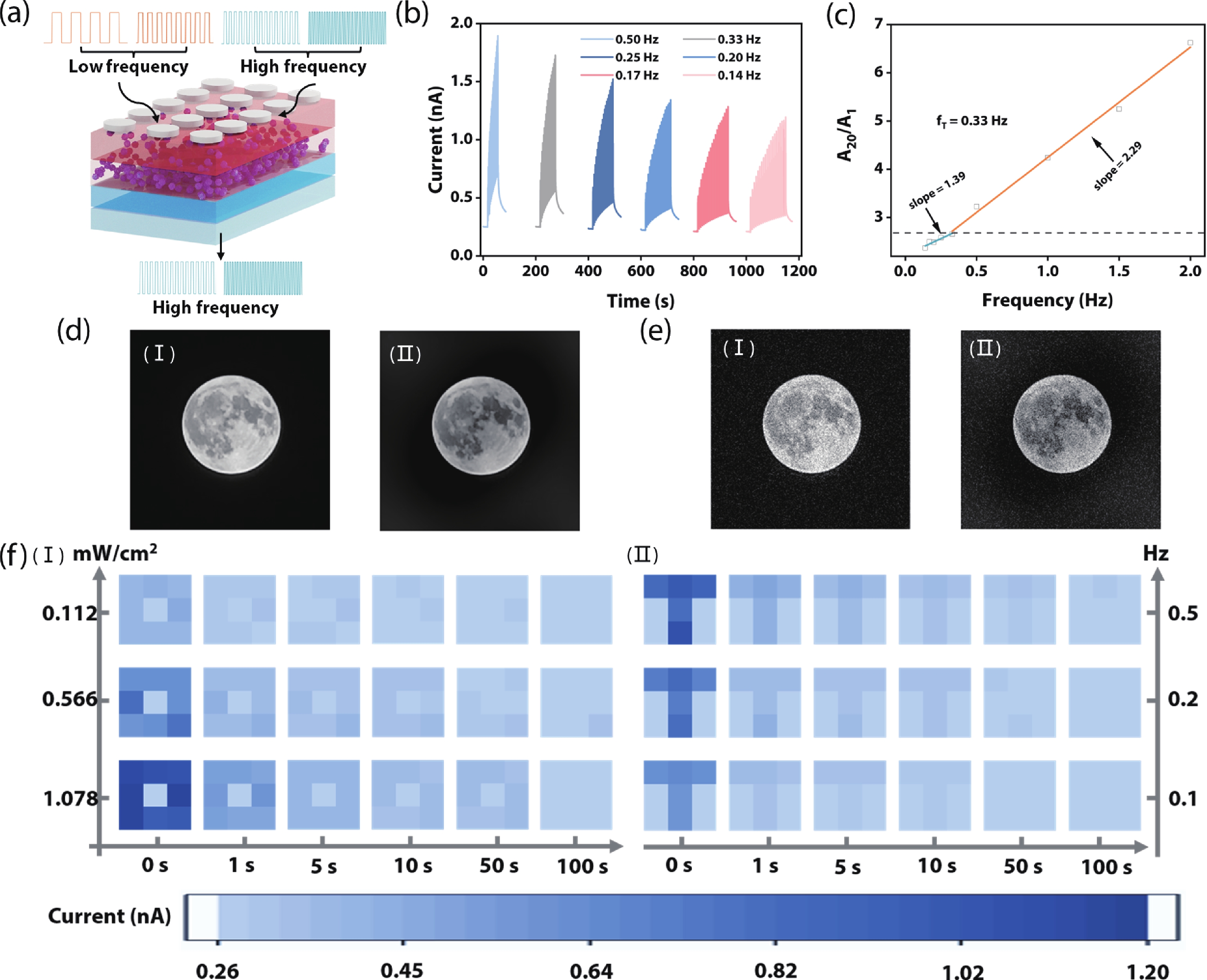
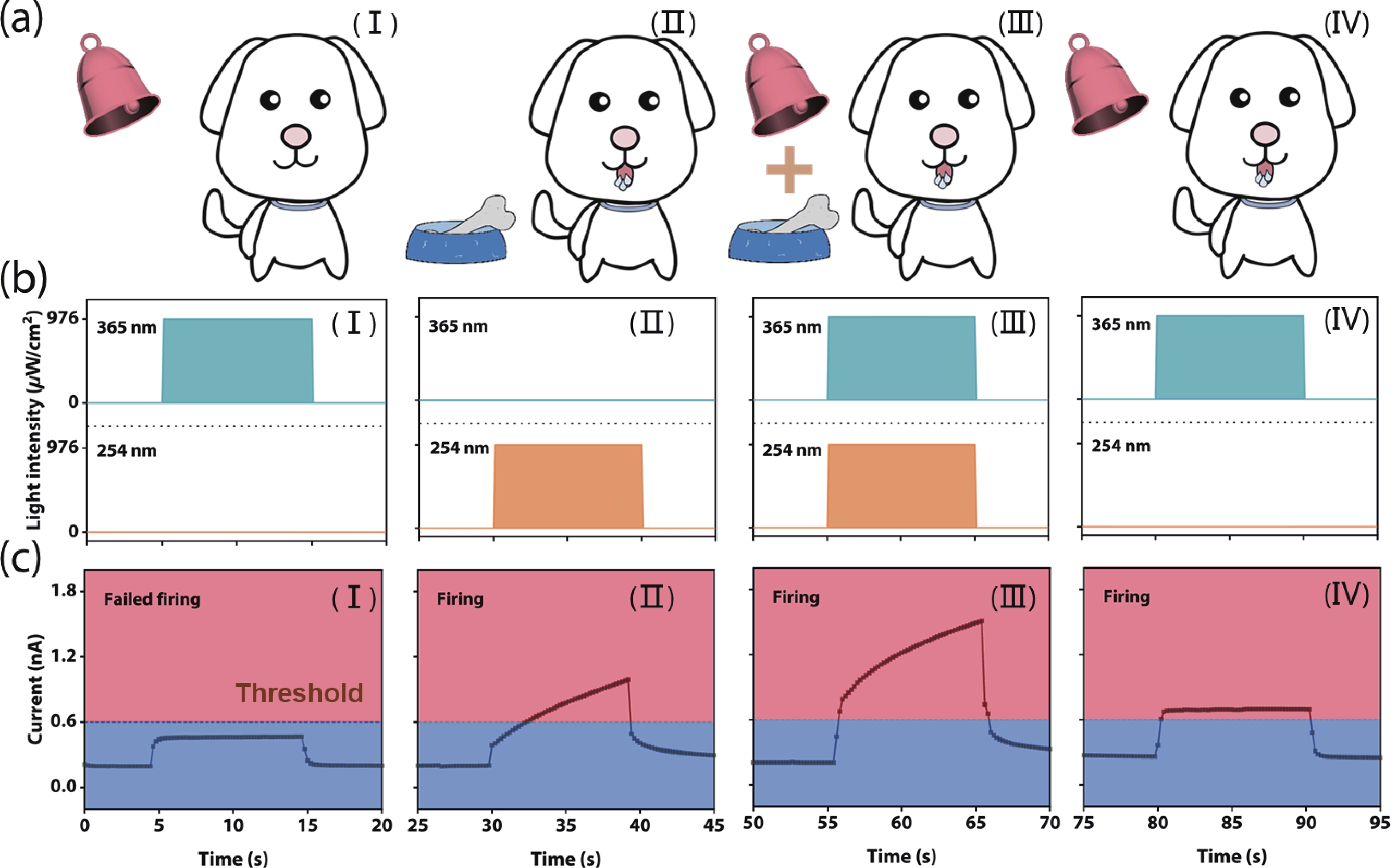
In the era of accelerated development in artificial intelligence as well as explosive growth of information and data throughput, underlying hardware devices that can integrate perception and memory while simultaneously offering the benefits of low power consumption and high transmission rates are particularly valuable. Neuromorphic devices inspired by the human brain are considered to be one of the most promising successors to the efficient in-sensory process. In this paper, a homojunction-based multi-functional optoelectronic synapse (MFOS) is proposed and testified. It enables a series of basic electrical synaptic plasticity, including paired-pulse facilitation/depression (PPF/PPD) and long-term promotion/depression (LTP/LTD). In addition, the synaptic behaviors induced by electrical signals could be instead achieved through optical signals, where its sensitivity to optical frequency allows the MFOS to simulate high-pass filtering applications in situ and the perception capability integrated into memory endows it with the information acquisition and processing functions as a visual system. Meanwhile, the MFOS exhibits its performances of associative learning and logic gates following the illumination with two different wavelengths. As a result, the proposed MFOS offers a solution for the realization of intelligent visual system and bionic electronic eye, and will provide more diverse application scenarios for future neuromorphic computing.