Issue Browser
Volume 44, Issue 8,
Aug 2023


J. Semicond.
2023, 44(8): 081701 doi: 10.1088/1674-4926/44/8/081701

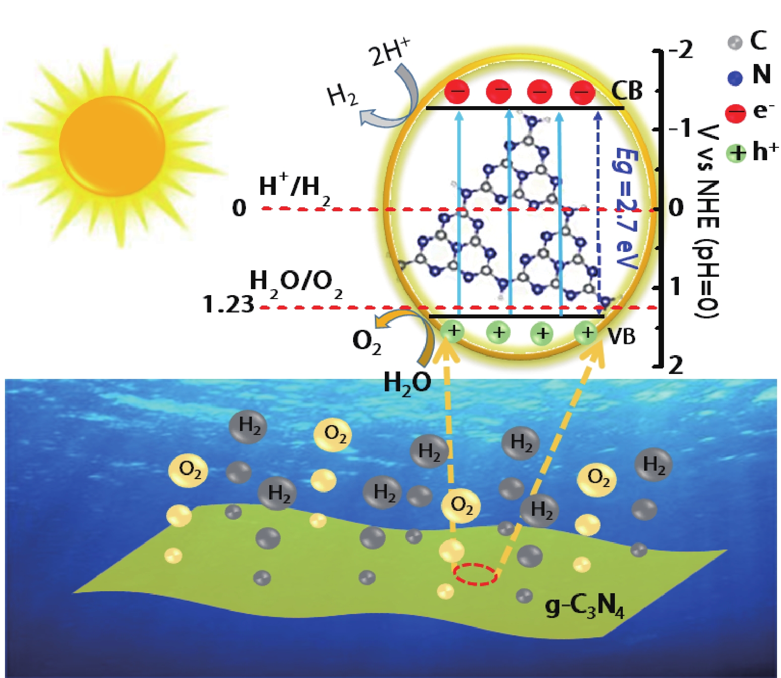
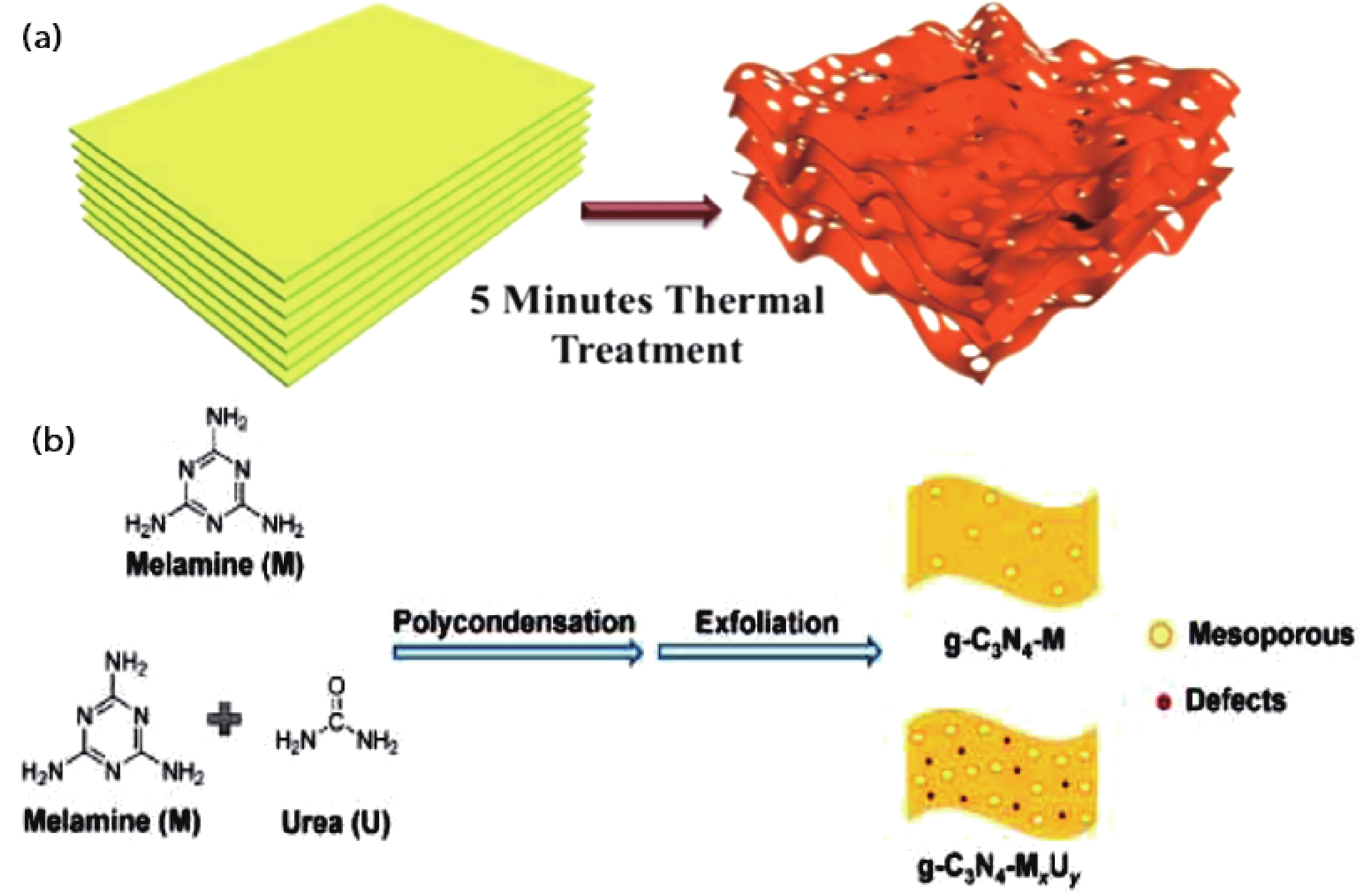
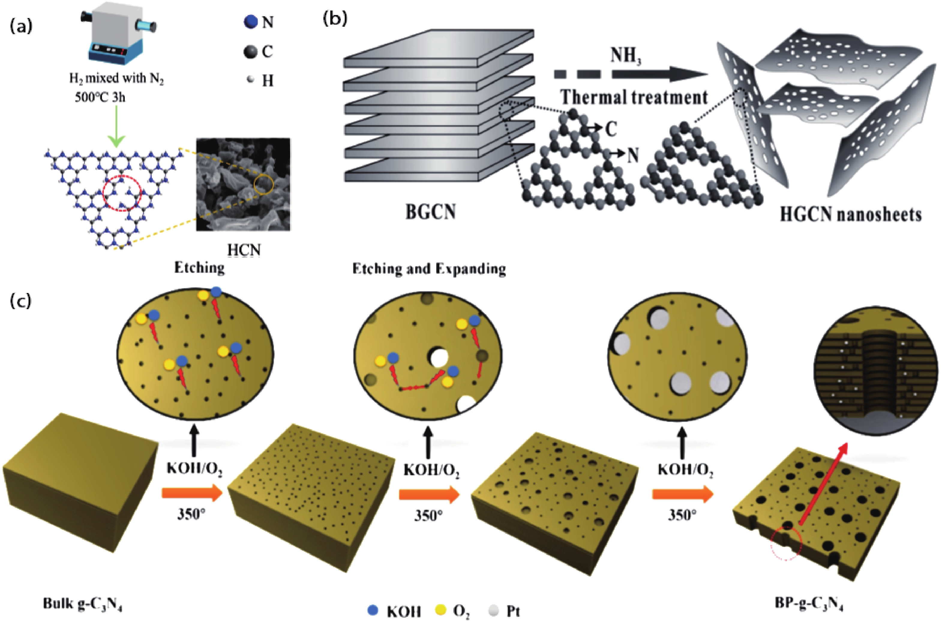
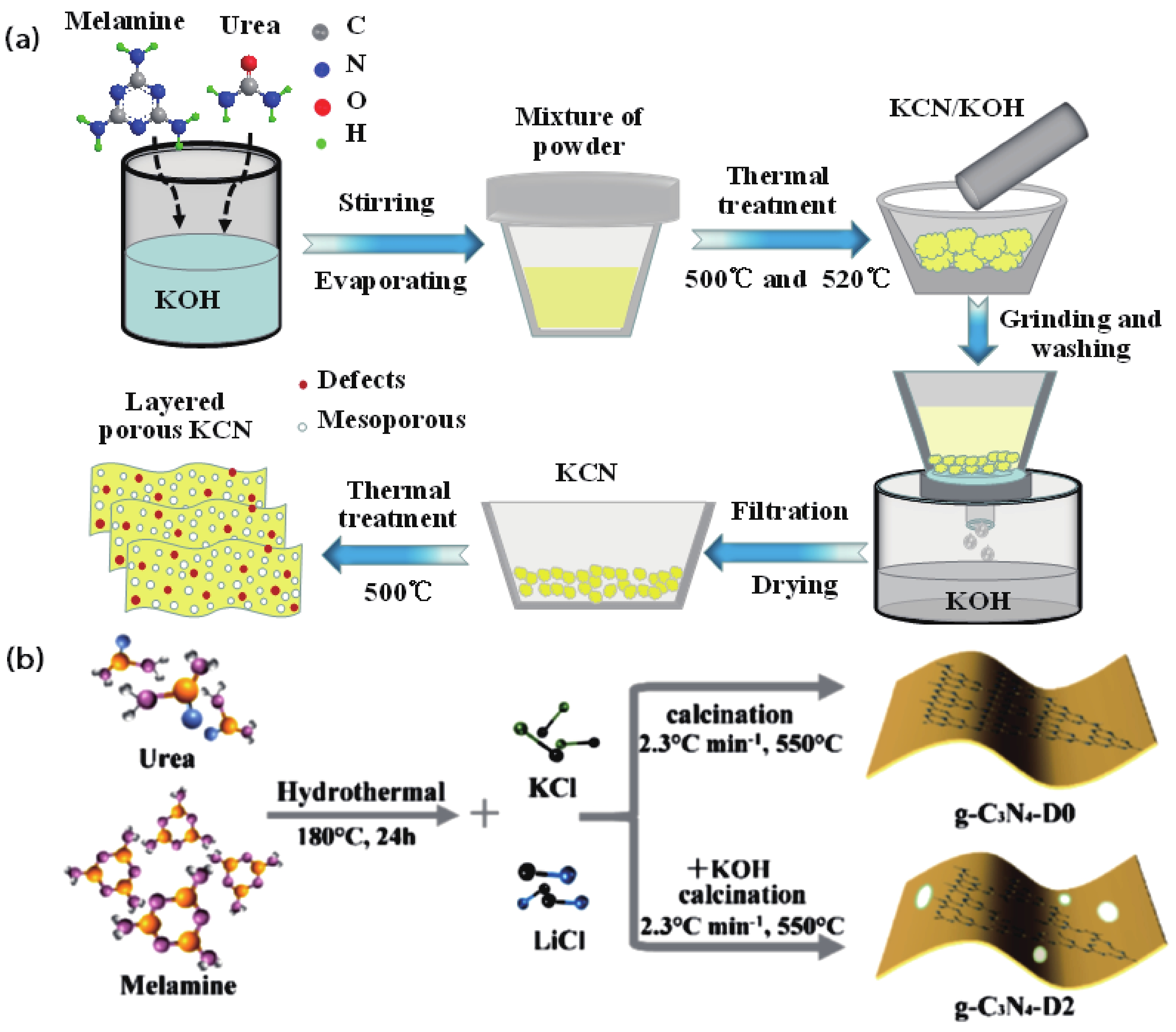
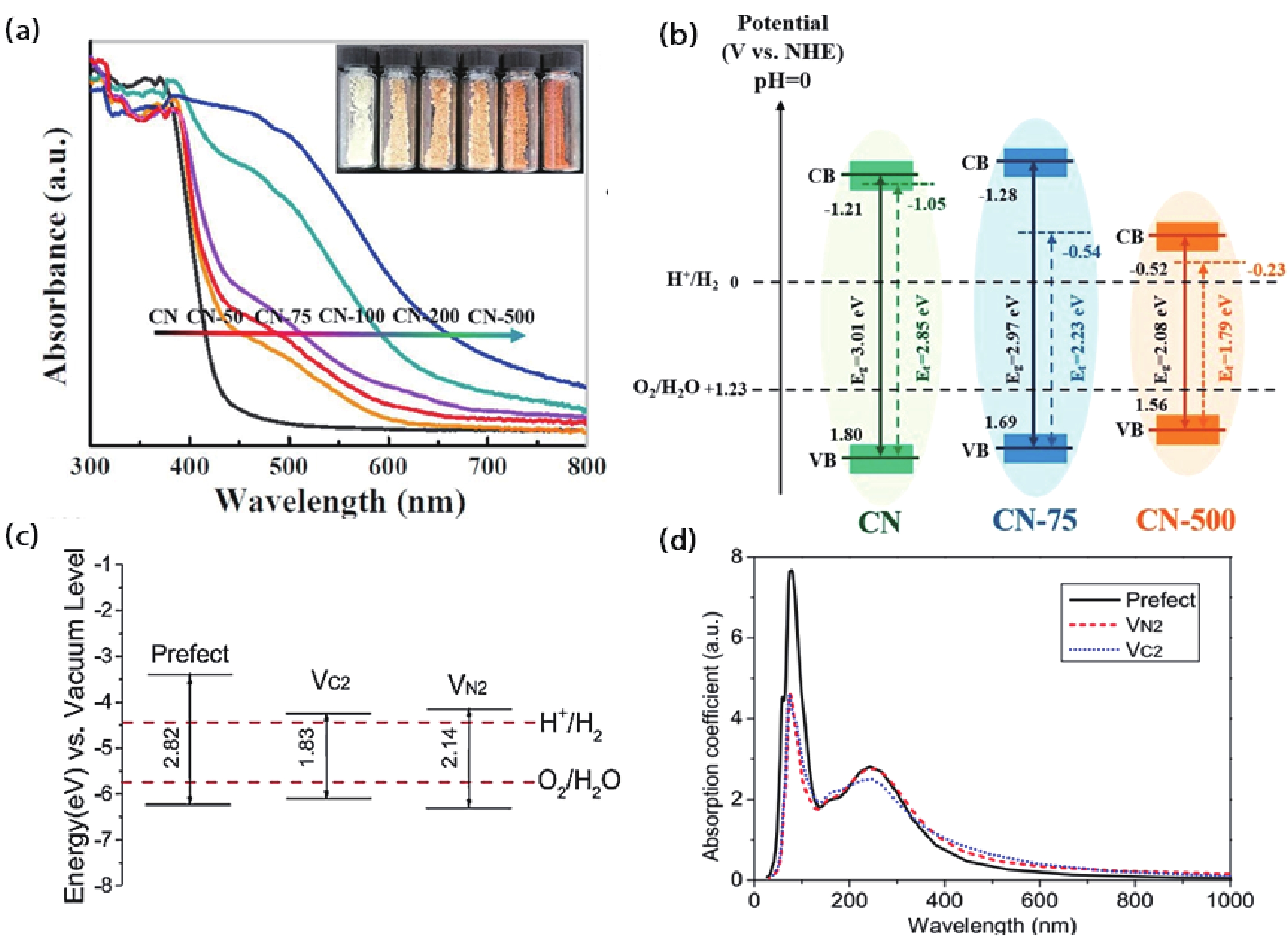
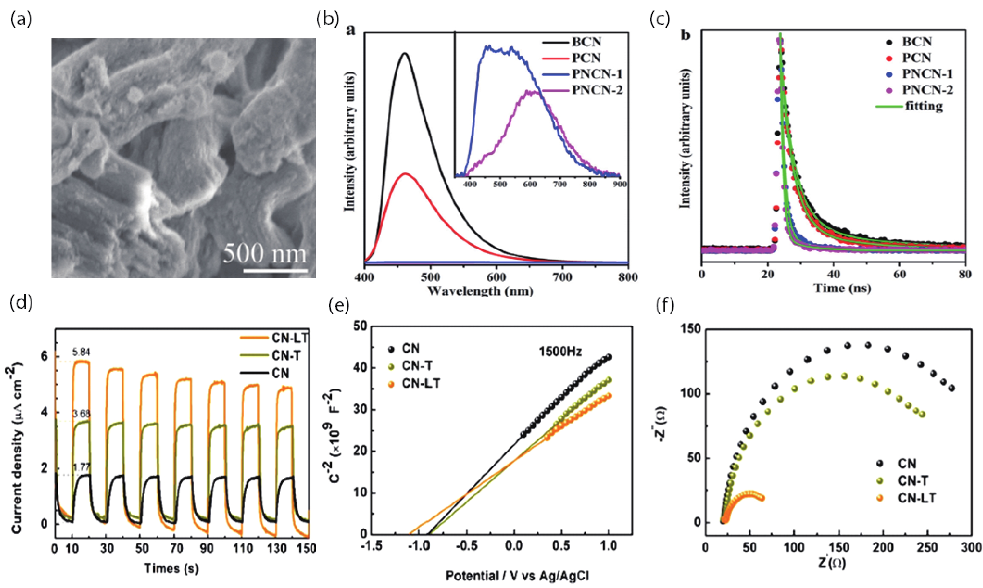
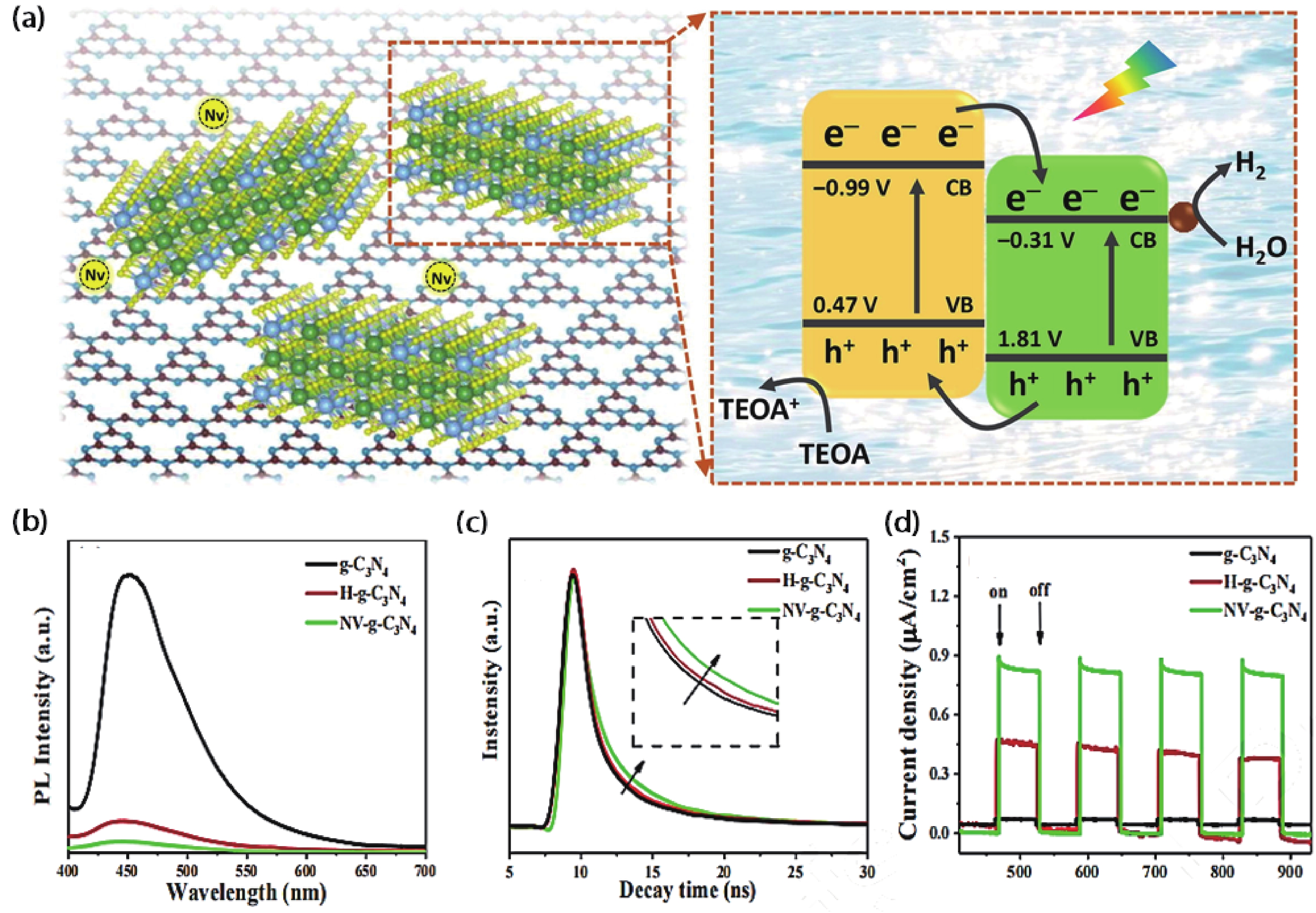
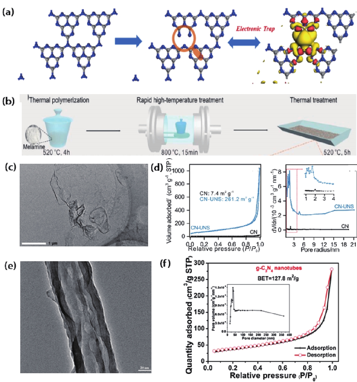
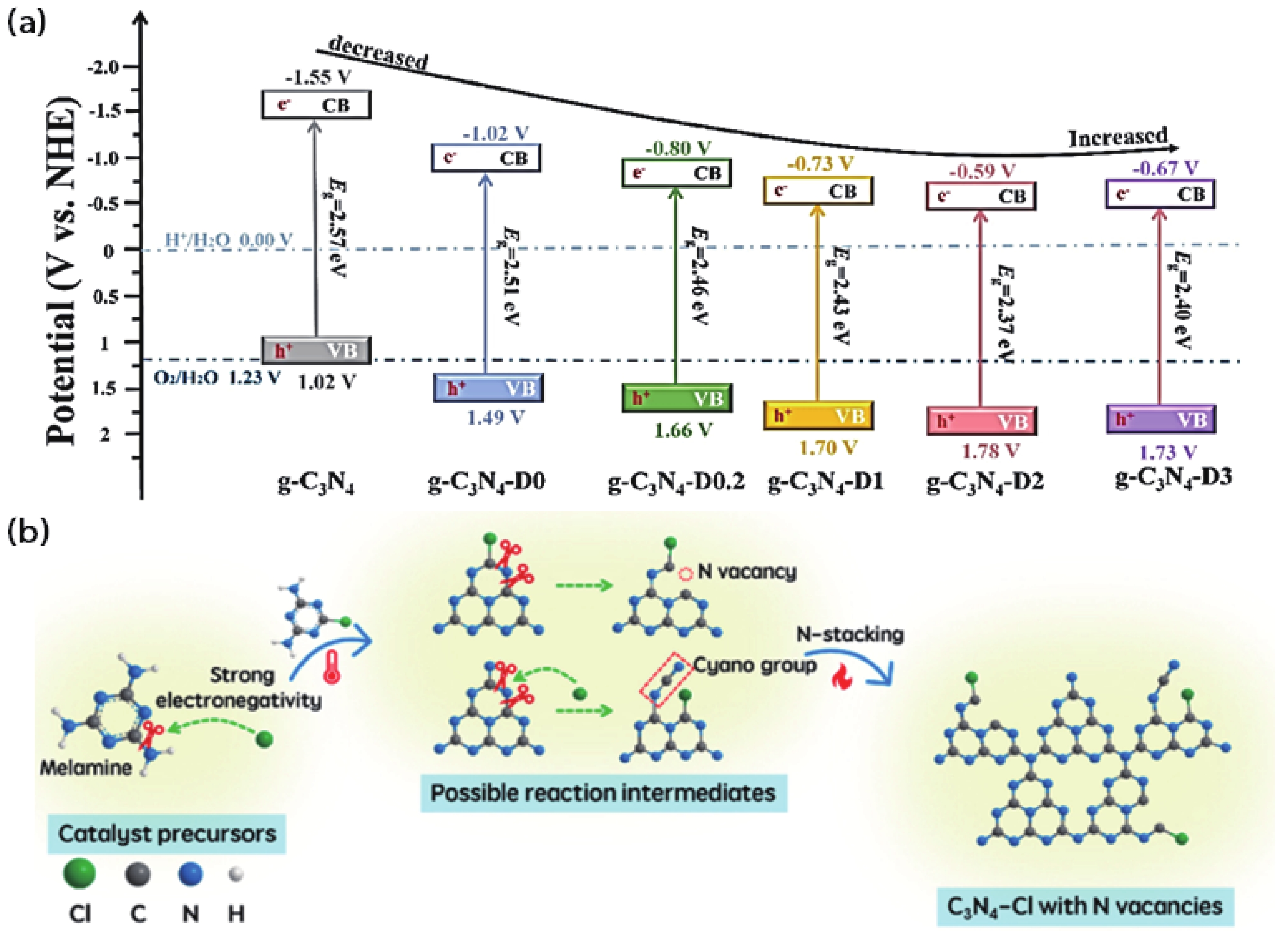
Developing low-cost, efficient, and stable photocatalysts is one of the most promising methods for large-scale solar water splitting. As a metal-free semiconductor material with suitable band gap, graphitic carbon nitride (g-C3N4) has attracted attention in the field of photocatalysis, which is mainly attributed to its fascinating physicochemical and photoelectronic properties. However, several inherent limitations and shortcomings—involving high recombination rate of photocarriers, insufficient reaction kinetics, and optical absorption—impede the practical applicability of g-C3N4. As an effective strategy, vacancy defect engineering has been widely used for breaking through the current limitations, considering its ability to optimize the electronic structure and surface morphology of g-C3N4 to obtain the desired photocatalytic activity. This review summarizes the recent progress of vacancy defect engineered g-C3N4 for solar water splitting. The fundamentals of solar water splitting with g-C3N4 are discussed first. We then focus on the fabrication strategies and effect of vacancy generated in g-C3N4. The advances of vacancy-modified g-C3N4 photocatalysts toward solar water splitting are discussed next. Finally, the current challenges and future opportunities of vacancy-modified g-C3N4 are summarized. This review aims to provide a theoretical basis and guidance for future research on the design and development of highly efficient defective g-C3N4.


J. Semicond.
2023, 44(8): 082001 doi: 10.1088/1674-4926/44/8/082001
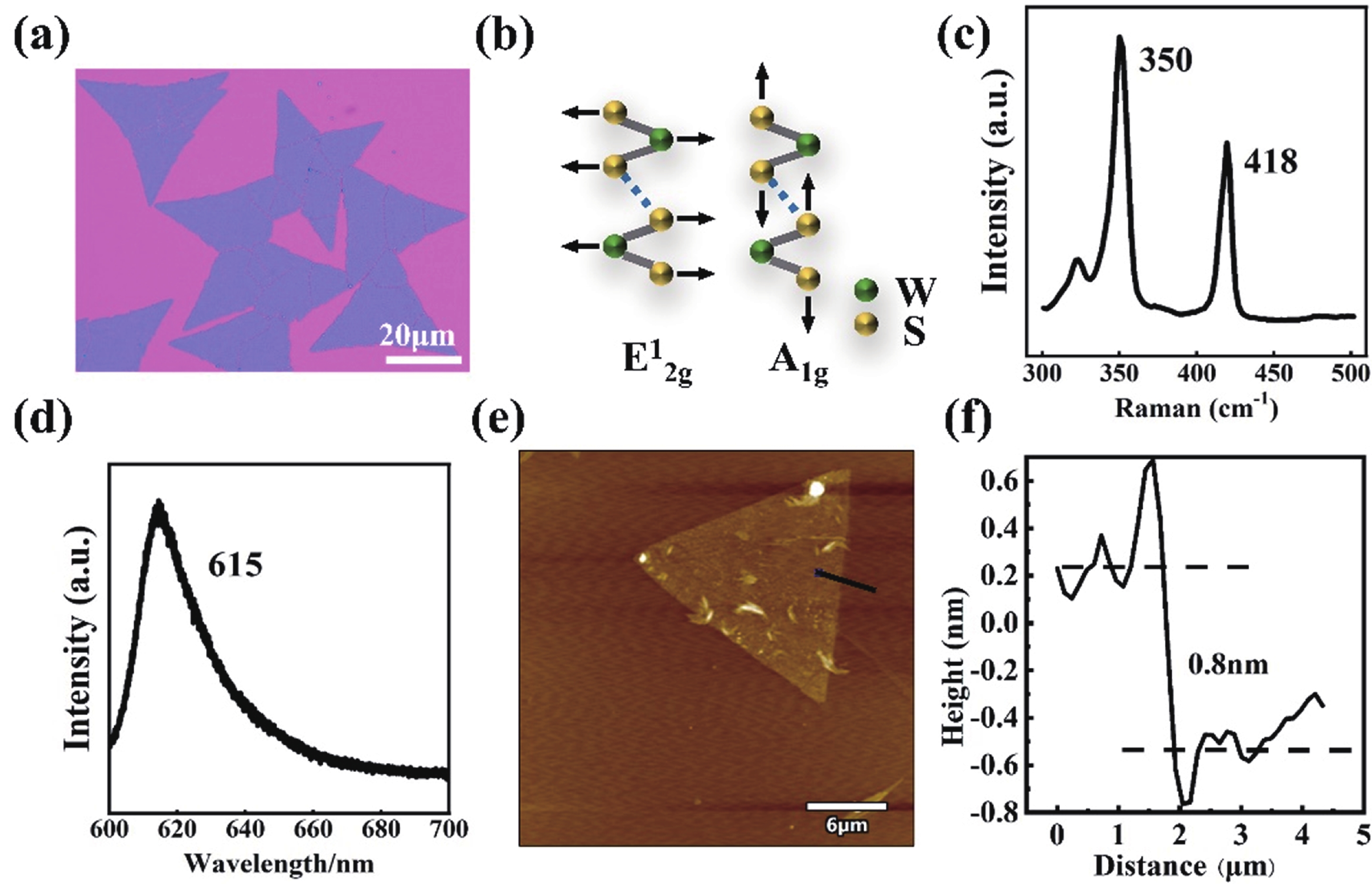
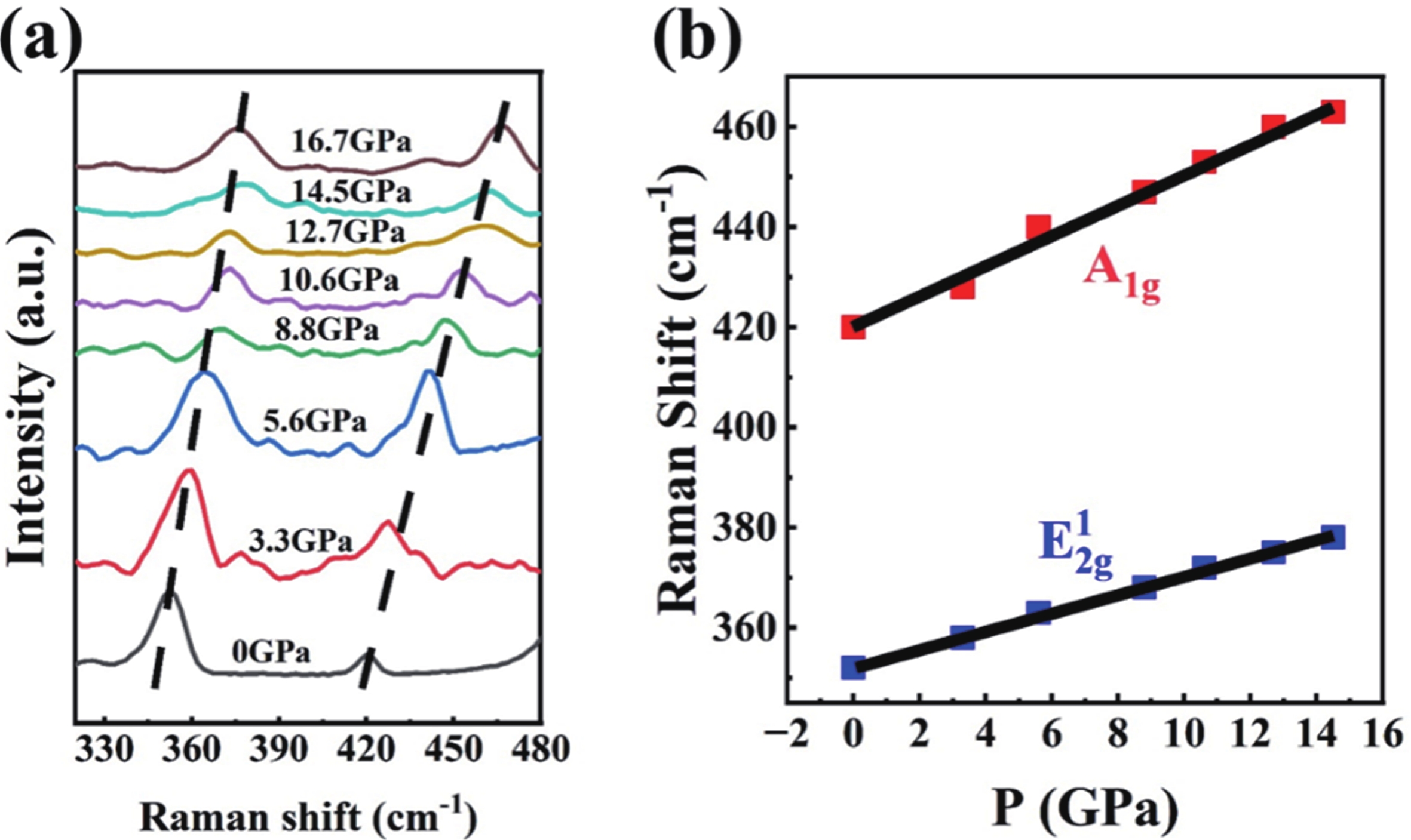
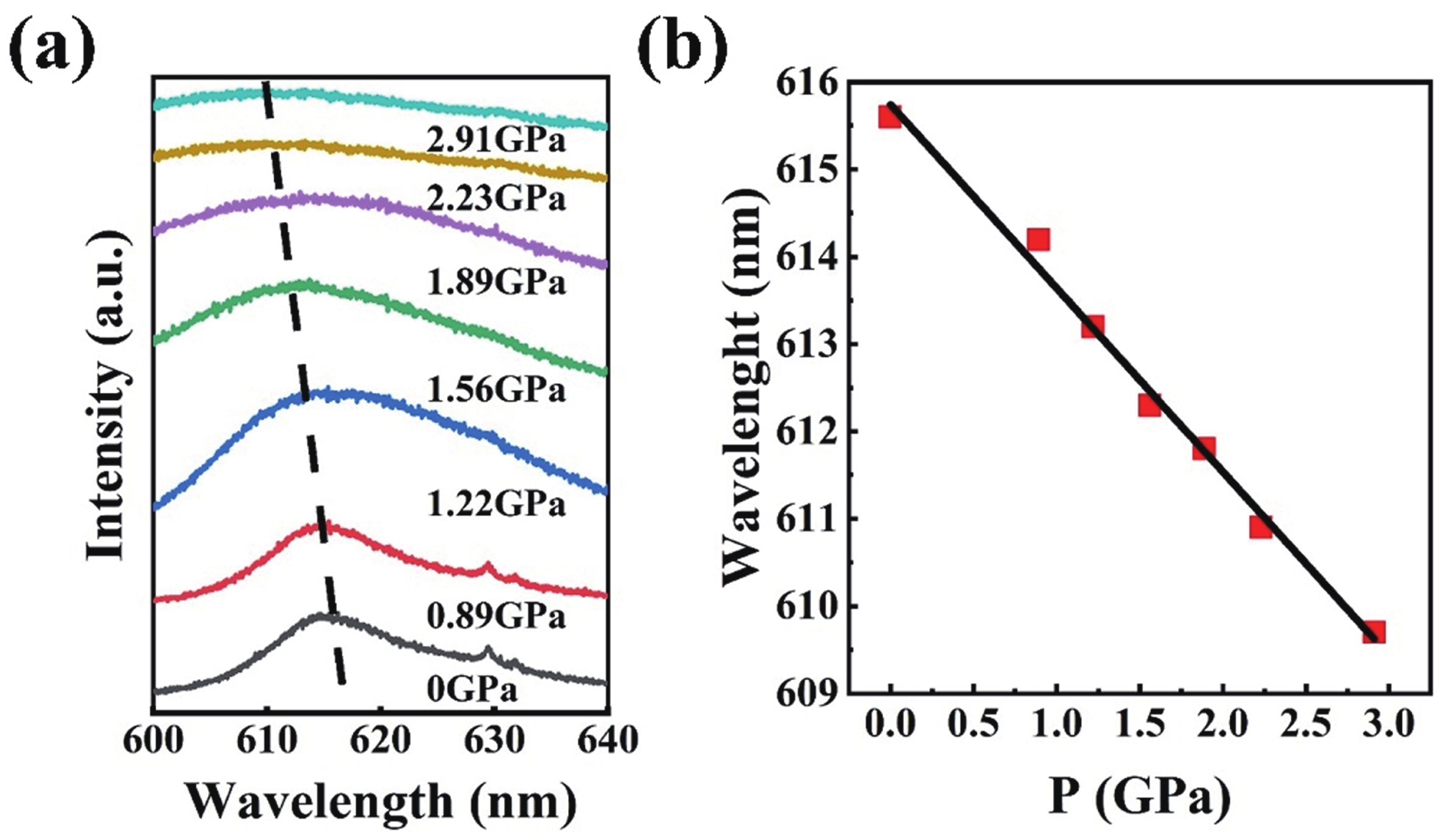
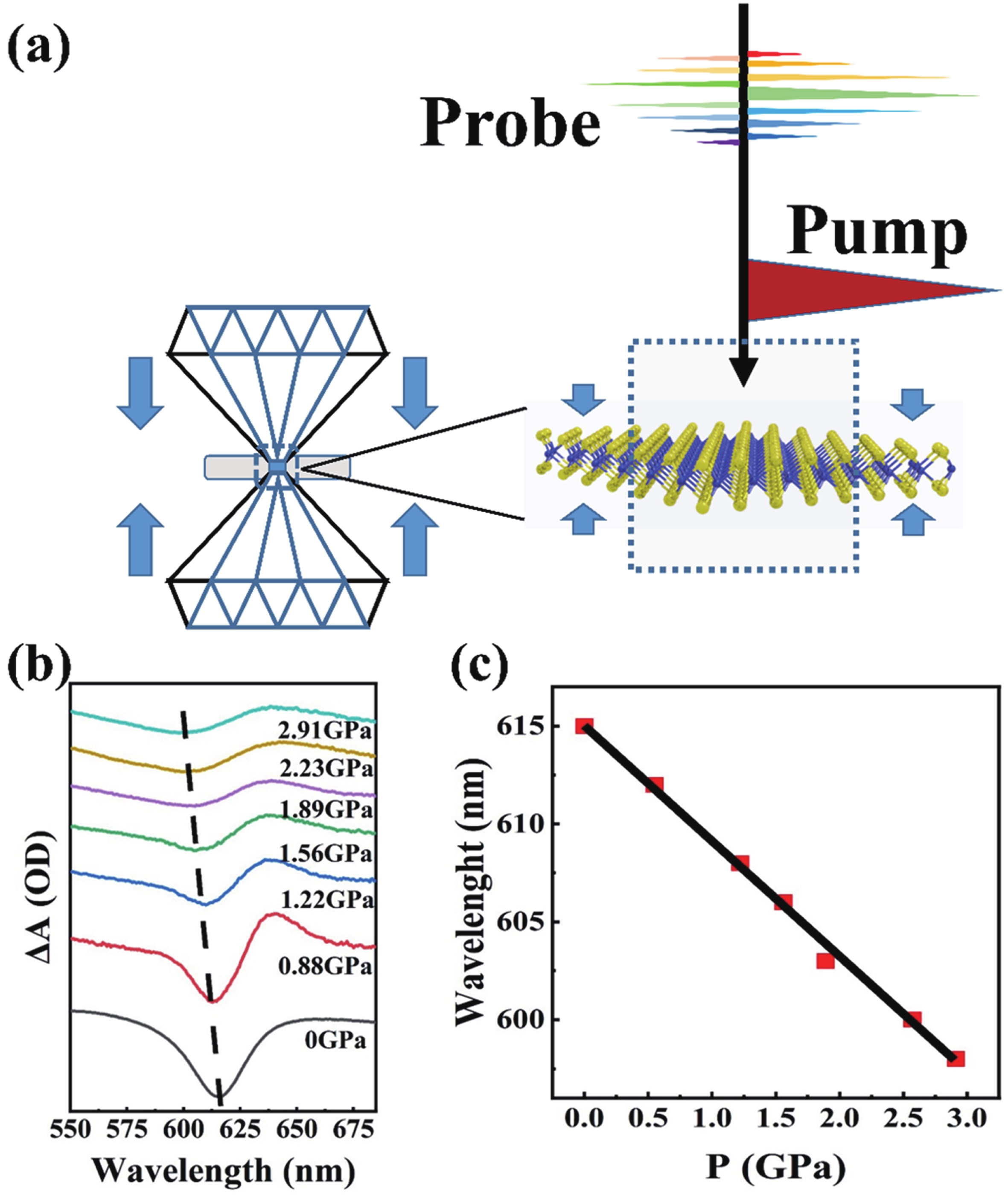
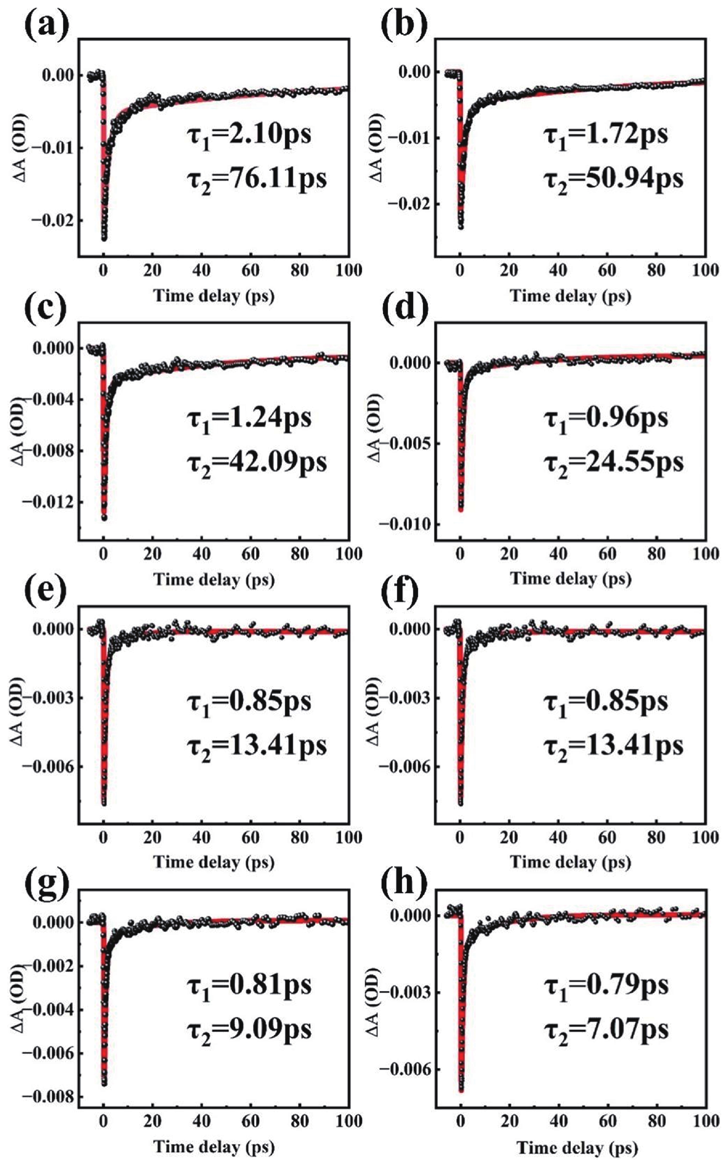
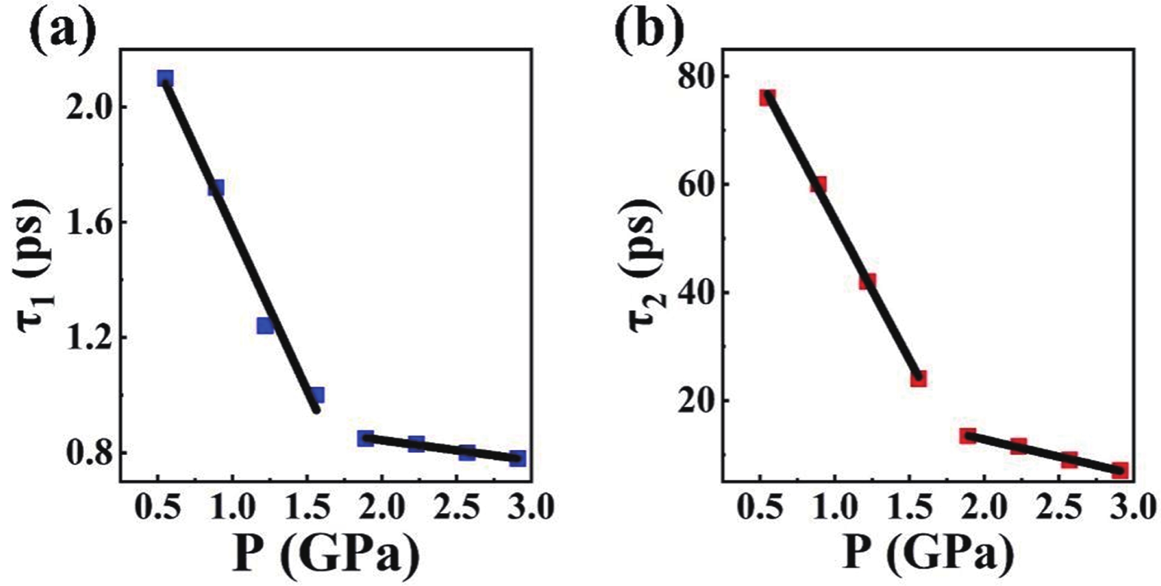
Two-dimensional transition metal dichalcogenides (TMDs) have intriguing physic properties and offer an exciting platform to explore many features that are important for future devices. In this work, we synthesized monolayer WS2 as an example to study the optical response with hydrostatic pressure. The Raman results show a continuous tuning of the lattice vibrations that is induced by hydrostatic pressure. We further demonstrate an efficient pressure-induced change of the band structure and carrier dynamics via transient absorption measurements. We found that two time constants can be attributed to the capture process of two kinds of defect states, with the pressure increasing from 0.55 GPa to 2.91 GPa, both of capture processes were accelerated, and there is an inflection point within the pressure range of 1.56 GPa to 1.89 GPa. Our findings provide valuable information for the design of future optoelectronic devices.

J. Semicond.
2023, 44(8): 082201 doi: 10.1088/1674-4926/44/8/082201
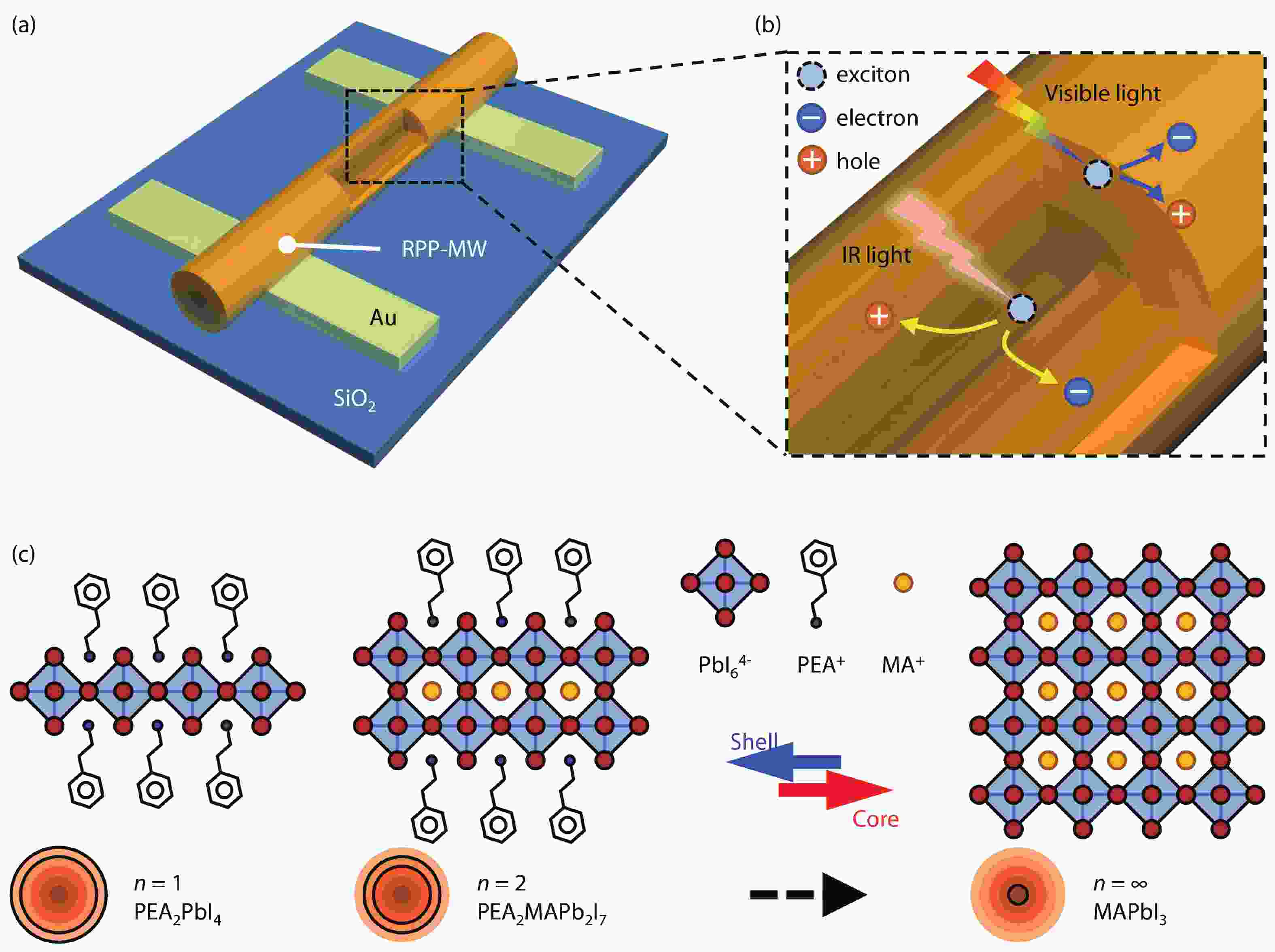
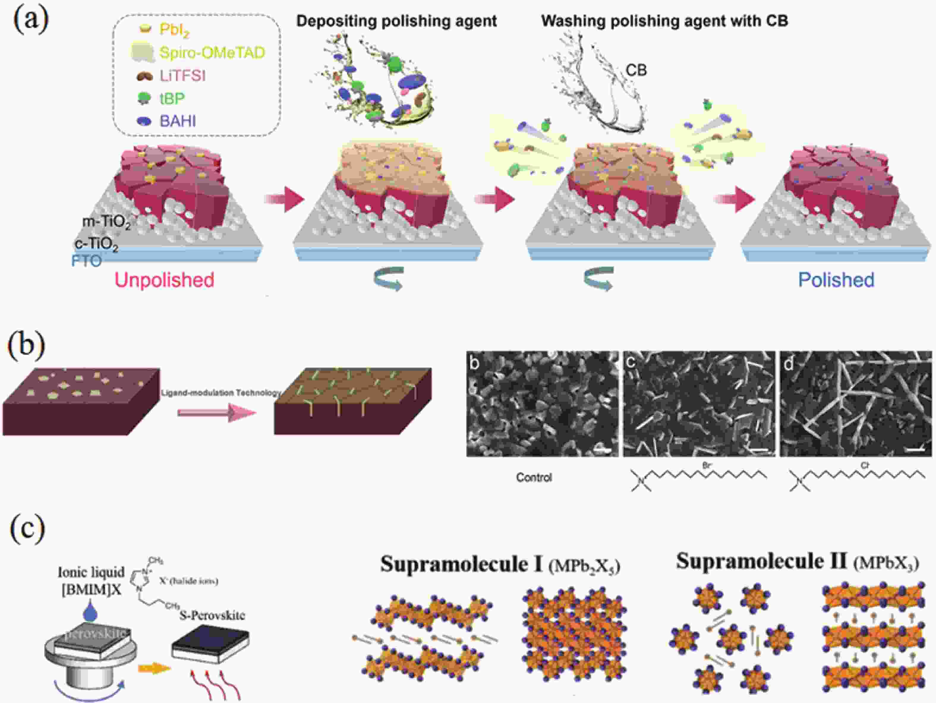
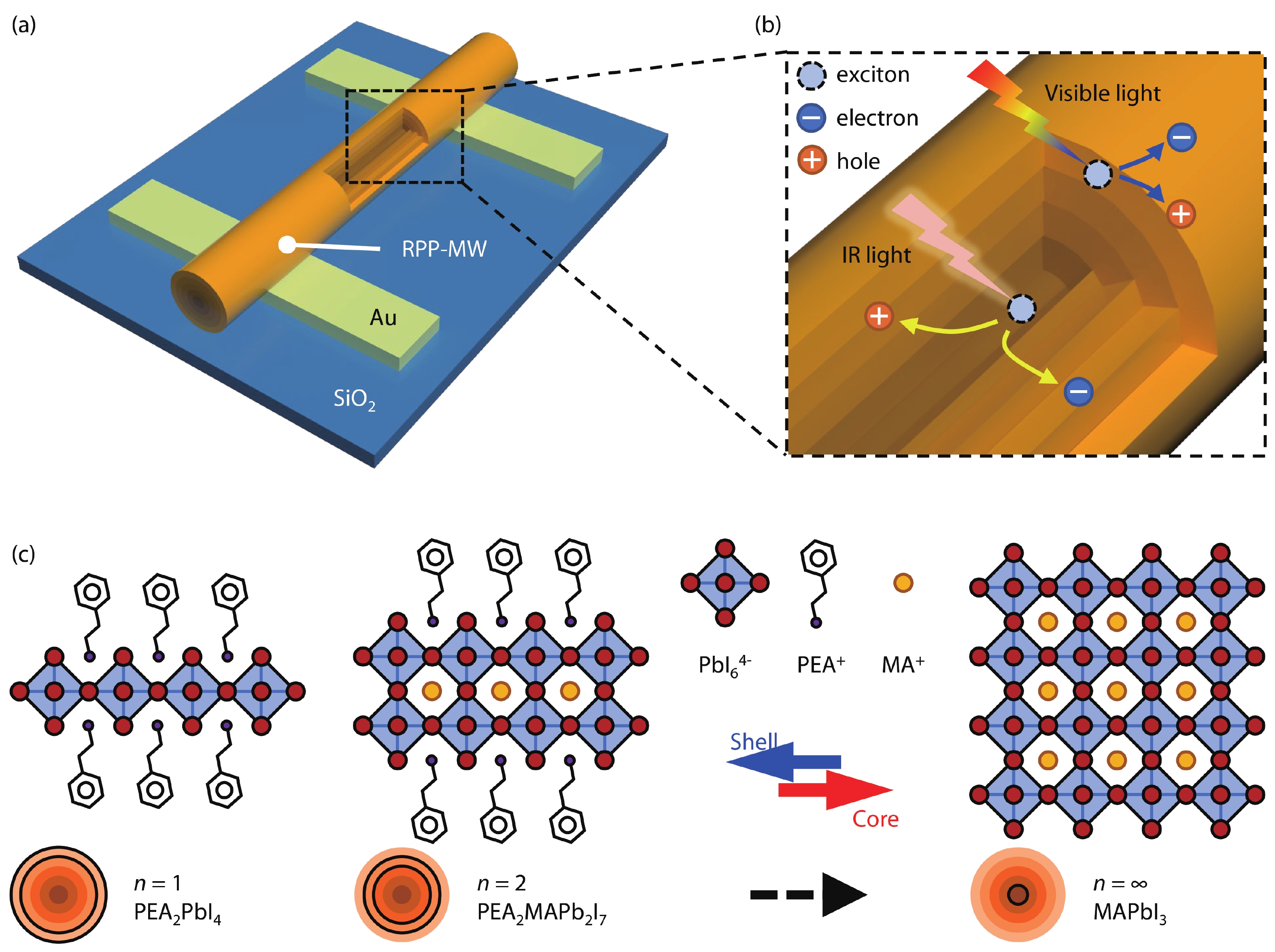
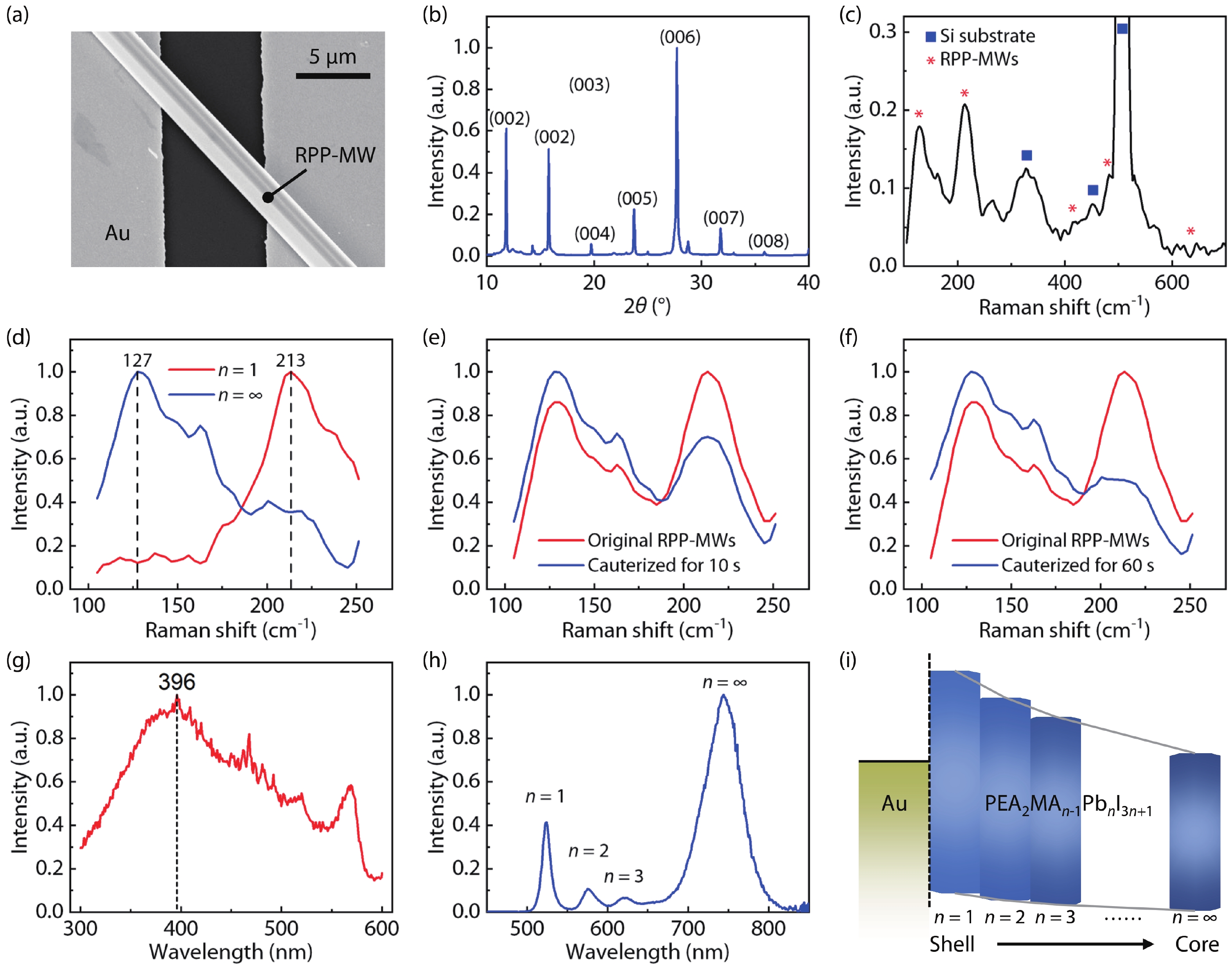
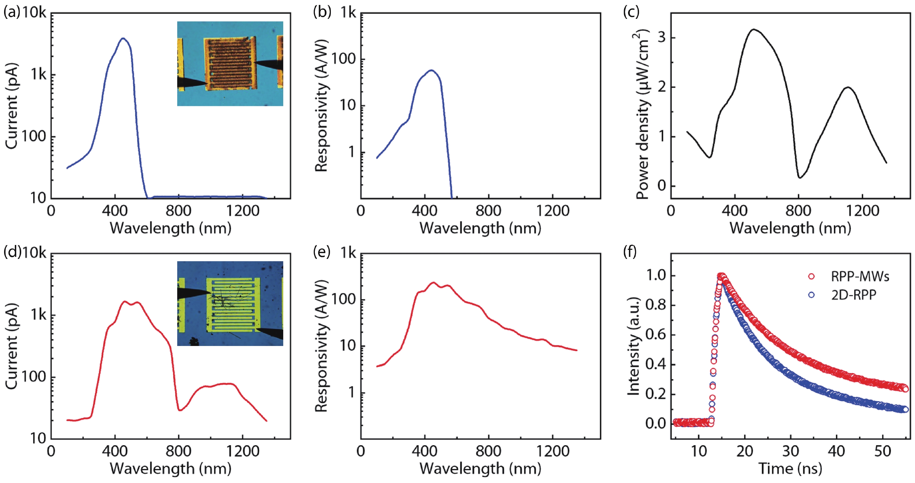
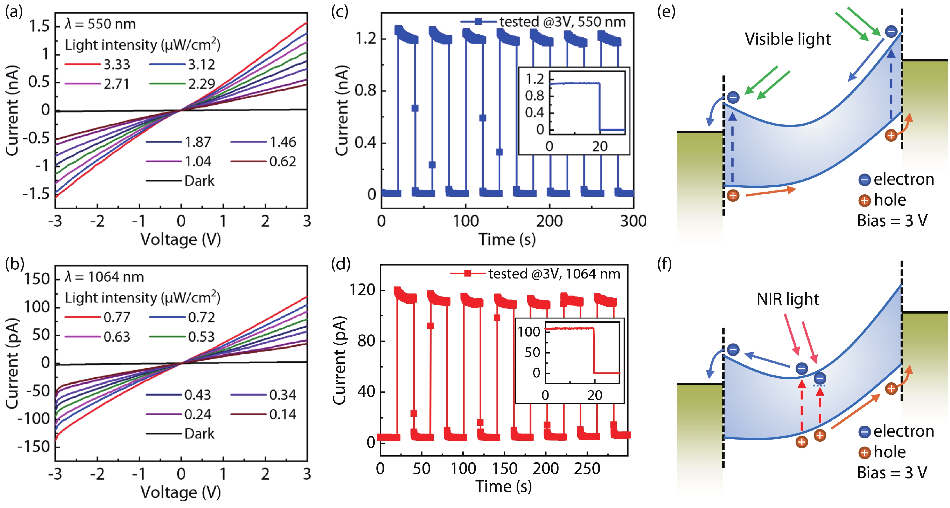
Recently, the two-dimensional (2D) form of Ruddlesden-Popper perovskite (RPP) has been widely studied. However, the synthesis of one-dimensional (1D) RPP is rarely reported. Here, we fabricated a photodetector based on RPP microwires (RPP-MWs) and compared it with a 2D-RPP photodetector. The results show that the RPP-MWs photodetector possesses a wider photoresponse range and higher responsivities of 233 A/W in the visible band and 30 A/W in the near-infrared (NIR) band. The analyses show that the synthesized RPP-MWs have a multi-layer, heterogeneous core-shell structure. This structure gives RPP-MWs a unique band structure, as well as abundant trap states and defect levels, which enable them to acquire better photoresponse performance. This configuration of RPP-MWs provides a new idea for the design and application of novel heterostructures.
J. Semicond.
2023, 44(8): 082202 doi: 10.1088/1674-4926/44/8/082202
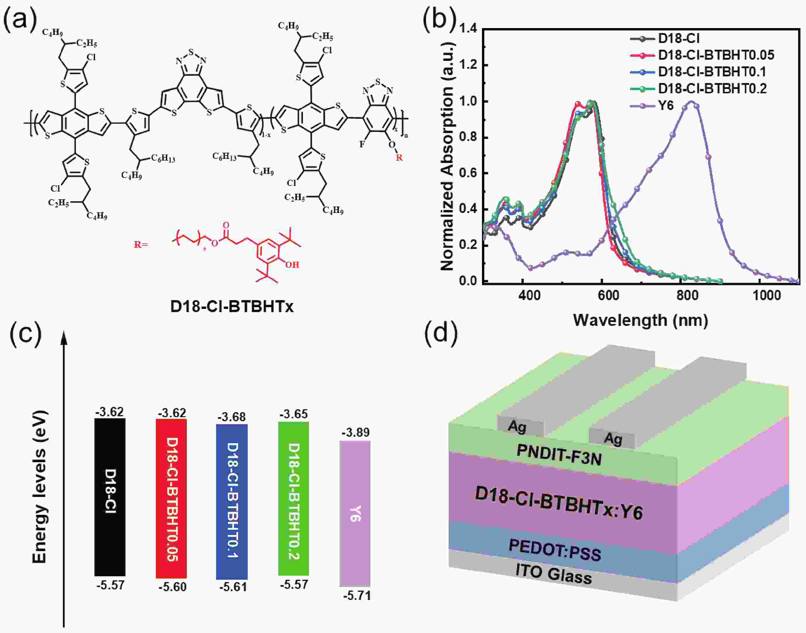
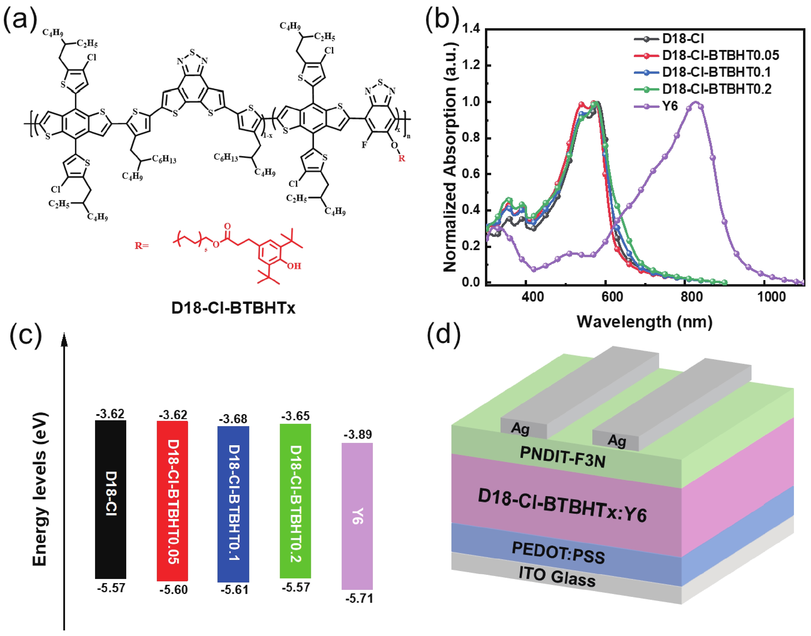
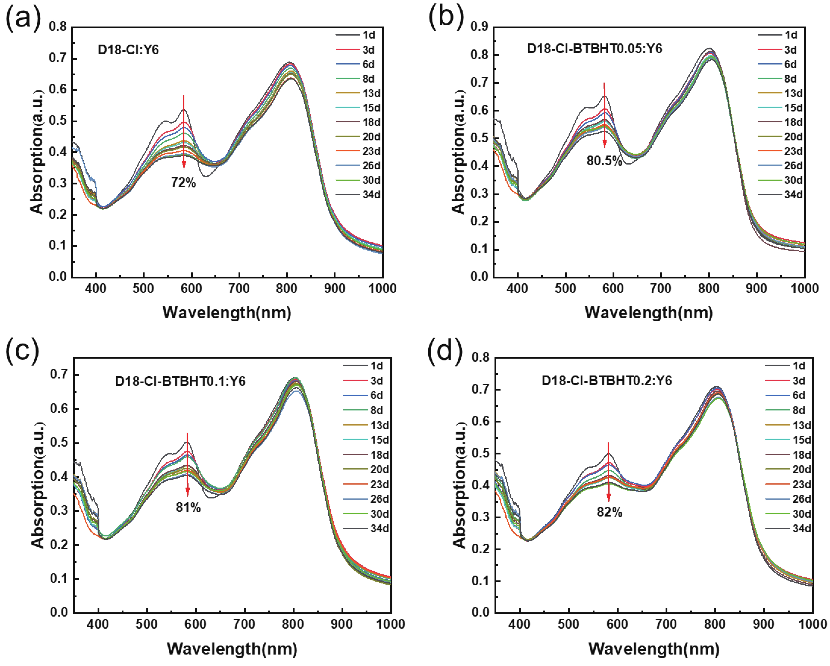
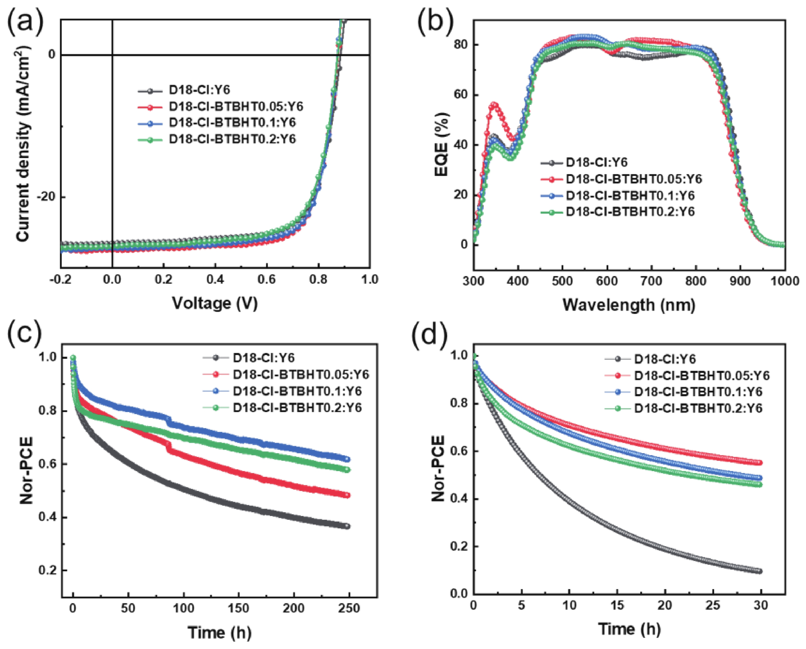
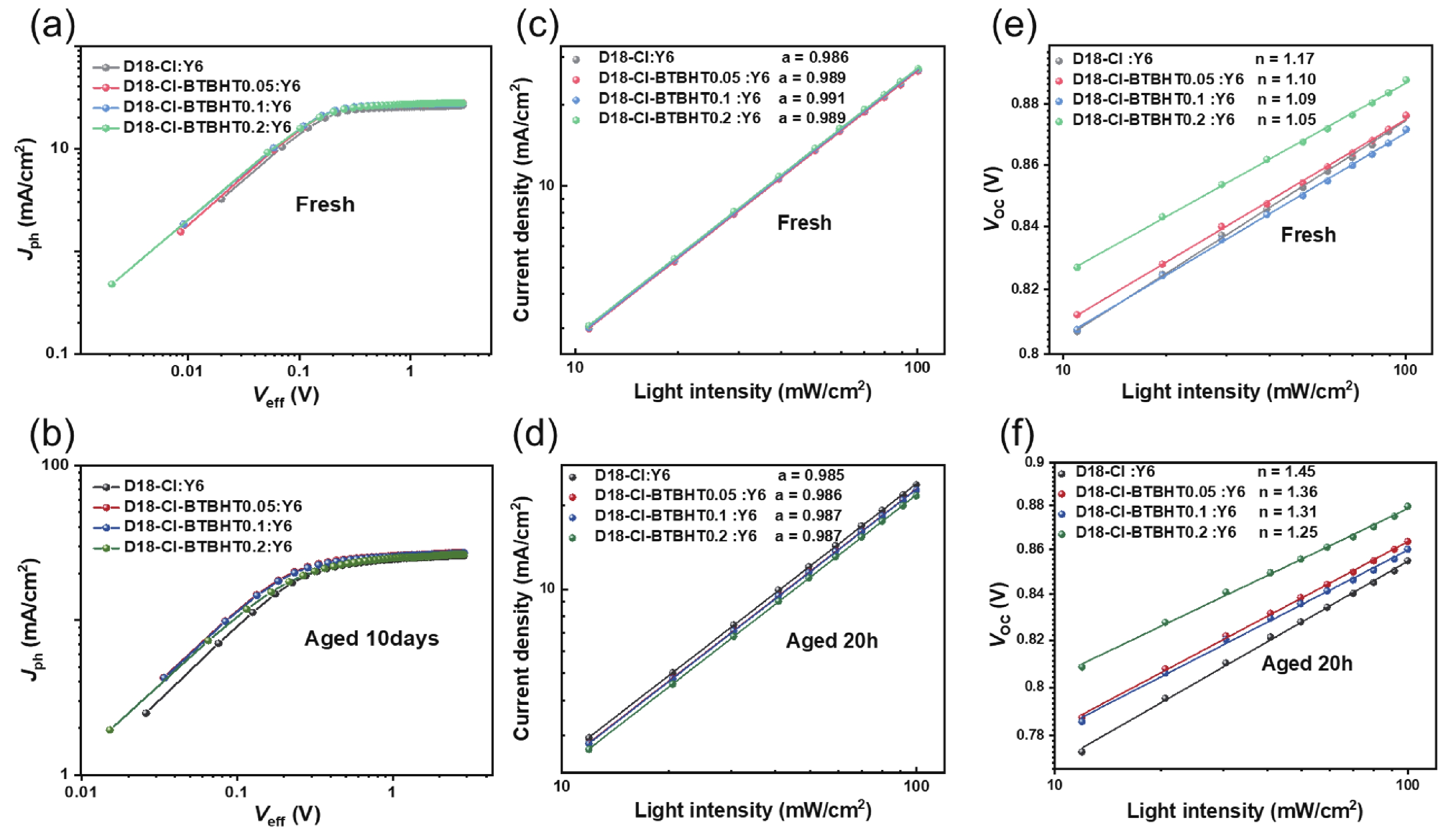
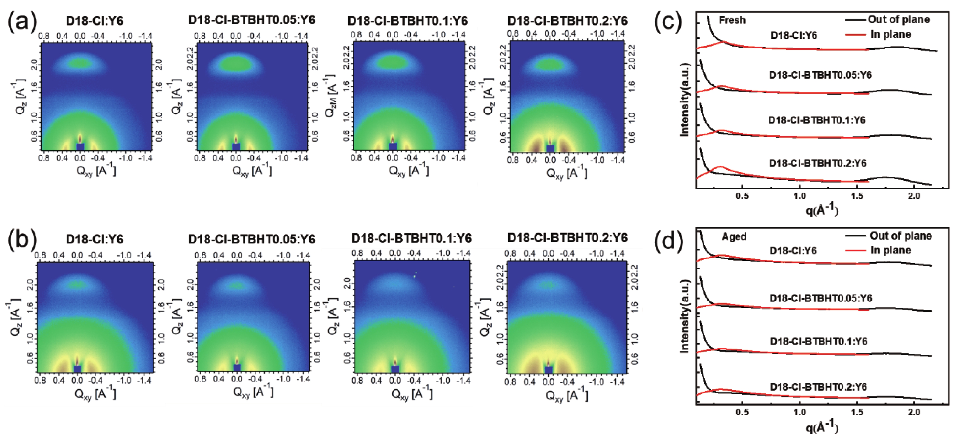
The stability of organic solar cells (OSCs) remains a major concern for their ultimate industrialization due to the photo, oxygen, and water susceptibility of organic photoactive materials. Usually, antioxidant additives are blended as radical scavengers into the active layer. However, it will induce the intrinsic morphology instability and adversely affect the efficiency and long-term stability. Herein, the antioxidant dibutylhydroxytoluene (BHT) group has been covalently linked onto the side chain of benzothiadiazole (BT) unit, and a series of ternary copolymers D18-Cl-BTBHTx (x = 0, 0.05, 0.1, 0.2) with varied ratio of BHT-containing side chains have been synthesized. It was found that the introduction of BHT side chains would have a negligible effect on the photophysical properties and electronic levels, and the D18-Cl-BTBHT0.05: Y6-based OSC achieved the highest power conversion efficiency (PCE) of 17.6%, which is higher than those based active layer blended with BHT additives. More importantly, the unencapsulated device based on D18-Cl-BTBHTx (x = 0.05, 0.1, 0.2) retained approximately 50% of the initial PCE over 30 hours operation under ambient conditions, significantly outperforming the control device based on D18-Cl (90% degradation in PCE after 30 h). This work provides a new structural design strategy of copolymers for OSCs with simultaneously improved efficiency and stability.

J. Semicond.
2023, 44(8): 082501 doi: 10.1088/1674-4926/44/8/082501
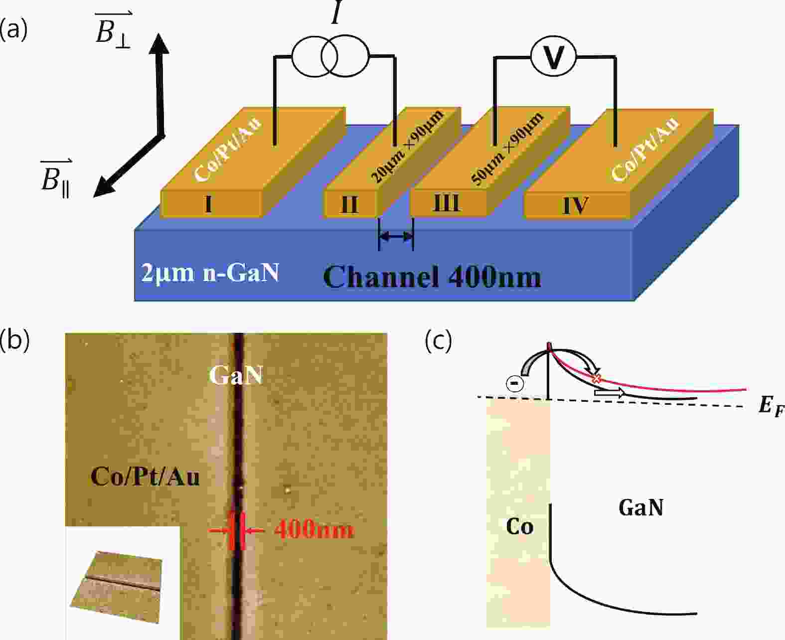
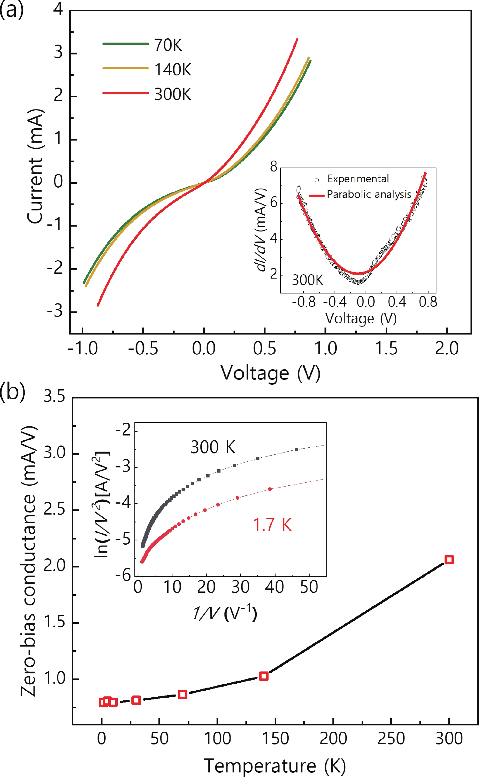
Spin injection and detection in bulk GaN were investigated by performing magnetotransport measurements at low temperatures. A non-local four-terminal lateral spin valve device was fabricated with Co/GaN Schottky contacts. The spin injection efficiency of 21% was achieved at 1.7 K. It was confirmed that the thin Schottky barrier formed between the heavily n-doped GaN and Co was conducive to the direct spin tunneling, by reducing the spin scattering relaxation through the interface states.


J. Semicond.
2023, 44(8): 082701 doi: 10.1088/1674-4926/44/8/082701
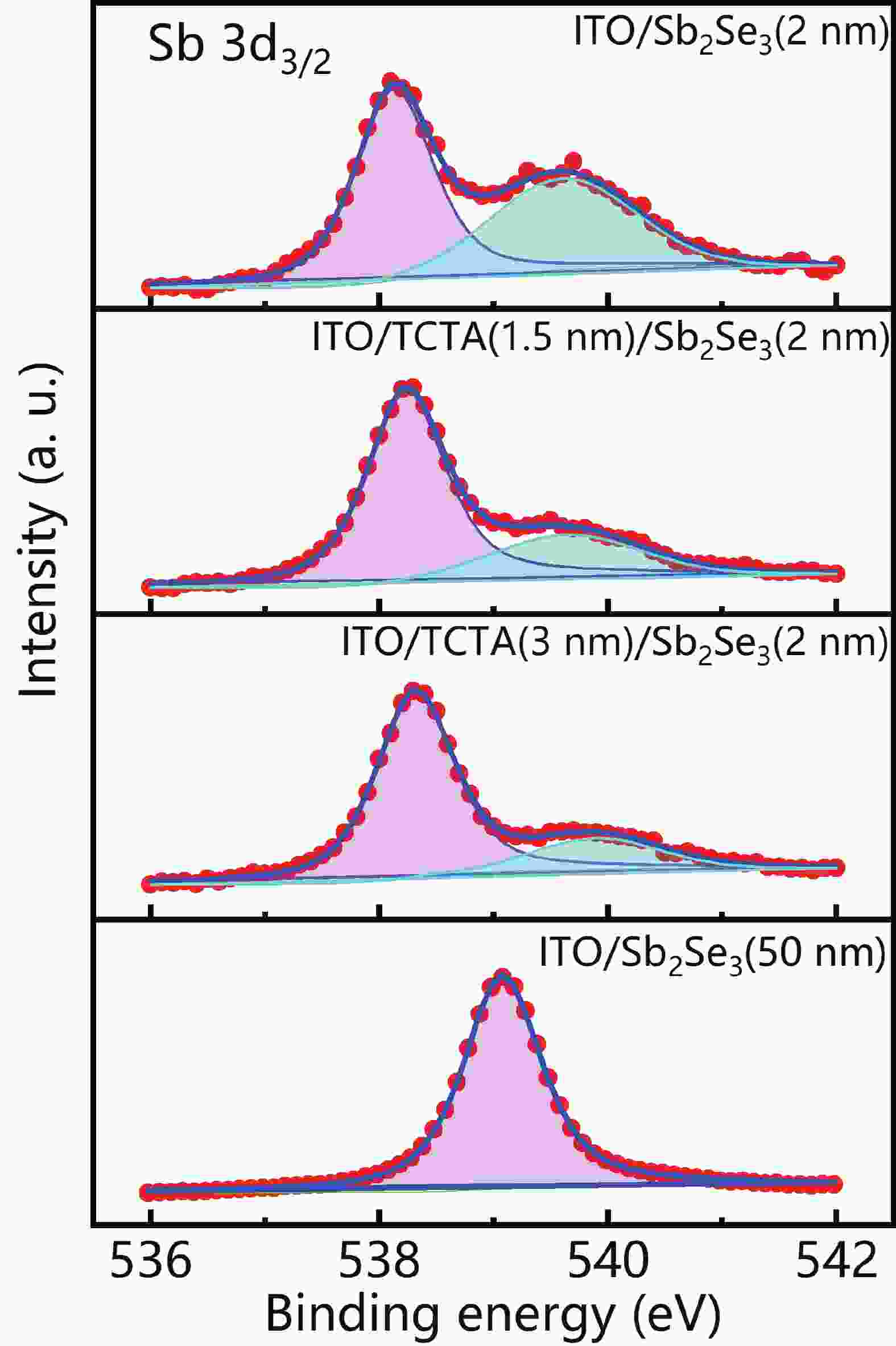
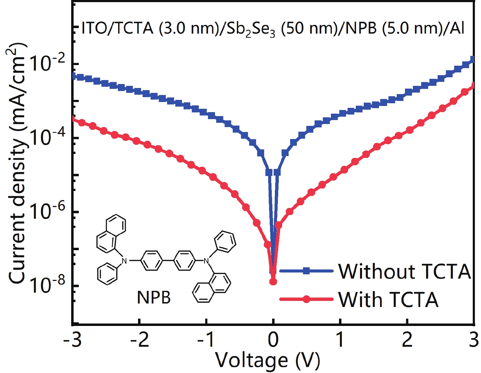
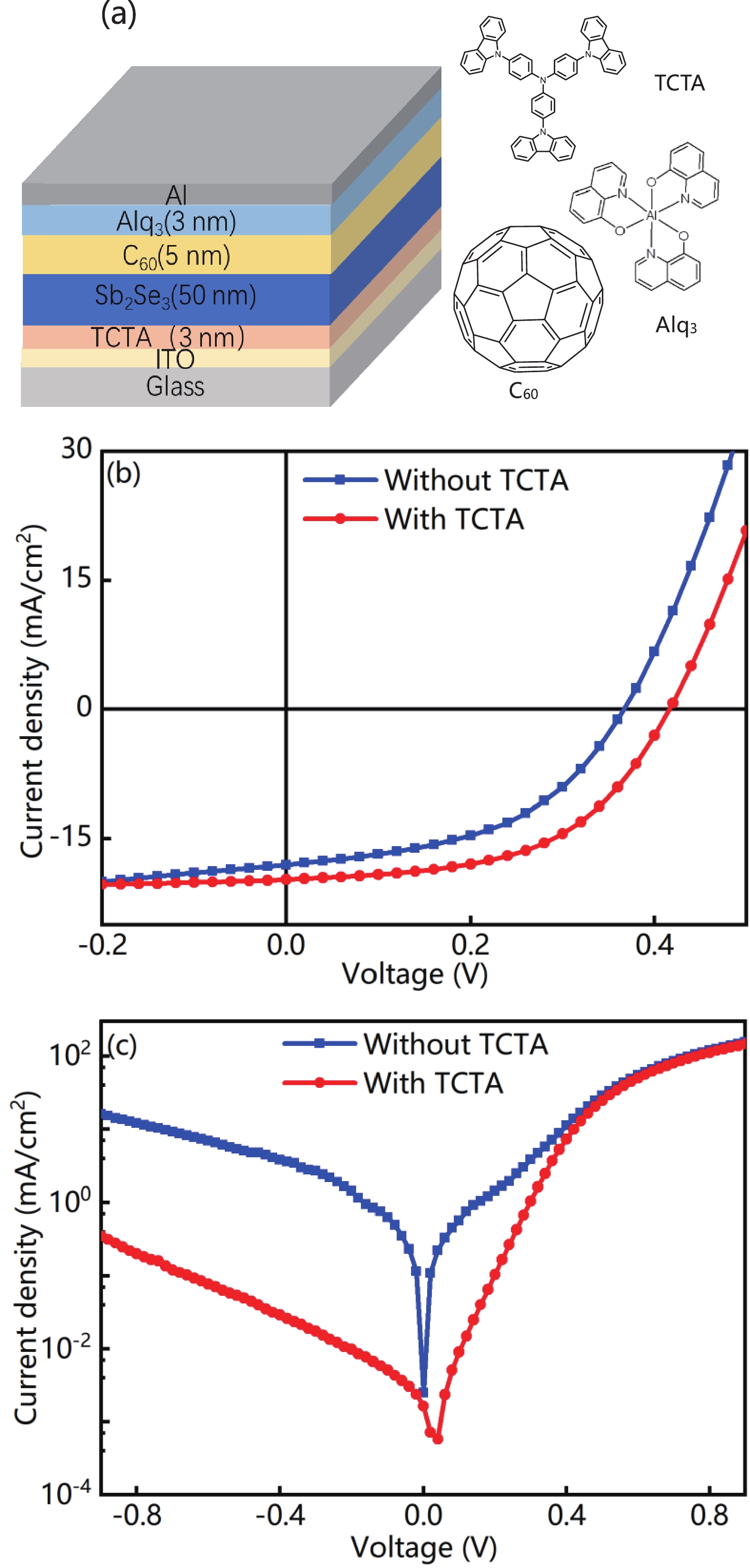
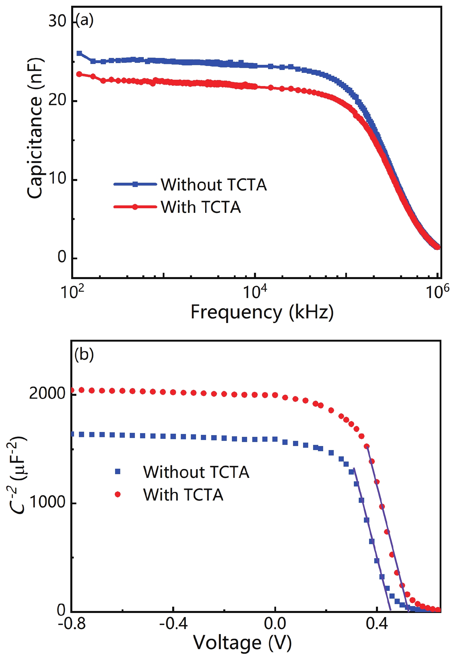
Antimony selenide (Sb2Se3) is an emerging solar cell material. Here, we demonstrate that an organic small molecule of 4, 4', 4''-tris(carbazol-9-yl)-triphenylamine (TCTA) can efficiently passivate the anode interface of the Sb2Se3 solar cell. We fabricated the device by the vacuum thermal evaporation, and took ITO/TCTA (3.0 nm)/Sb2Se3 (50 nm)/C60 (5.0 nm)/Alq3 (3.0 nm)/Al as the device architecture, where Alq3 is the tris(8-hydroxyquinolinato) aluminum. By introducing a TCTA layer, the open-circuit voltage is raised from 0.36 to 0.42 V, and the power conversion efficiency is significantly improved from 3.2% to 4.3%. The TCTA layer not only inhibits the chemical reaction between the ITO and Sb2Se3 during the annealing process but it also blocks the electron diffusion from Sb2Se3 to ITO anode. The enhanced performance is mainly attributed to the suppression of the charge recombination at the anode interface.


J. Semicond.
2023, 44(8): 082702 doi: 10.1088/1674-4926/44/8/082702
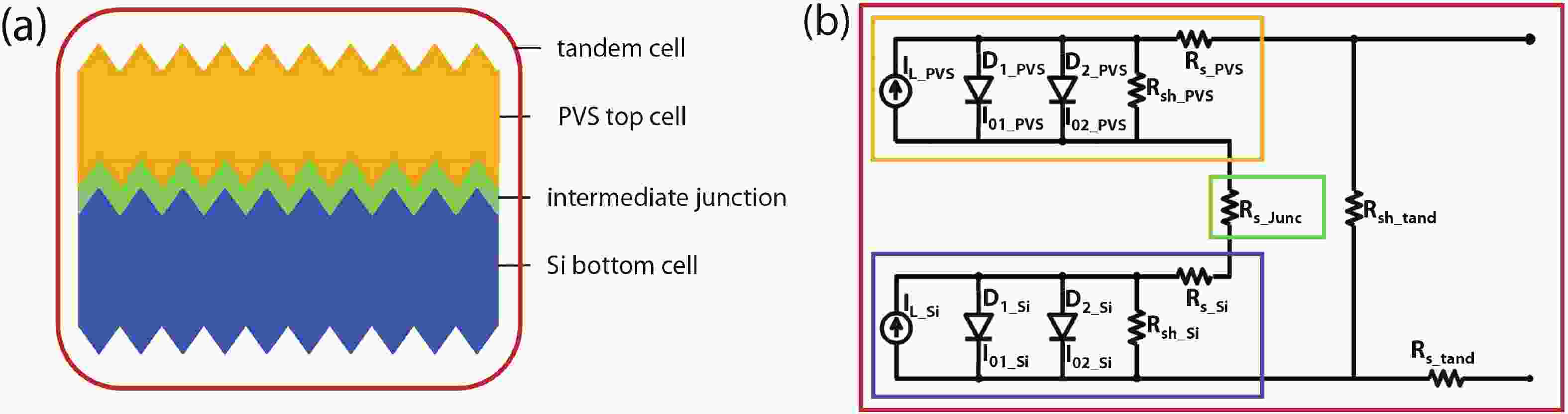
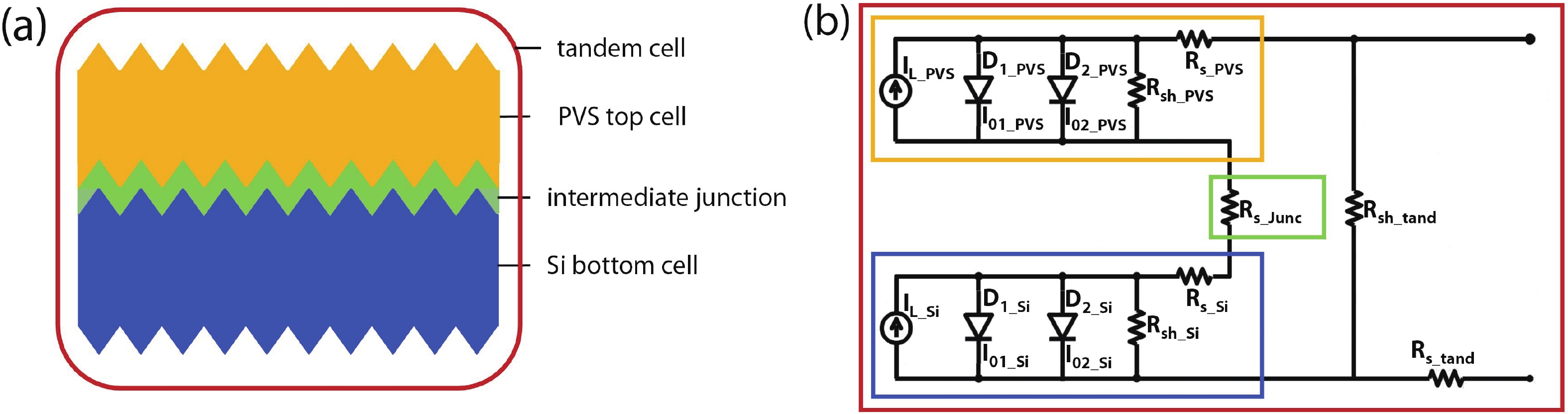
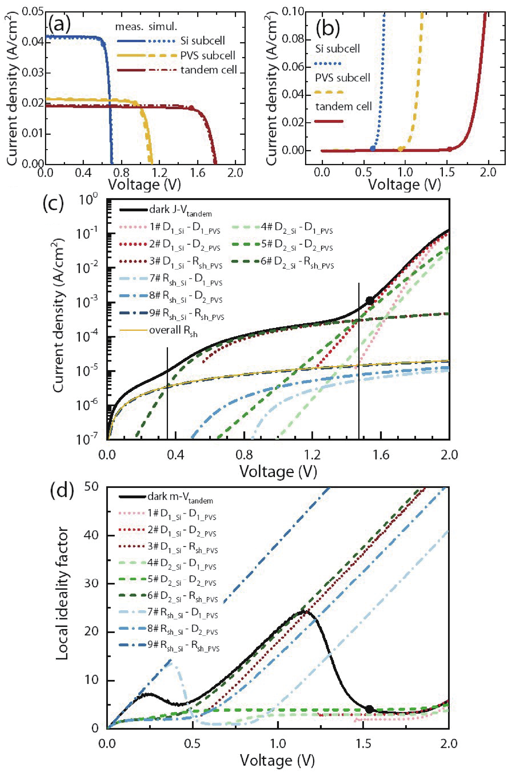
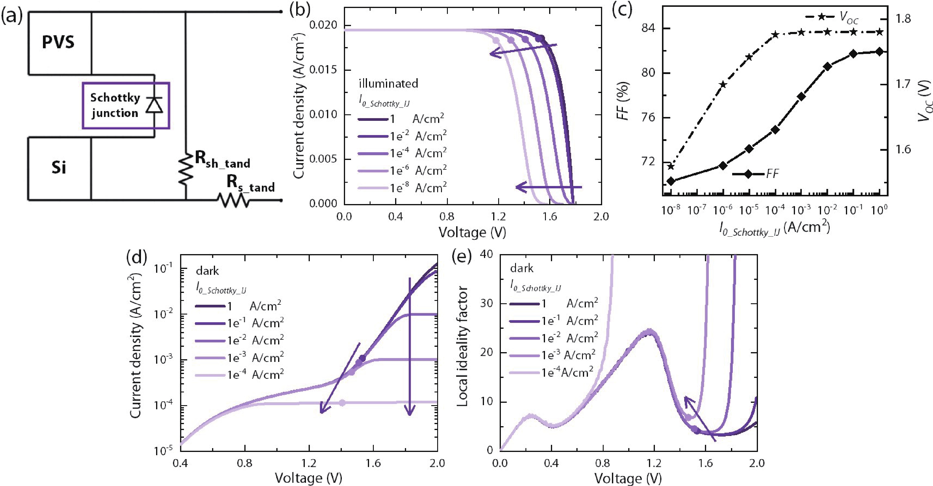
In this work, we developed a simple and direct circuit model with a dual two-diode model that can be solved by a SPICE numerical simulation to comprehensively describe the monolithic perovskite/crystalline silicon (PVS/c-Si) tandem solar cells. We are able to reveal the effects of different efficiency-loss mechanisms based on the illuminated current density-voltage (J-V), semi-log dark J-V, and local ideality factor (m-V) curves. The effects of the individual efficiency-loss mechanism on the tandem cell’s efficiency are discussed, including the exp(V/VT) and exp(V/2VT) recombination, the whole cell’s and subcell’s shunts, and the Ohmic-contact or Schottky-contact of the intermediate junction. We can also fit a practical J-V curve and find a specific group of parameters by the trial-and-error method. Although the fitted parameters are not a unique solution, they are valuable clues for identifying the efficiency loss with the aid of the cell’s structure and experimental processes. This method can also serve as an open platform for analyzing other tandem solar cells by substituting the corresponding circuit models. In summary, we developed a simple and effective methodology to diagnose the efficiency-loss source of a monolithic PVS/c-Si tandem cell, which is helpful to researchers who wish to adopt the proper approaches to improve their solar cells.


J. Semicond.
2023, 44(8): 082801 doi: 10.1088/1674-4926/44/8/082801
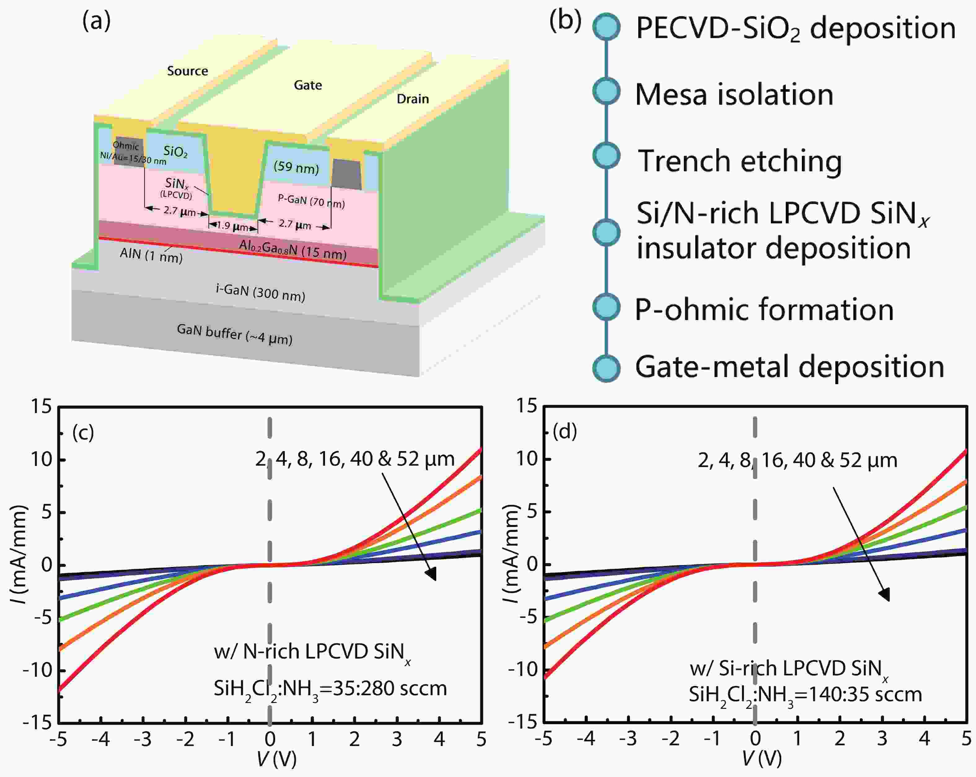
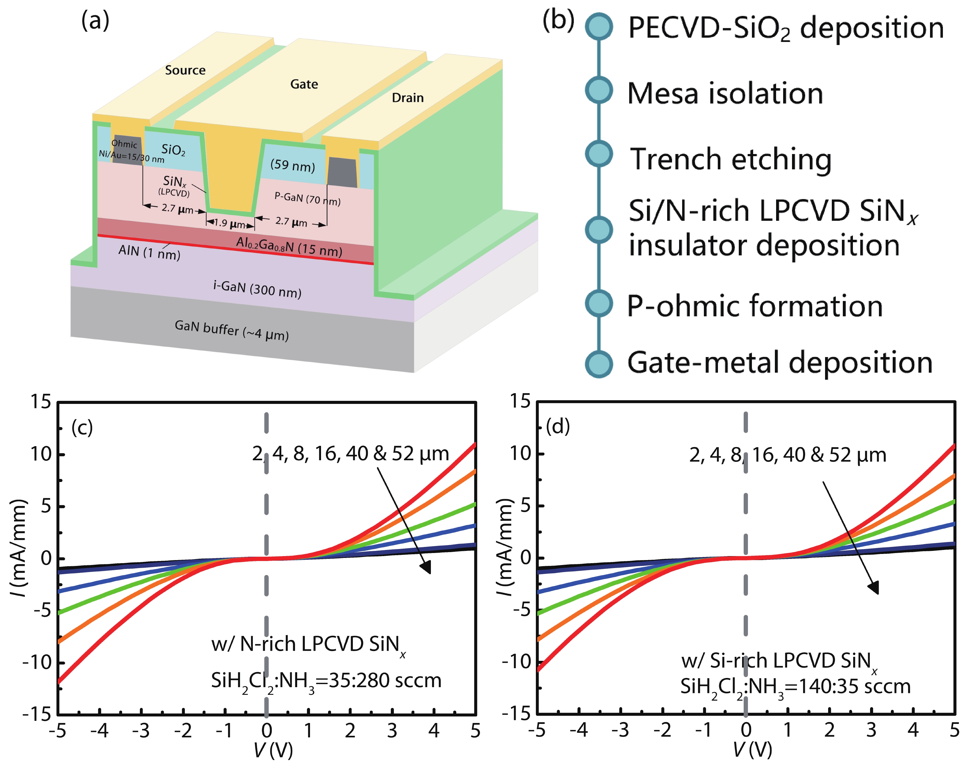
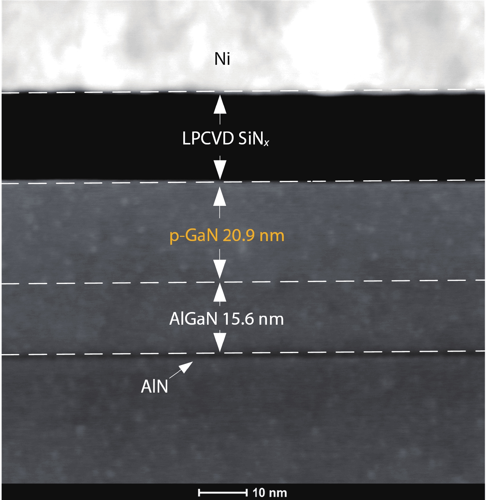
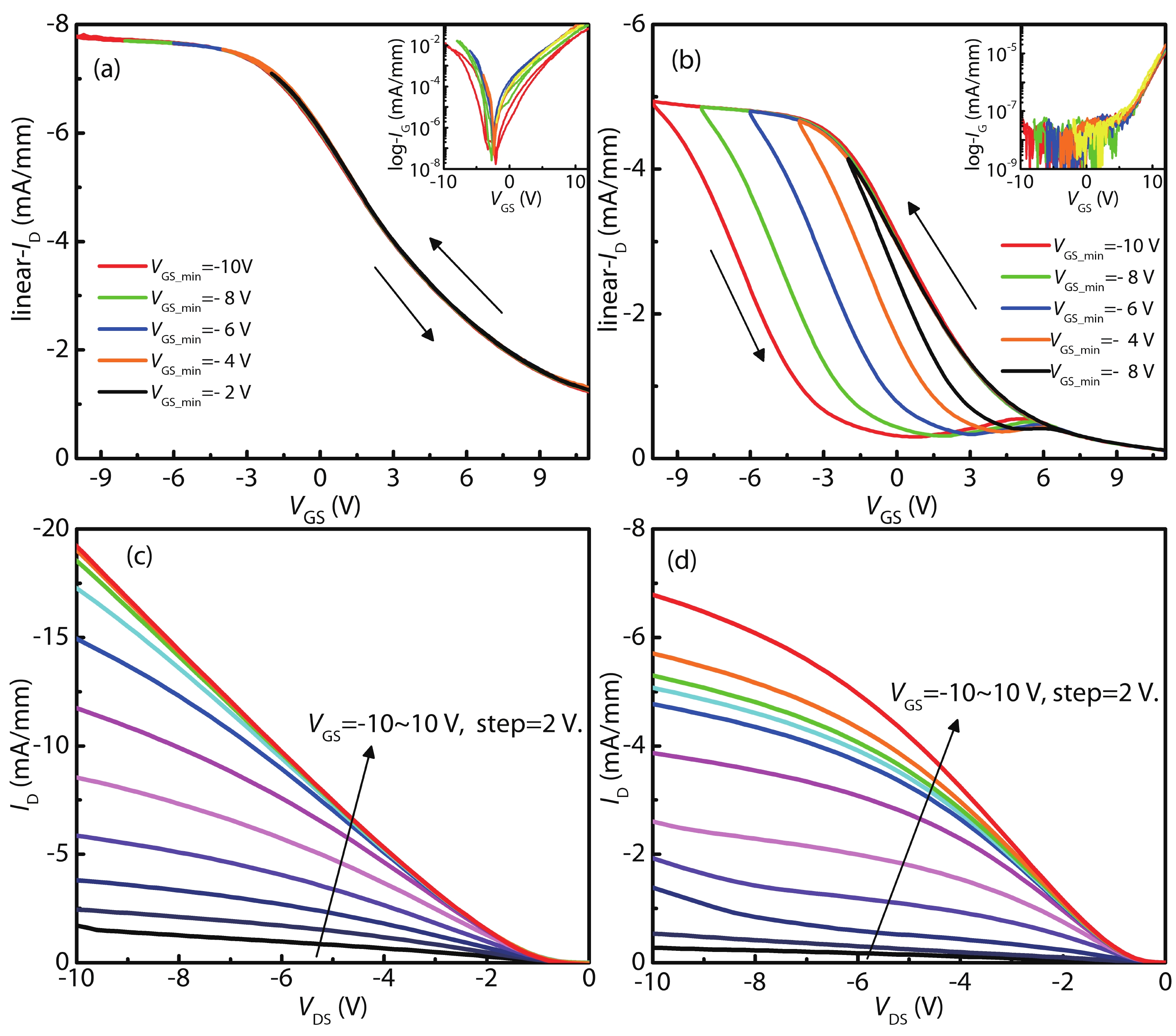
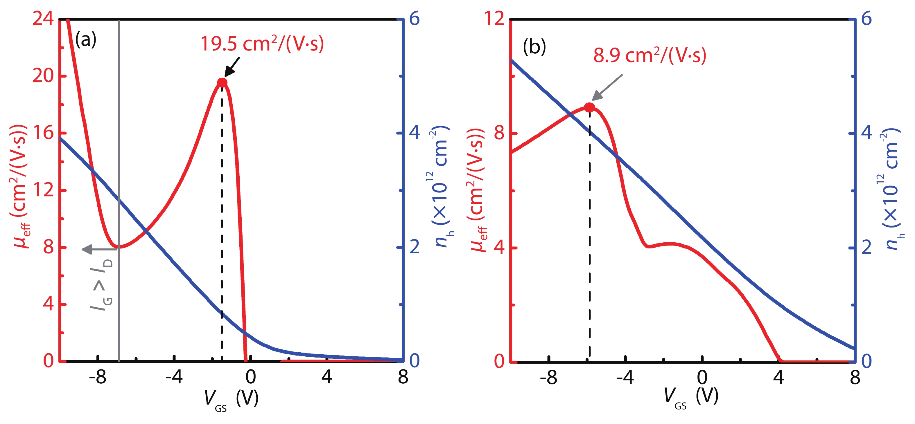
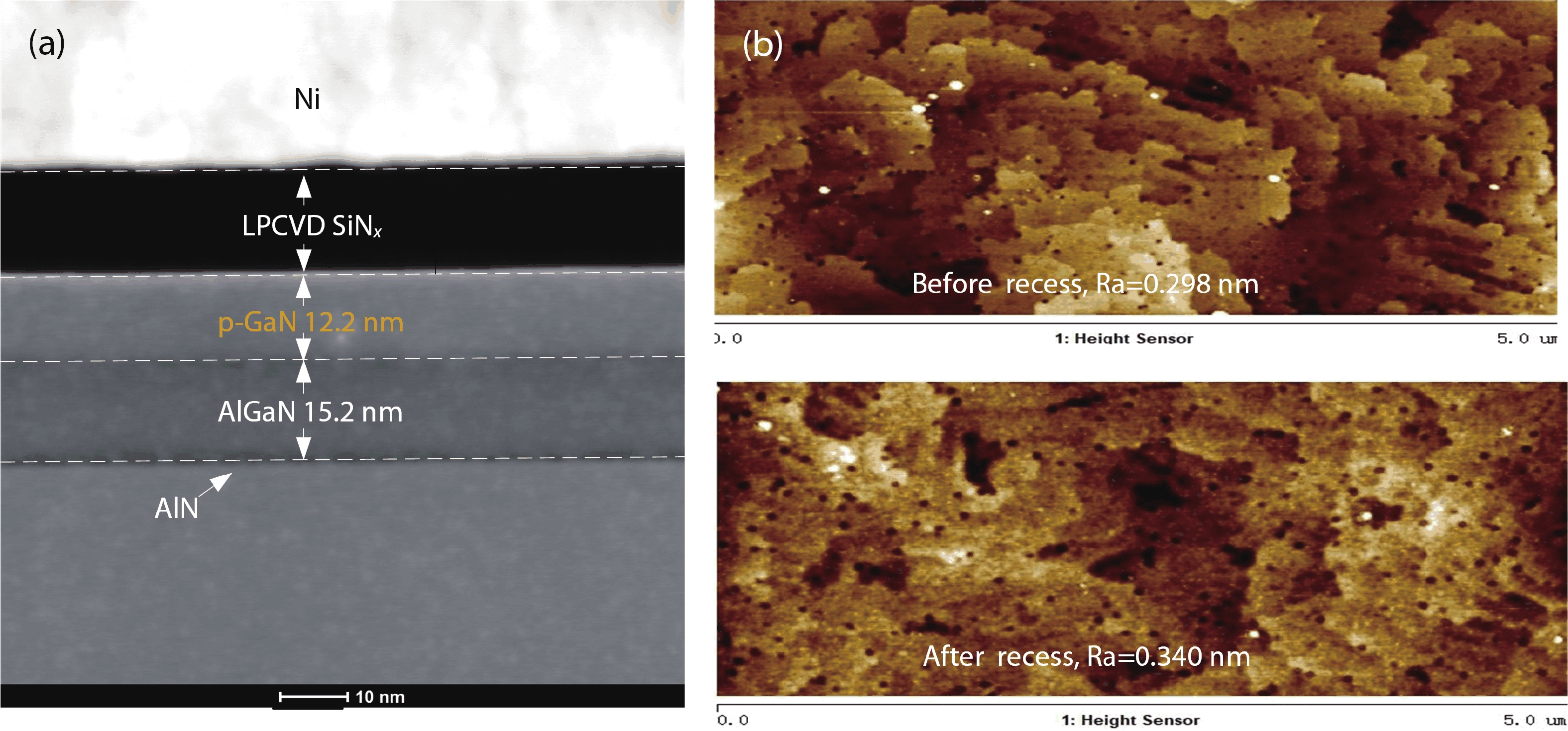
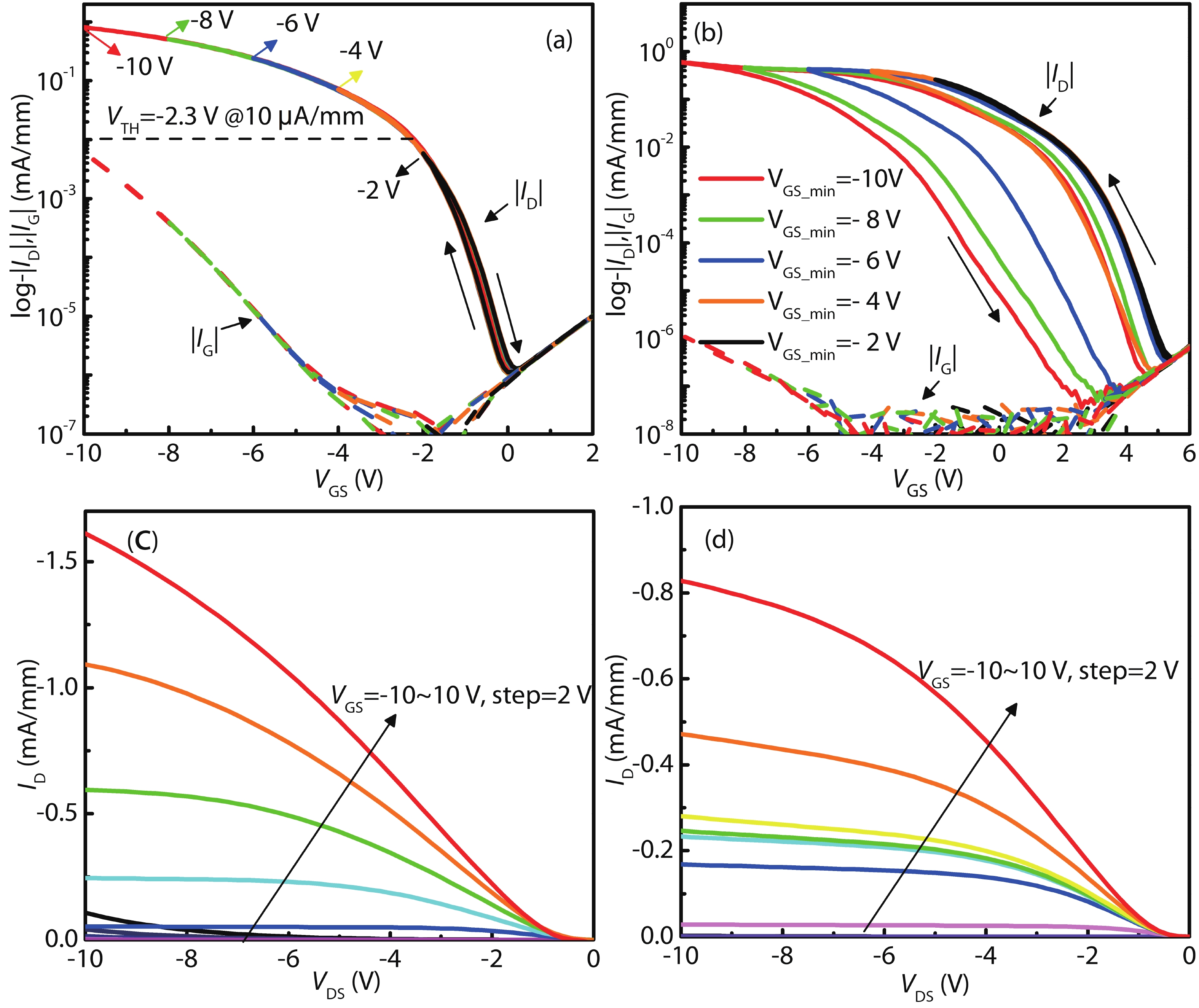
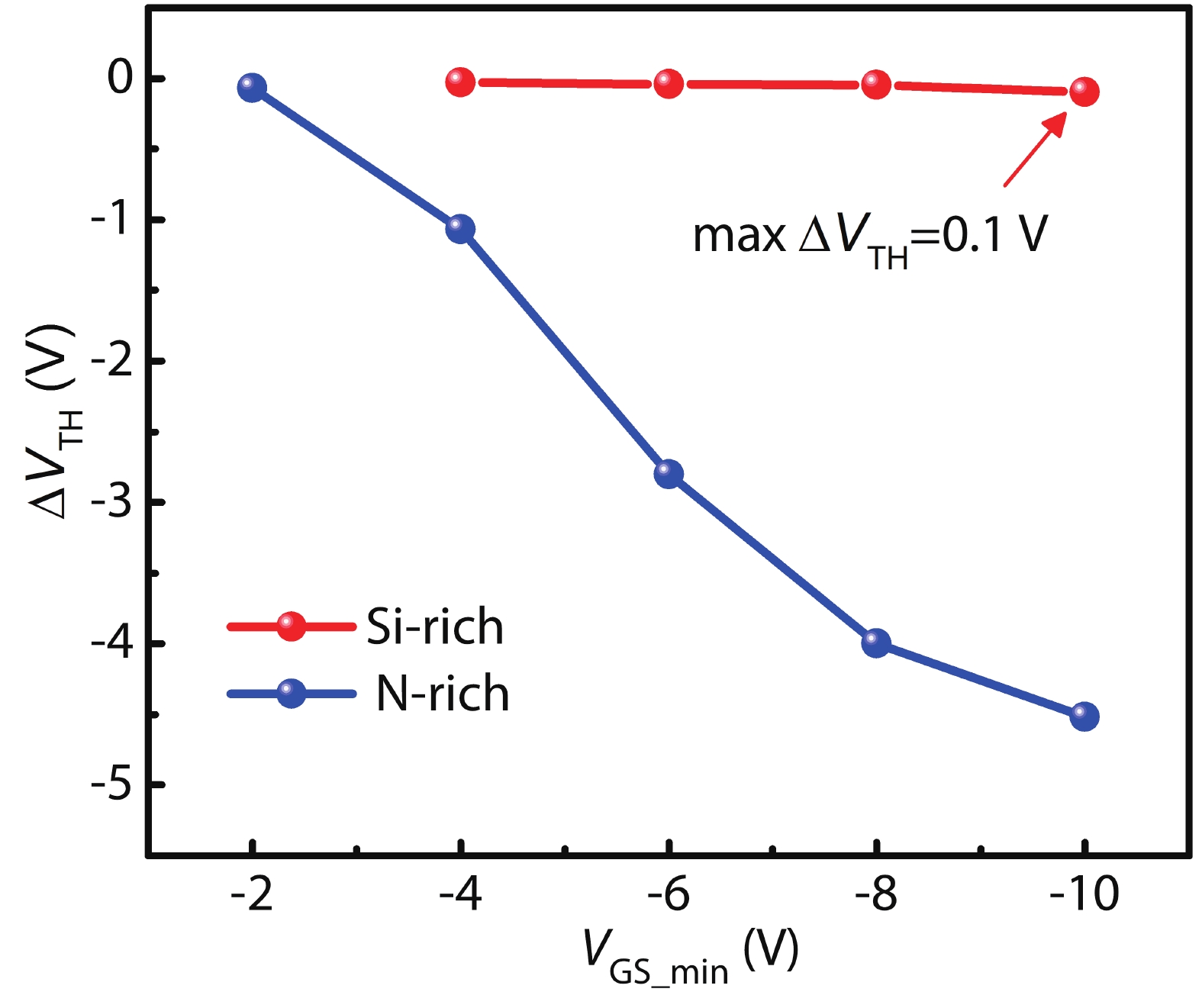
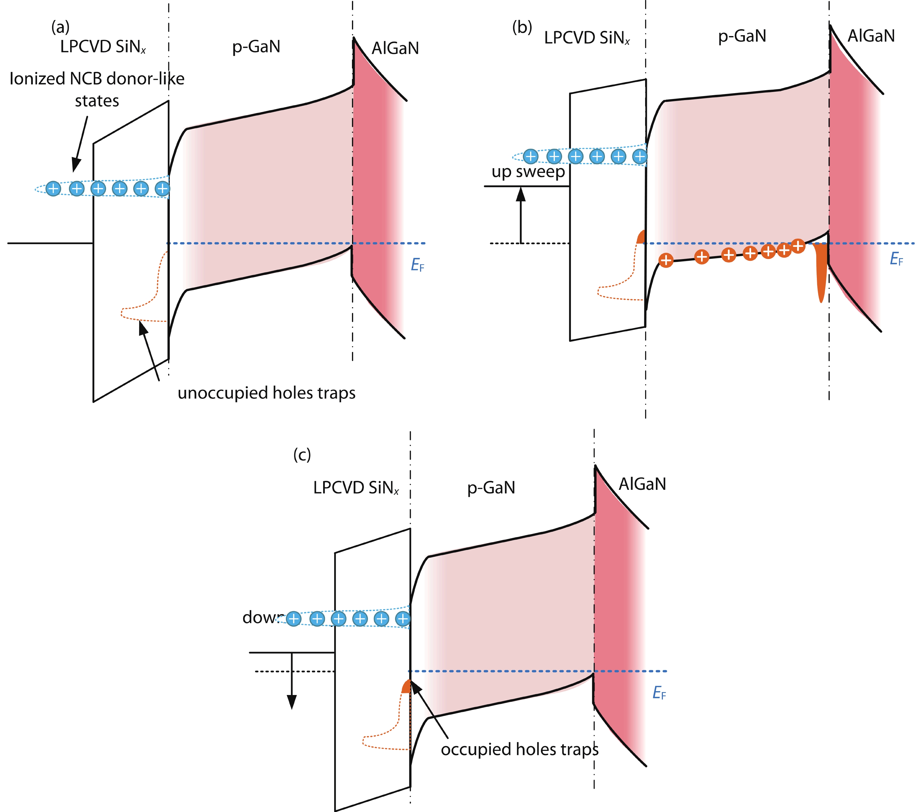
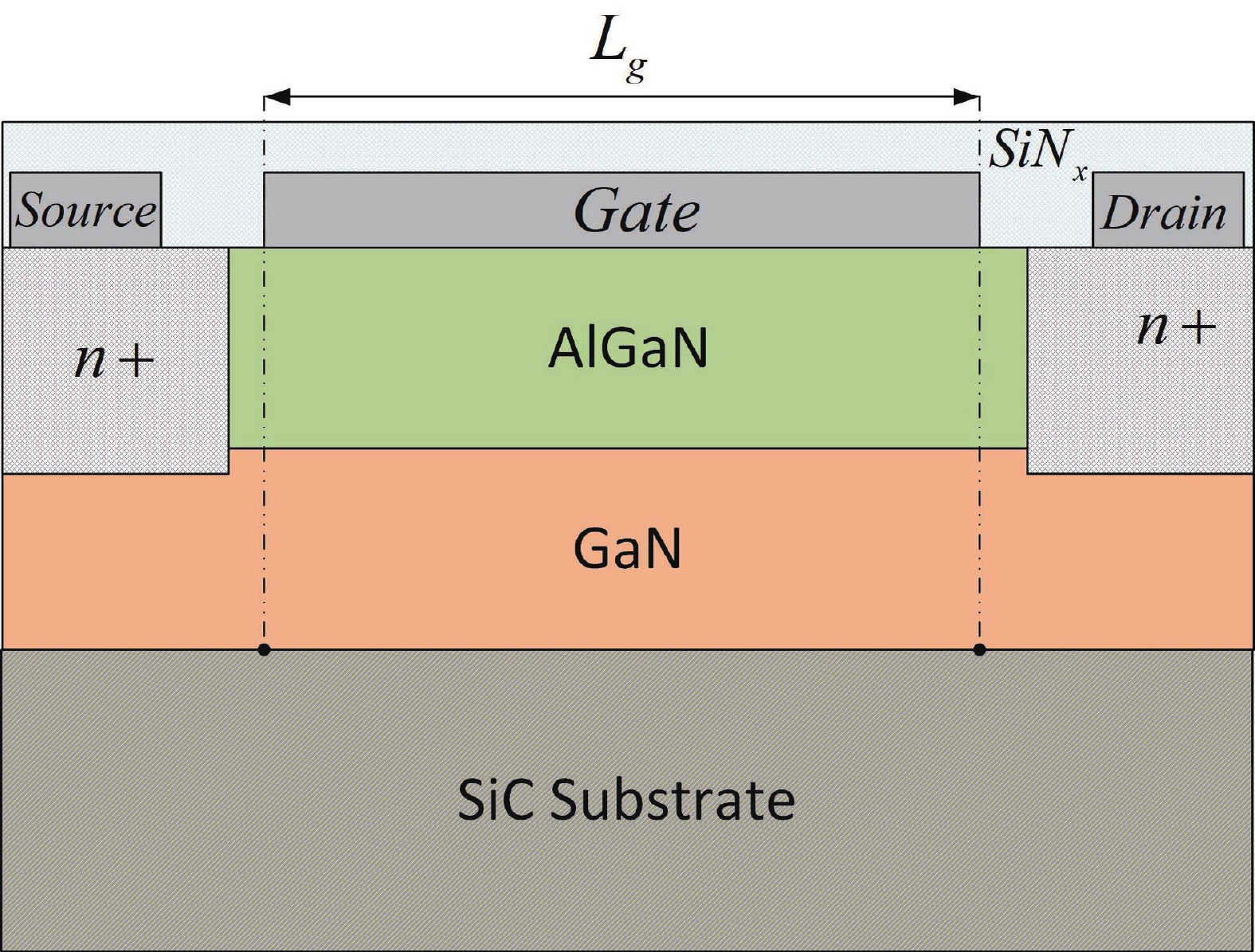
In this work, the GaN p-MISFET with LPCVD-SiNx is studied as a gate dielectric to improve device performance. By changing the Si/N stoichiometry of SiNx, it is found that the channel hole mobility can be effectively enhanced with Si-rich SiNx gate dielectric, which leads to a respectably improved drive current of GaN p-FET. The record high channel mobility of 19.4 cm2/(V∙s) was achieved in the device featuring an Enhancement-mode channel. Benefiting from the significantly improved channel mobility, the fabricated E-mode GaN p-MISFET is capable of delivering a decent-high current of 1.6 mA/mm, while simultaneously featuring a negative threshold-voltage (VTH) of –2.3 V (defining at a stringent criteria of 10 μA/mm). The device also exhibits a well pinch-off at 0 V with low leakage current of 1 nA/mm. This suggests that a decent E-mode operation of the fabricated p-FET is obtained. In addition, the VTH shows excellent stability, while the threshold-voltage hysteresis ΔVTH is as small as 0.1 V for a gate voltage swing up to –10 V, which is among the best results reported in the literature. The results indicate that optimizing the Si/N stoichiometry of LPCVD-SiNx is a promising approach to improve the device performance of GaN p-MISFET.


J. Semicond.
2023, 44(8): 082802 doi: 10.1088/1674-4926/44/8/082802
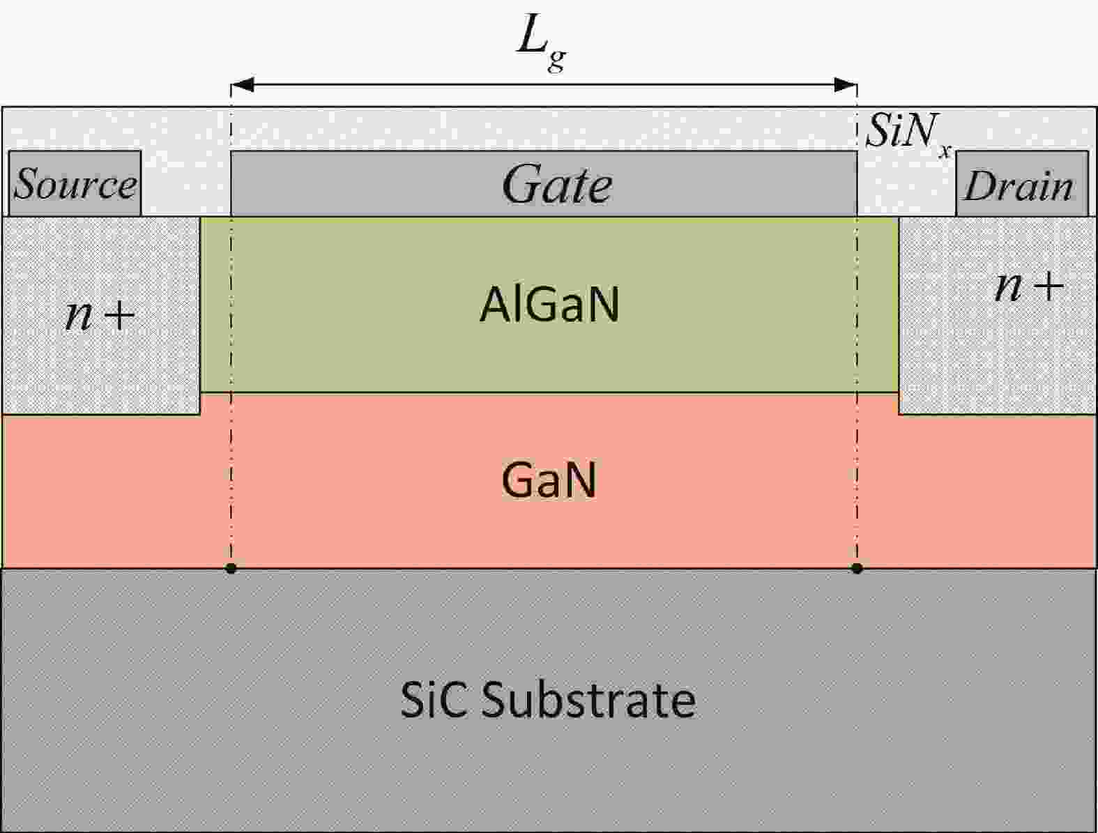
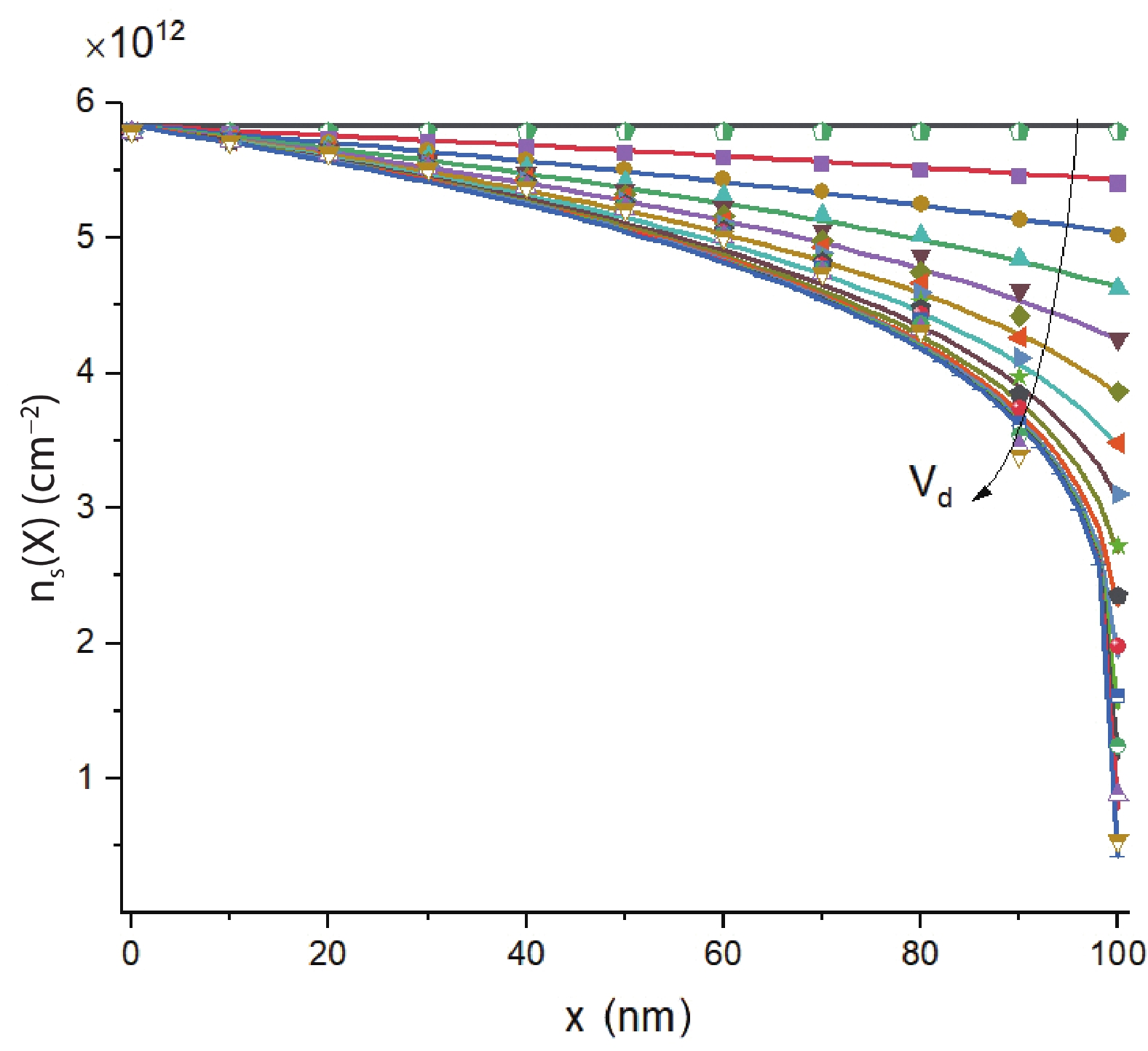
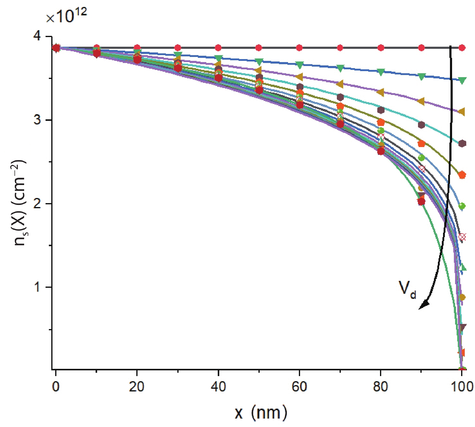
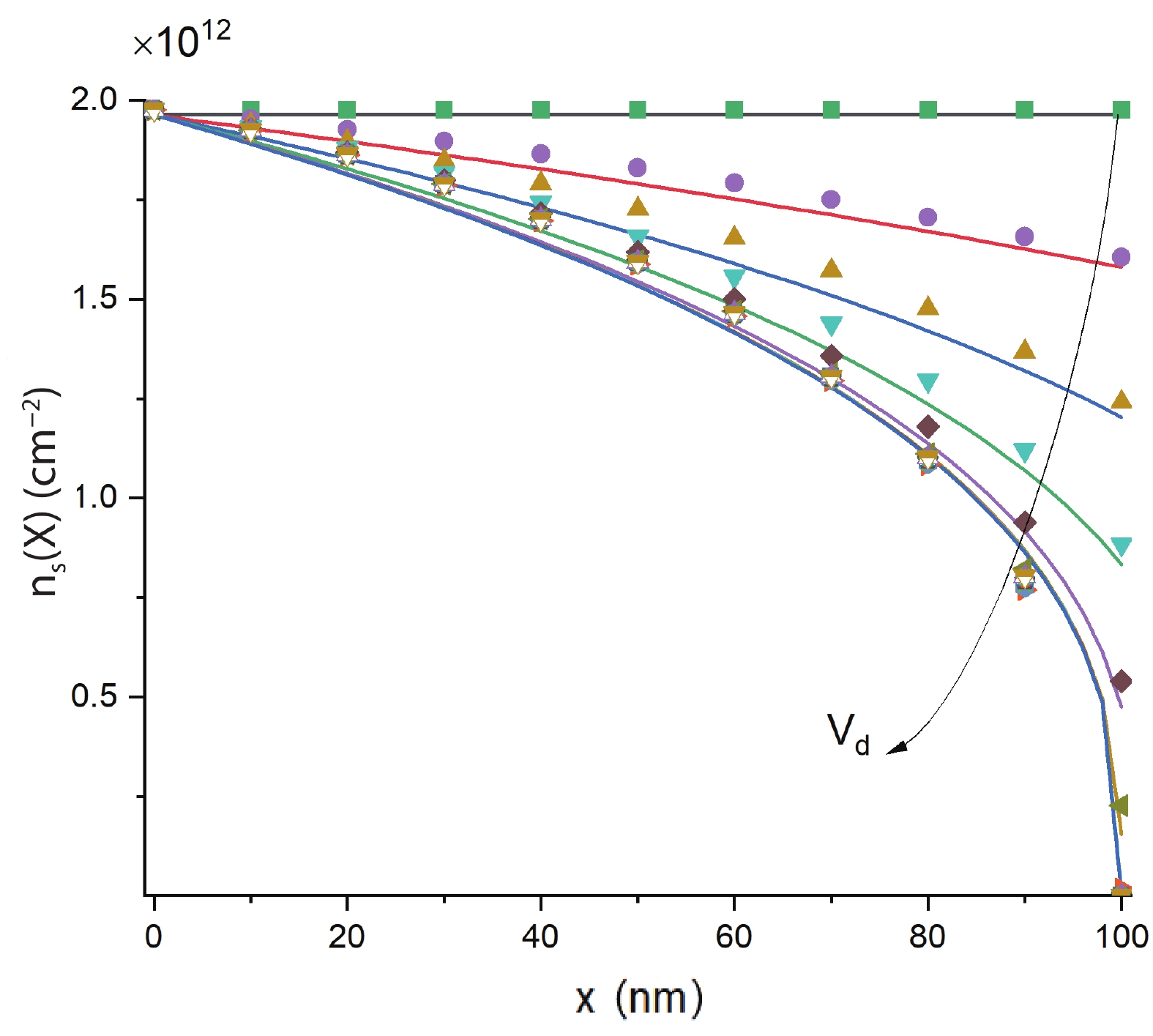
A physics-based analytical expression that predicts the charge, electrical field and potential distributions along the gated region of the GaN HEMT channel has been developed. Unlike the gradual channel approximation (GCA), the proposed model considers the non-uniform variation of the concentration under the gated region as a function of terminal applied voltages. In addition, the model can capture the influence of mobility and channel temperature on the charge distribution trend. The comparison with the hydrodynamic (HD) numerical simulation showed a high agreement of the proposed model with numerical data for different bias conditions considering the self-heating and quantization of the electron concentration. The analytical nature of the model allows us to reduce the computational and time cost of the simulation. Also, it can be used as a core expression to develop a complete physics-based transistor Ⅳ model without GCA limitation.
J. Semicond.
2023, 44(8): 082901 doi: 10.1088/1674-4926/44/8/082901
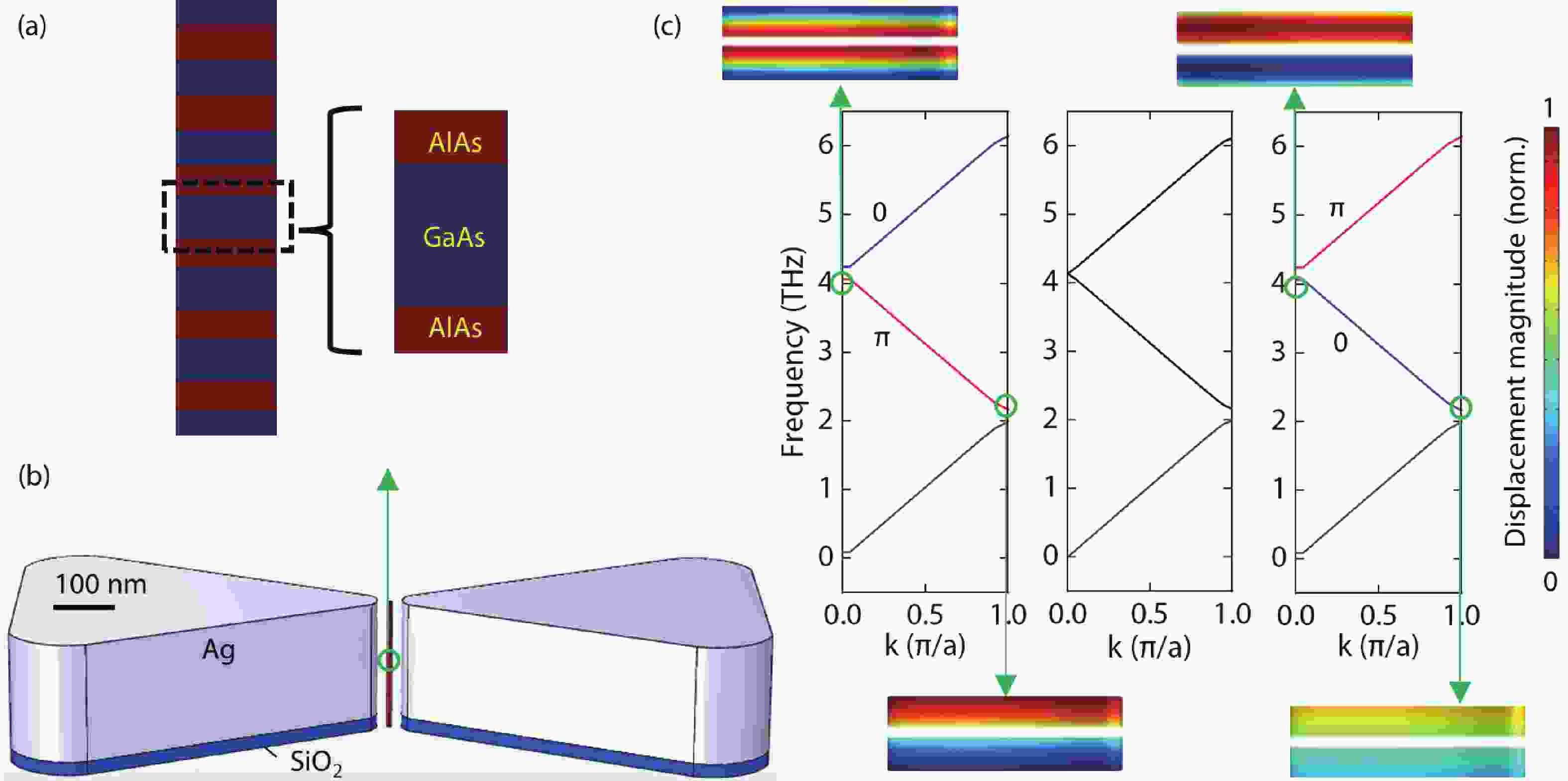
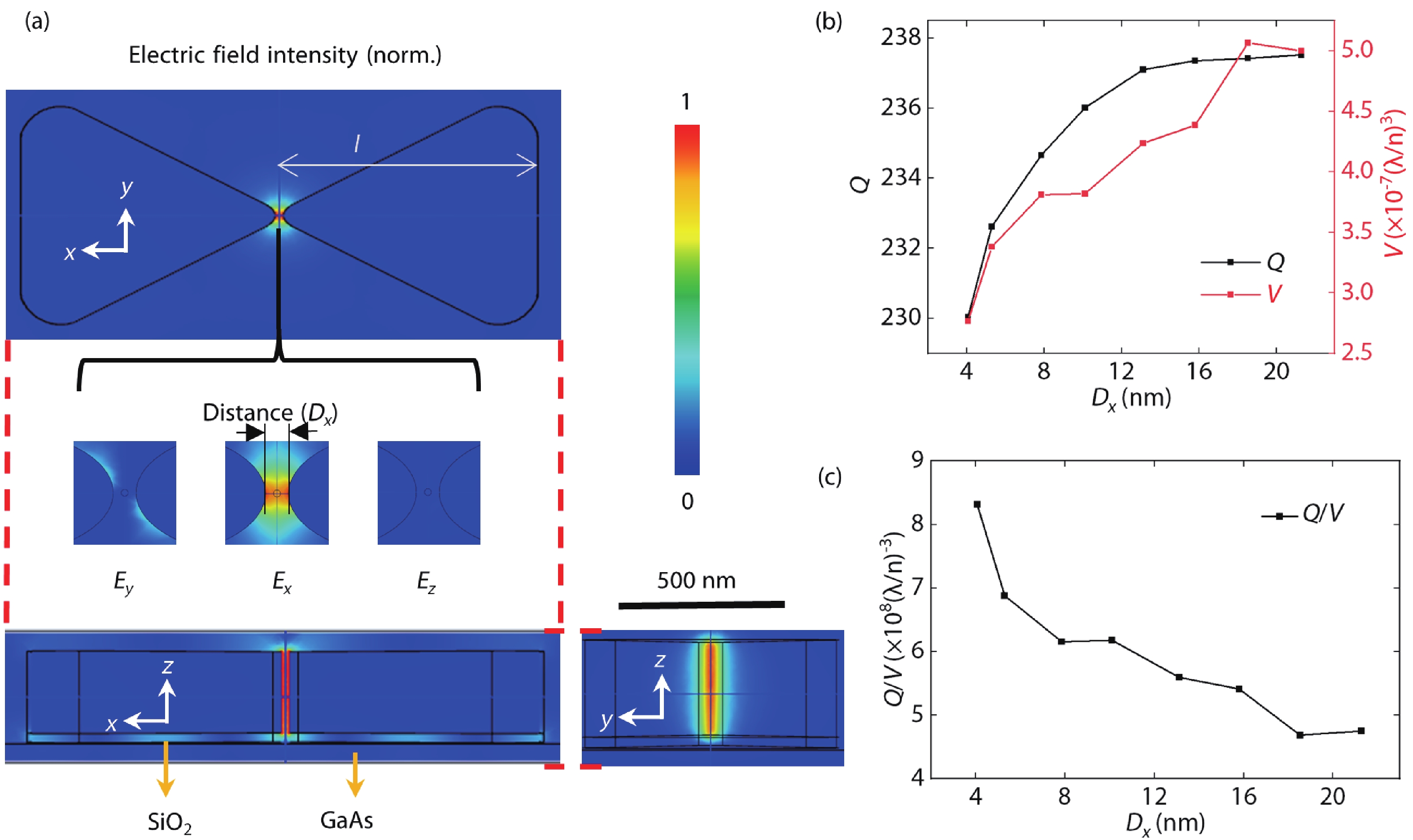
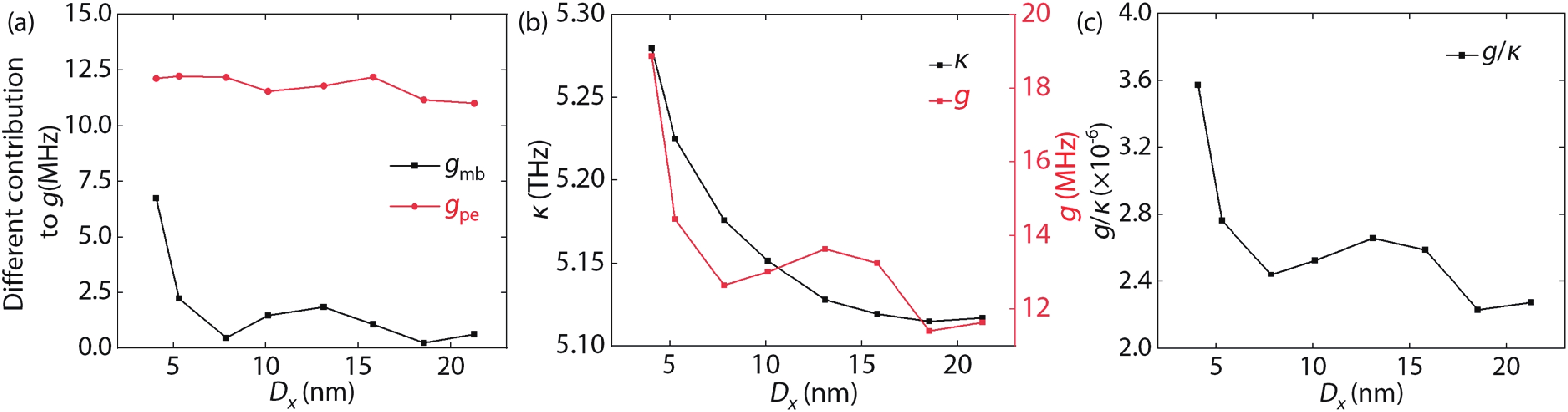
Interaction between photons and phonons in cavity optomechanical systems provides a new toolbox for quantum information technologies. A GaAs/AlAs pillar multi-optical mode microcavity optomechanical structure can obtain phonons with ultra-high frequency (~THz). However, the optical field cannot be effectively restricted when the diameter of the GaAs/AlAs pillar microcavity decreases below the diffraction limit of light. Here, we design a system that combines Ag nanocavity with GaAs/AlAs phononic superlattices, where phonons with the frequency of 4.2 THz can be confined in a pillar with ~4 nm diameter. The Qc/V reaches 0.22 nm−3, which is ~80 times that of the photonic crystal (PhC) nanobeam and ~100 times that of the hybrid point-defect PhC bowtie plasmonic nanocavity, where Qc is optical quality factor and V is mode volume. The optomechanical single-photon coupling strength can reach 12 MHz, which is an order of magnitude larger than that of the PhC nanobeam. In addition, the mechanical zero-point fluctuation amplitude is 85 fm and the efficient mass is 0.27 zg, which is much smaller than the PhC nanobeam. The phononic superlattice-Ag nanocavity optomechanical devices hold great potential for applications in the field of integrated quantum optomechanics, quantum information, and terahertz-light transducer.