


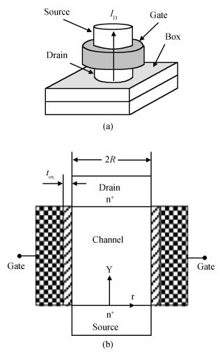
Fig. 1.
(a) Structure and (b) cross section of cylindrical SG MOSFETs.
SEMICONDUCTOR DEVICES
Abstract: An analytical model for surrounding gate metal-oxide-semiconductor field effect transistors (MOSFETs) considering quantum effects is presented. To achieve this goal, we have used a variational approach for solving the Poission and Schrodinger equations. This model is developed to provide an analytical expression for the inversion charge distribution function for all regions of the device operation. This expression is used to calculate the other important parameters like the inversion charge centroid, threshold voltage and inversion charge density. The calculated expressions for the above parameters are simple and accurate. The validity of this model was checked for the devices with different device dimensions and bias voltages. The calculated results are compared with the simulation results and they show good agreement.
Key words: surrounding gate MOSFETs, energy quantization, centroid, inversion charge density
| [1] |
Bendib T, Djeffal F. Electrical performance optimization of nanoscale double-gate MOSFETs using multi-objective genetic algorithms. IEEE Trans Electron Devices, 2011, 58:3743 doi: 10.1109/TED.2011.2163820
|
| [2] |
Bentrcia T, Djeffal F, Benhaya A. Continuous analytic IV model for GS DG MOSFETs including hot-carrier degradation effects. Journal of Semiconductors, 2012, 33:014001 doi: 10.1088/1674-4926/33/1/014001
|
| [3] |
El Hamid H A, Iiguez B, Guitart J R. Analytical model of the threshold voltage and subthreshold swing of undoped cylindrical gate all around based MOSFETs. IEEE Trans Electron Devices, 2007, 54(3):572 doi: 10.1109/TED.2006.890595
|
| [4] |
He J, Liu F, Bian W, et al. An approximate carrier-based compact model for fully depleted surrounding-gate MOSFETs with a finite doping body. Semicond Sci Technol, 2007, 22(6):671 doi: 10.1088/0268-1242/22/6/015
|
| [5] |
Son A, Kim J, Jeong N, et al. Improved explicit current-voltage model for long-channel undoped surrounding-gate metal oxide semiconductor field effect transistor. J Appl Phys, 2009, 48:412 doi: 10.1007/s10825-016-0817-2
|
| [6] |
Chen Y, Luo J. A comparative study of double-gate and surrounding-gate MOSFETs in strong inversion and accumulation using an analytical model. Proc Int Conf Modeling Simulation of Microsystems, 2001, 1:546 http://citeseerx.ist.psu.edu/viewdoc/summary?doi=10.1.1.517.6025
|
| [7] |
Jimenez D, Inguiez B. Continuous analytic IV model for surrounding-gate MOSFETs. IEEE Electron Device Lett, 2004, 25(8):571 doi: 10.1109/LED.2004.831902
|
| [8] |
Iniguez B, Jimenez D, Roig J, et al. Explicit continuous model for long-channel undoped surrounding-gate MOSFETs. IEEE Trans Electron. Devices, 2005, 52(8):1868 doi: 10.1109/TED.2005.852892
|
| [9] |
Colinge J P. Multiple-gate SOI MOSFETs. Solid-State Electron, 2004, 48:897 doi: 10.1016/j.sse.2003.12.020
|
| [10] |
Stern F, Howard W E. Properties of semiconductor surface inversion layers in the electric quantum limit. Phys Rev, 1967, 163(3):816 doi: 10.1103/PhysRev.163.816
|
| [11] |
Stern F. Self-consistent results for n-type Si inversion layers. Phys Rev B Condens Matter, 1972, 5(12):4891 doi: 10.1103/PhysRevB.5.4891
|
| [12] |
Yuan Y, Yu B, Song J, et al. An Analytical model for threshold voltage shift due to quantum confinment in surrounding gate MOSFETs with anisotropic effective mass. Solid-State Electron, 2009, 53:140 doi: 10.1016/j.sse.2008.10.010
|
| [13] |
Wu Y S, Su P. Analytical quantum-confinement model for short-channel gate-all-around MOSFETs under subthreshold region. IEEE Trans Electron Devices, 2009, 56(11):2720 doi: 10.1109/TED.2009.2030714
|
| [14] |
Moreno E, Roldan J B, Barrera D, et al. An analytical model foe square GAA MOSFETs including quantum effects. Solid-State Electron, 2010, 54:1463 doi: 10.1016/j.sse.2010.05.032
|
| [15] |
Roldan J B, Godoy A, Gamiz F, et al. Modeling the centroid and the inversion charge in cylindrical surrounding gate MOSFETs, including quantum effects. IEEE Trans Electron Devices, 2008, 55(1):411 doi: 10.1109/TED.2007.911096
|
| [16] |
Vimala P, Balamurugan N B. Quantum mechanical compact modeling of symmetric double-gate MOSFETs using variational approach. Journal of Semiconductors, 2012, 33(3):034001 doi: 10.1088/1674-4926/33/3/034001
|
| [17] |
Lopez-Villanueva J A, Catujo-Cassinello P, Gámiz F, et al. Effects of the inversion-layer centroid on the performance of double-gateMOSFET's. IEEE Trans Electron Devices, 2000, 47:141 doi: 10.1109/16.817579
|
| [18] |
Lopez-Villanueva J A, Cartujo-Cassinello P, Banqueri J, et al. Effects of the inversion layer centroid on MOSFET behavior. IEEE Trans Electron Devices, 1997, 44:1915 doi: 10.1109/16.641361
|

Table 1. The values of parameters used in simulations.

|
| [1] |
Bendib T, Djeffal F. Electrical performance optimization of nanoscale double-gate MOSFETs using multi-objective genetic algorithms. IEEE Trans Electron Devices, 2011, 58:3743 doi: 10.1109/TED.2011.2163820
|
| [2] |
Bentrcia T, Djeffal F, Benhaya A. Continuous analytic IV model for GS DG MOSFETs including hot-carrier degradation effects. Journal of Semiconductors, 2012, 33:014001 doi: 10.1088/1674-4926/33/1/014001
|
| [3] |
El Hamid H A, Iiguez B, Guitart J R. Analytical model of the threshold voltage and subthreshold swing of undoped cylindrical gate all around based MOSFETs. IEEE Trans Electron Devices, 2007, 54(3):572 doi: 10.1109/TED.2006.890595
|
| [4] |
He J, Liu F, Bian W, et al. An approximate carrier-based compact model for fully depleted surrounding-gate MOSFETs with a finite doping body. Semicond Sci Technol, 2007, 22(6):671 doi: 10.1088/0268-1242/22/6/015
|
| [5] |
Son A, Kim J, Jeong N, et al. Improved explicit current-voltage model for long-channel undoped surrounding-gate metal oxide semiconductor field effect transistor. J Appl Phys, 2009, 48:412 doi: 10.1007/s10825-016-0817-2
|
| [6] |
Chen Y, Luo J. A comparative study of double-gate and surrounding-gate MOSFETs in strong inversion and accumulation using an analytical model. Proc Int Conf Modeling Simulation of Microsystems, 2001, 1:546 http://citeseerx.ist.psu.edu/viewdoc/summary?doi=10.1.1.517.6025
|
| [7] |
Jimenez D, Inguiez B. Continuous analytic IV model for surrounding-gate MOSFETs. IEEE Electron Device Lett, 2004, 25(8):571 doi: 10.1109/LED.2004.831902
|
| [8] |
Iniguez B, Jimenez D, Roig J, et al. Explicit continuous model for long-channel undoped surrounding-gate MOSFETs. IEEE Trans Electron. Devices, 2005, 52(8):1868 doi: 10.1109/TED.2005.852892
|
| [9] |
Colinge J P. Multiple-gate SOI MOSFETs. Solid-State Electron, 2004, 48:897 doi: 10.1016/j.sse.2003.12.020
|
| [10] |
Stern F, Howard W E. Properties of semiconductor surface inversion layers in the electric quantum limit. Phys Rev, 1967, 163(3):816 doi: 10.1103/PhysRev.163.816
|
| [11] |
Stern F. Self-consistent results for n-type Si inversion layers. Phys Rev B Condens Matter, 1972, 5(12):4891 doi: 10.1103/PhysRevB.5.4891
|
| [12] |
Yuan Y, Yu B, Song J, et al. An Analytical model for threshold voltage shift due to quantum confinment in surrounding gate MOSFETs with anisotropic effective mass. Solid-State Electron, 2009, 53:140 doi: 10.1016/j.sse.2008.10.010
|
| [13] |
Wu Y S, Su P. Analytical quantum-confinement model for short-channel gate-all-around MOSFETs under subthreshold region. IEEE Trans Electron Devices, 2009, 56(11):2720 doi: 10.1109/TED.2009.2030714
|
| [14] |
Moreno E, Roldan J B, Barrera D, et al. An analytical model foe square GAA MOSFETs including quantum effects. Solid-State Electron, 2010, 54:1463 doi: 10.1016/j.sse.2010.05.032
|
| [15] |
Roldan J B, Godoy A, Gamiz F, et al. Modeling the centroid and the inversion charge in cylindrical surrounding gate MOSFETs, including quantum effects. IEEE Trans Electron Devices, 2008, 55(1):411 doi: 10.1109/TED.2007.911096
|
| [16] |
Vimala P, Balamurugan N B. Quantum mechanical compact modeling of symmetric double-gate MOSFETs using variational approach. Journal of Semiconductors, 2012, 33(3):034001 doi: 10.1088/1674-4926/33/3/034001
|
| [17] |
Lopez-Villanueva J A, Catujo-Cassinello P, Gámiz F, et al. Effects of the inversion-layer centroid on the performance of double-gateMOSFET's. IEEE Trans Electron Devices, 2000, 47:141 doi: 10.1109/16.817579
|
| [18] |
Lopez-Villanueva J A, Cartujo-Cassinello P, Banqueri J, et al. Effects of the inversion layer centroid on MOSFET behavior. IEEE Trans Electron Devices, 1997, 44:1915 doi: 10.1109/16.641361
|


Article views: 2023 Times PDF downloads: 29 Times Cited by: 0 Times
Received: 13 May 2013 Revised: 06 June 2013 Online: Published: 01 November 2013
| Citation: |
P. Vimala, N. B. Balamurugan. Modeling and simulation of centroid and inversion charge density in cylindrical surrounding gate MOSFETs including quantum effects[J]. Journal of Semiconductors, 2013, 34(11): 114001. doi: 10.1088/1674-4926/34/11/114001
P Vimala, N B Balamurugan. Modeling and simulation of centroid and inversion charge density in cylindrical surrounding gate MOSFETs including quantum effects[J]. J. Semicond., 2013, 34(11): 114001. doi: 10.1088/1674-4926/34/11/114001.
Export: BibTex EndNote

|
| [1] |
Bendib T, Djeffal F. Electrical performance optimization of nanoscale double-gate MOSFETs using multi-objective genetic algorithms. IEEE Trans Electron Devices, 2011, 58:3743 doi: 10.1109/TED.2011.2163820
|
| [2] |
Bentrcia T, Djeffal F, Benhaya A. Continuous analytic IV model for GS DG MOSFETs including hot-carrier degradation effects. Journal of Semiconductors, 2012, 33:014001 doi: 10.1088/1674-4926/33/1/014001
|
| [3] |
El Hamid H A, Iiguez B, Guitart J R. Analytical model of the threshold voltage and subthreshold swing of undoped cylindrical gate all around based MOSFETs. IEEE Trans Electron Devices, 2007, 54(3):572 doi: 10.1109/TED.2006.890595
|
| [4] |
He J, Liu F, Bian W, et al. An approximate carrier-based compact model for fully depleted surrounding-gate MOSFETs with a finite doping body. Semicond Sci Technol, 2007, 22(6):671 doi: 10.1088/0268-1242/22/6/015
|
| [5] |
Son A, Kim J, Jeong N, et al. Improved explicit current-voltage model for long-channel undoped surrounding-gate metal oxide semiconductor field effect transistor. J Appl Phys, 2009, 48:412 doi: 10.1007/s10825-016-0817-2
|
| [6] |
Chen Y, Luo J. A comparative study of double-gate and surrounding-gate MOSFETs in strong inversion and accumulation using an analytical model. Proc Int Conf Modeling Simulation of Microsystems, 2001, 1:546 http://citeseerx.ist.psu.edu/viewdoc/summary?doi=10.1.1.517.6025
|
| [7] |
Jimenez D, Inguiez B. Continuous analytic IV model for surrounding-gate MOSFETs. IEEE Electron Device Lett, 2004, 25(8):571 doi: 10.1109/LED.2004.831902
|
| [8] |
Iniguez B, Jimenez D, Roig J, et al. Explicit continuous model for long-channel undoped surrounding-gate MOSFETs. IEEE Trans Electron. Devices, 2005, 52(8):1868 doi: 10.1109/TED.2005.852892
|
| [9] |
Colinge J P. Multiple-gate SOI MOSFETs. Solid-State Electron, 2004, 48:897 doi: 10.1016/j.sse.2003.12.020
|
| [10] |
Stern F, Howard W E. Properties of semiconductor surface inversion layers in the electric quantum limit. Phys Rev, 1967, 163(3):816 doi: 10.1103/PhysRev.163.816
|
| [11] |
Stern F. Self-consistent results for n-type Si inversion layers. Phys Rev B Condens Matter, 1972, 5(12):4891 doi: 10.1103/PhysRevB.5.4891
|
| [12] |
Yuan Y, Yu B, Song J, et al. An Analytical model for threshold voltage shift due to quantum confinment in surrounding gate MOSFETs with anisotropic effective mass. Solid-State Electron, 2009, 53:140 doi: 10.1016/j.sse.2008.10.010
|
| [13] |
Wu Y S, Su P. Analytical quantum-confinement model for short-channel gate-all-around MOSFETs under subthreshold region. IEEE Trans Electron Devices, 2009, 56(11):2720 doi: 10.1109/TED.2009.2030714
|
| [14] |
Moreno E, Roldan J B, Barrera D, et al. An analytical model foe square GAA MOSFETs including quantum effects. Solid-State Electron, 2010, 54:1463 doi: 10.1016/j.sse.2010.05.032
|
| [15] |
Roldan J B, Godoy A, Gamiz F, et al. Modeling the centroid and the inversion charge in cylindrical surrounding gate MOSFETs, including quantum effects. IEEE Trans Electron Devices, 2008, 55(1):411 doi: 10.1109/TED.2007.911096
|
| [16] |
Vimala P, Balamurugan N B. Quantum mechanical compact modeling of symmetric double-gate MOSFETs using variational approach. Journal of Semiconductors, 2012, 33(3):034001 doi: 10.1088/1674-4926/33/3/034001
|
| [17] |
Lopez-Villanueva J A, Catujo-Cassinello P, Gámiz F, et al. Effects of the inversion-layer centroid on the performance of double-gateMOSFET's. IEEE Trans Electron Devices, 2000, 47:141 doi: 10.1109/16.817579
|
| [18] |
Lopez-Villanueva J A, Cartujo-Cassinello P, Banqueri J, et al. Effects of the inversion layer centroid on MOSFET behavior. IEEE Trans Electron Devices, 1997, 44:1915 doi: 10.1109/16.641361
|

 WeChat ID
Journal of Semiconductors © 2017 All Rights Reserved 京ICP备05085259号-2

 DownLoad:

