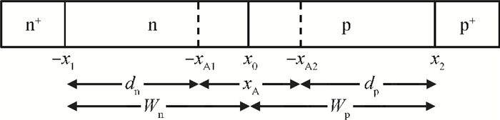
Fig. 1.
One-dimensional model of the DDR IMPATT device.
SEMICONDUCTOR DEVICES
Abstract: The authors have developed a large-signal simulation technique extending an in-house small-signal simulation code for analyzing a 94 GHz double-drift region impact avalanche transit time device based on silicon with a non-sinusoidal voltage excitation and studied the effect of junction temperature between 300 and 550 K on the large-signal characteristics of the device for both continuous wave (CW) and pulsed modes of operation. Results show that the large-signal RF power output of the device in both CW and pulsed modes increases with the increase of voltage modulation factor up to 60%, but decreases sharply with further increase of voltage modulation factor for a particular junction temperature; while the same parameter increases with the increase of junction temperature for a particular voltage modulation factor. Heat sinks made of copper and type-ⅡA diamond are designed to carry out the steady-state and transient thermal analysis of the device operating in CW and pulsed modes respectively. Authors have adopted Olson's method to carry out the transient analysis of the device, which clearly establishes the superiority of type-ⅡA diamond over copper as the heat sink material of the device from the standpoint of the undesirable effect of frequency chirping due to thermal transients in the pulsed mode.
Key words: admittance characteristics, chirp bandwidth, frequency chirping, junction temperature, large-signal analysis, transient thermal analysis
| [1] |
Midford T A, Bernick R L. Millimeter wave CW IMPATT diodes and oscillators. IEEE Trans Microw Theory Tech, 1979, 27:483 doi: 10.1109/TMTT.1979.1129653
|
| [2] |
Chang Y, Hellum J M, Paul J A, et al. Millimeter-wave IMPATT sources for communication applications. IEEE MTT-S International Microwave Symposium Digest, 1977:216
|
| [3] |
Gray W W, Kikushima L, Morentc N P, et al. Applying IMPATT power sources to modern microwave systems. IEEE J Solid-State Circuits, 1969, 4:409 doi: 10.1109/JSSC.1969.1050046
|
| [4] |
Miswa T. Negative resistance in p-n junctions under avalanche breakdown conditions. IEEE Trans Electron Devices, 1966, 33:137
|
| [5] |
Gilden M, Hines M E. Electronic tuning effects in the read microwave avalanche diode. IEEE Trans Electron Devices, 1966, 13(1):169 http://ieeexplore.ieee.org/document/1474242/
|
| [6] |
Gummel H K, Scharfetter D L. Avalanche region of IMPATT diodes. Bell Sys Tech J, 1966, 45:1797 doi: 10.1002/bltj.1966.45.issue-10
|
| [7] |
Evans W J, Haddad G I. A large-signal analysis of IMPATT diodes. IEEE Trans Electron Devices, 1968, 15(10):708 doi: 10.1109/T-ED.1968.16503
|
| [8] |
Scharfetter D L, Gummel H K. Large-signal analysis of a silicon read diode oscillator. IEEE Trans Electron Devices, 1969, 6(1):64 http://ieeexplore.ieee.org/document/1475609/
|
| [9] |
Gupta M S, Lomax R J. A current-excited large-signal analysis of IMPATT devices and its circuit implementations. IEEE Trans Electron Devices, 1973, 20:395 doi: 10.1109/T-ED.1973.17661
|
| [10] |
Roy S K, Sridharan M, Ghosh R, et al. Computer method for the dc field and carrier current profiles in the IMPATT device starting from the field extremum in the depletion layer. In:Miller J H, ed. Proceedings of the 1st Conference on Numerical Analysis of Semiconductor Devices (NASECODE I), Dublin, Ireland, 1979:266
|
| [11] |
Roy S K, Banerjee J P, Pati S P. A computer analysis of the distribution of high frequency negative resistance in the depletion layer of IMPATT diodes. Proceedings of 4th Conf on Num Anal of Semiconductor Devices (NASECODE IV), Dublin, 1985:494
|
| [12] |
Gummel H K, Blue J L. A small-signal theory of avalanche noise in IMPATT diodes. IEEE Trans Electron Devices, 1967, 14(9):569 doi: 10.1109/T-ED.1967.16005
|
| [13] |
Sze S M, Ryder R M. Microwave avalanche diodes. Proc IEEE, Special Issue on Microwave Semiconductor Devices, 1971, 59(8):1140 http://ieeexplore.ieee.org/abstract/document/1450290/
|
| [14] |
Grant W N. Electron and hole ionization rates in epitaxial silicon. Solid-State Electron, 1973, 16(10):1189 doi: 10.1016/0038-1101(73)90147-0
|
| [15] |
Canali C, Ottaviani G, Quaranta A A. Drift velocity of electrons and holes and associated anisotropic effects in silicon. J Phys Chem Solids, 1971, 32(8):1707 doi: 10.1016/S0022-3697(71)80137-3
|
| [16] |
Zeghbroeck B V. Principles of semiconductor devices. Colorado Press, 2011 http://ci.nii.ac.jp/ncid/BB0860083X
|
| [17] |
"Electronic Archive: New Semiconductor Materials, Characteristics and Properties", http://www.ioffe.ru/SVA/NSM/Semicond/Si/index.html
|
| [18] |
Sridharan M, Roy S K. Computer studies on the widening of the avalanche zone and decrease on efficiency in silicon X-band symmetrical DDR. Electron Lett, 1978, 14:635 doi: 10.1049/el:19780427
|
| [19] |
Sridharan M, Roy S K. Effect of mobile space charge on the small signal admittance of silicon DDR. Solid-State Electron, 1980, 23:1001 doi: 10.1016/0038-1101(80)90070-2
|
| [20] |
Luy J F, Casel A, Behr W, et al. A 90-GHz double-drift IMPATT diode made with Si MBE. IEEE Trans Electron Devices, 1987, 34:1084 doi: 10.1109/T-ED.1987.23049
|
| [21] |
Dalle C, Rolland P, Lieti G. Flat doping profile double-drift silicon IMPATT for reliable CW high power high-efficiency generation in the 94-GHz window. IEEE Trans Electron Devices, 1990, 37:227 doi: 10.1109/16.43820
|
| [22] |
Chang K, Sun C, English D L, et al. High power 94-GHz pulsed IMPATT oscillators. IEEE MTT-S International Microwave Symposium Digest, 1979:71 https://www.infona.pl/resource/bwmeta1.element.ieee-art-000001123974
|
| [23] |
Acharyya A, Mukherjee J, Mukherjee M, et al. Heat sink design for IMPATT diode sources with different base materials operating at 94 GHz. Archives of Physics Research, 2011, 2(1):107
|
| [24] |
Acharyya A, Pal B, Banerjee J P. Temperature distribution inside semi-infinite heat sinks for IMPATT sources. International Journal of Engineering Science and Technology, 2010, 2(10):5142
|
| [25] |
Fong T T, Kuno H J. Millimeter-wave pulsed IMPATT sources. IEEE Trans MTT, 1979, 15(5):492 http://ieeexplore.ieee.org/document/1129654/keywords
|
| [26] |
Olson H M. A mechanism for catastropic failure of Avalanche diodes. IEEE Trans Electron Devices, 1975, 22:842 doi: 10.1109/T-ED.1975.18232
|
| [27] |
Olson H M. Temperature transients in IMPATT diodes. IEEE Trans Electron Devices, 1976, 23(5):494 doi: 10.1109/T-ED.1976.18435
|


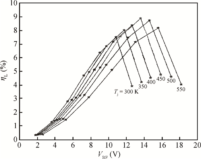
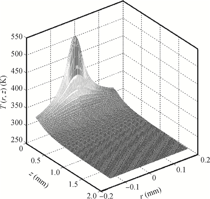
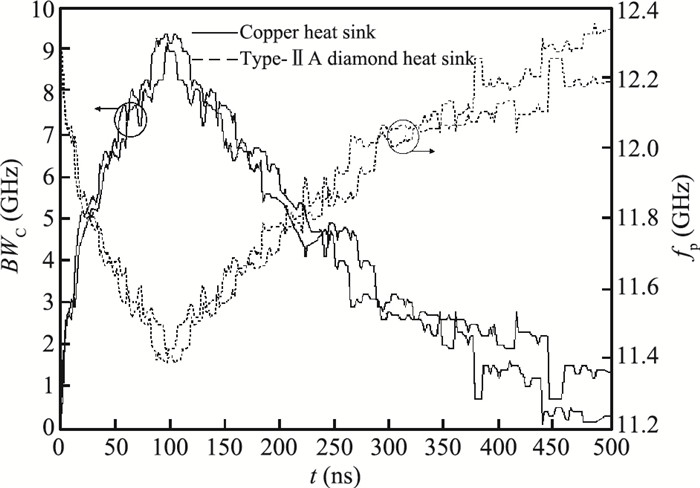
Table 1. Design parameters.

|
Table 2. Static parameters for different junction temperatures.

|
Table 3. Large-signal parameters for different voltage modulation factors at different junction temperatures.

|
Table 4. Heat sink dimensions, thermal resistance and steady-state junction temperatures for the CW mode.

|
Table 5. Heat sink dimensions, thermal resistances and maximum junction temperature for pulsed mode.

|
Table 6. Heat sink dimensions, thermal resistances and maximum junction temperature for pulsed mode.

|
| [1] |
Midford T A, Bernick R L. Millimeter wave CW IMPATT diodes and oscillators. IEEE Trans Microw Theory Tech, 1979, 27:483 doi: 10.1109/TMTT.1979.1129653
|
| [2] |
Chang Y, Hellum J M, Paul J A, et al. Millimeter-wave IMPATT sources for communication applications. IEEE MTT-S International Microwave Symposium Digest, 1977:216
|
| [3] |
Gray W W, Kikushima L, Morentc N P, et al. Applying IMPATT power sources to modern microwave systems. IEEE J Solid-State Circuits, 1969, 4:409 doi: 10.1109/JSSC.1969.1050046
|
| [4] |
Miswa T. Negative resistance in p-n junctions under avalanche breakdown conditions. IEEE Trans Electron Devices, 1966, 33:137
|
| [5] |
Gilden M, Hines M E. Electronic tuning effects in the read microwave avalanche diode. IEEE Trans Electron Devices, 1966, 13(1):169 http://ieeexplore.ieee.org/document/1474242/
|
| [6] |
Gummel H K, Scharfetter D L. Avalanche region of IMPATT diodes. Bell Sys Tech J, 1966, 45:1797 doi: 10.1002/bltj.1966.45.issue-10
|
| [7] |
Evans W J, Haddad G I. A large-signal analysis of IMPATT diodes. IEEE Trans Electron Devices, 1968, 15(10):708 doi: 10.1109/T-ED.1968.16503
|
| [8] |
Scharfetter D L, Gummel H K. Large-signal analysis of a silicon read diode oscillator. IEEE Trans Electron Devices, 1969, 6(1):64 http://ieeexplore.ieee.org/document/1475609/
|
| [9] |
Gupta M S, Lomax R J. A current-excited large-signal analysis of IMPATT devices and its circuit implementations. IEEE Trans Electron Devices, 1973, 20:395 doi: 10.1109/T-ED.1973.17661
|
| [10] |
Roy S K, Sridharan M, Ghosh R, et al. Computer method for the dc field and carrier current profiles in the IMPATT device starting from the field extremum in the depletion layer. In:Miller J H, ed. Proceedings of the 1st Conference on Numerical Analysis of Semiconductor Devices (NASECODE I), Dublin, Ireland, 1979:266
|
| [11] |
Roy S K, Banerjee J P, Pati S P. A computer analysis of the distribution of high frequency negative resistance in the depletion layer of IMPATT diodes. Proceedings of 4th Conf on Num Anal of Semiconductor Devices (NASECODE IV), Dublin, 1985:494
|
| [12] |
Gummel H K, Blue J L. A small-signal theory of avalanche noise in IMPATT diodes. IEEE Trans Electron Devices, 1967, 14(9):569 doi: 10.1109/T-ED.1967.16005
|
| [13] |
Sze S M, Ryder R M. Microwave avalanche diodes. Proc IEEE, Special Issue on Microwave Semiconductor Devices, 1971, 59(8):1140 http://ieeexplore.ieee.org/abstract/document/1450290/
|
| [14] |
Grant W N. Electron and hole ionization rates in epitaxial silicon. Solid-State Electron, 1973, 16(10):1189 doi: 10.1016/0038-1101(73)90147-0
|
| [15] |
Canali C, Ottaviani G, Quaranta A A. Drift velocity of electrons and holes and associated anisotropic effects in silicon. J Phys Chem Solids, 1971, 32(8):1707 doi: 10.1016/S0022-3697(71)80137-3
|
| [16] |
Zeghbroeck B V. Principles of semiconductor devices. Colorado Press, 2011 http://ci.nii.ac.jp/ncid/BB0860083X
|
| [17] |
"Electronic Archive: New Semiconductor Materials, Characteristics and Properties", http://www.ioffe.ru/SVA/NSM/Semicond/Si/index.html
|
| [18] |
Sridharan M, Roy S K. Computer studies on the widening of the avalanche zone and decrease on efficiency in silicon X-band symmetrical DDR. Electron Lett, 1978, 14:635 doi: 10.1049/el:19780427
|
| [19] |
Sridharan M, Roy S K. Effect of mobile space charge on the small signal admittance of silicon DDR. Solid-State Electron, 1980, 23:1001 doi: 10.1016/0038-1101(80)90070-2
|
| [20] |
Luy J F, Casel A, Behr W, et al. A 90-GHz double-drift IMPATT diode made with Si MBE. IEEE Trans Electron Devices, 1987, 34:1084 doi: 10.1109/T-ED.1987.23049
|
| [21] |
Dalle C, Rolland P, Lieti G. Flat doping profile double-drift silicon IMPATT for reliable CW high power high-efficiency generation in the 94-GHz window. IEEE Trans Electron Devices, 1990, 37:227 doi: 10.1109/16.43820
|
| [22] |
Chang K, Sun C, English D L, et al. High power 94-GHz pulsed IMPATT oscillators. IEEE MTT-S International Microwave Symposium Digest, 1979:71 https://www.infona.pl/resource/bwmeta1.element.ieee-art-000001123974
|
| [23] |
Acharyya A, Mukherjee J, Mukherjee M, et al. Heat sink design for IMPATT diode sources with different base materials operating at 94 GHz. Archives of Physics Research, 2011, 2(1):107
|
| [24] |
Acharyya A, Pal B, Banerjee J P. Temperature distribution inside semi-infinite heat sinks for IMPATT sources. International Journal of Engineering Science and Technology, 2010, 2(10):5142
|
| [25] |
Fong T T, Kuno H J. Millimeter-wave pulsed IMPATT sources. IEEE Trans MTT, 1979, 15(5):492 http://ieeexplore.ieee.org/document/1129654/keywords
|
| [26] |
Olson H M. A mechanism for catastropic failure of Avalanche diodes. IEEE Trans Electron Devices, 1975, 22:842 doi: 10.1109/T-ED.1975.18232
|
| [27] |
Olson H M. Temperature transients in IMPATT diodes. IEEE Trans Electron Devices, 1976, 23(5):494 doi: 10.1109/T-ED.1976.18435
|


Article views: 2726 Times PDF downloads: 13 Times Cited by: 0 Times
Received: 02 August 2012 Revised: 04 September 2012 Online: Published: 01 February 2013
| Citation: |
Aritra Acharyya, Suranjana Banerjee, J. P. Banerjee. Effect of junction temperature on the large-signal properties of a 94 GHz silicon based double-drift region impact avalanche transit time device[J]. Journal of Semiconductors, 2013, 34(2): 024001. doi: 10.1088/1674-4926/34/2/024001
****
A Acharyya, S Banerjee, J. P. Banerjee. Effect of junction temperature on the large-signal properties of a 94 GHz silicon based double-drift region impact avalanche transit time device[J]. J. Semicond., 2013, 34(2): 024001. doi: 10.1088/1674-4926/34/2/024001.

|
| [1] |
Midford T A, Bernick R L. Millimeter wave CW IMPATT diodes and oscillators. IEEE Trans Microw Theory Tech, 1979, 27:483 doi: 10.1109/TMTT.1979.1129653
|
| [2] |
Chang Y, Hellum J M, Paul J A, et al. Millimeter-wave IMPATT sources for communication applications. IEEE MTT-S International Microwave Symposium Digest, 1977:216
|
| [3] |
Gray W W, Kikushima L, Morentc N P, et al. Applying IMPATT power sources to modern microwave systems. IEEE J Solid-State Circuits, 1969, 4:409 doi: 10.1109/JSSC.1969.1050046
|
| [4] |
Miswa T. Negative resistance in p-n junctions under avalanche breakdown conditions. IEEE Trans Electron Devices, 1966, 33:137
|
| [5] |
Gilden M, Hines M E. Electronic tuning effects in the read microwave avalanche diode. IEEE Trans Electron Devices, 1966, 13(1):169 http://ieeexplore.ieee.org/document/1474242/
|
| [6] |
Gummel H K, Scharfetter D L. Avalanche region of IMPATT diodes. Bell Sys Tech J, 1966, 45:1797 doi: 10.1002/bltj.1966.45.issue-10
|
| [7] |
Evans W J, Haddad G I. A large-signal analysis of IMPATT diodes. IEEE Trans Electron Devices, 1968, 15(10):708 doi: 10.1109/T-ED.1968.16503
|
| [8] |
Scharfetter D L, Gummel H K. Large-signal analysis of a silicon read diode oscillator. IEEE Trans Electron Devices, 1969, 6(1):64 http://ieeexplore.ieee.org/document/1475609/
|
| [9] |
Gupta M S, Lomax R J. A current-excited large-signal analysis of IMPATT devices and its circuit implementations. IEEE Trans Electron Devices, 1973, 20:395 doi: 10.1109/T-ED.1973.17661
|
| [10] |
Roy S K, Sridharan M, Ghosh R, et al. Computer method for the dc field and carrier current profiles in the IMPATT device starting from the field extremum in the depletion layer. In:Miller J H, ed. Proceedings of the 1st Conference on Numerical Analysis of Semiconductor Devices (NASECODE I), Dublin, Ireland, 1979:266
|
| [11] |
Roy S K, Banerjee J P, Pati S P. A computer analysis of the distribution of high frequency negative resistance in the depletion layer of IMPATT diodes. Proceedings of 4th Conf on Num Anal of Semiconductor Devices (NASECODE IV), Dublin, 1985:494
|
| [12] |
Gummel H K, Blue J L. A small-signal theory of avalanche noise in IMPATT diodes. IEEE Trans Electron Devices, 1967, 14(9):569 doi: 10.1109/T-ED.1967.16005
|
| [13] |
Sze S M, Ryder R M. Microwave avalanche diodes. Proc IEEE, Special Issue on Microwave Semiconductor Devices, 1971, 59(8):1140 http://ieeexplore.ieee.org/abstract/document/1450290/
|
| [14] |
Grant W N. Electron and hole ionization rates in epitaxial silicon. Solid-State Electron, 1973, 16(10):1189 doi: 10.1016/0038-1101(73)90147-0
|
| [15] |
Canali C, Ottaviani G, Quaranta A A. Drift velocity of electrons and holes and associated anisotropic effects in silicon. J Phys Chem Solids, 1971, 32(8):1707 doi: 10.1016/S0022-3697(71)80137-3
|
| [16] |
Zeghbroeck B V. Principles of semiconductor devices. Colorado Press, 2011 http://ci.nii.ac.jp/ncid/BB0860083X
|
| [17] |
"Electronic Archive: New Semiconductor Materials, Characteristics and Properties", http://www.ioffe.ru/SVA/NSM/Semicond/Si/index.html
|
| [18] |
Sridharan M, Roy S K. Computer studies on the widening of the avalanche zone and decrease on efficiency in silicon X-band symmetrical DDR. Electron Lett, 1978, 14:635 doi: 10.1049/el:19780427
|
| [19] |
Sridharan M, Roy S K. Effect of mobile space charge on the small signal admittance of silicon DDR. Solid-State Electron, 1980, 23:1001 doi: 10.1016/0038-1101(80)90070-2
|
| [20] |
Luy J F, Casel A, Behr W, et al. A 90-GHz double-drift IMPATT diode made with Si MBE. IEEE Trans Electron Devices, 1987, 34:1084 doi: 10.1109/T-ED.1987.23049
|
| [21] |
Dalle C, Rolland P, Lieti G. Flat doping profile double-drift silicon IMPATT for reliable CW high power high-efficiency generation in the 94-GHz window. IEEE Trans Electron Devices, 1990, 37:227 doi: 10.1109/16.43820
|
| [22] |
Chang K, Sun C, English D L, et al. High power 94-GHz pulsed IMPATT oscillators. IEEE MTT-S International Microwave Symposium Digest, 1979:71 https://www.infona.pl/resource/bwmeta1.element.ieee-art-000001123974
|
| [23] |
Acharyya A, Mukherjee J, Mukherjee M, et al. Heat sink design for IMPATT diode sources with different base materials operating at 94 GHz. Archives of Physics Research, 2011, 2(1):107
|
| [24] |
Acharyya A, Pal B, Banerjee J P. Temperature distribution inside semi-infinite heat sinks for IMPATT sources. International Journal of Engineering Science and Technology, 2010, 2(10):5142
|
| [25] |
Fong T T, Kuno H J. Millimeter-wave pulsed IMPATT sources. IEEE Trans MTT, 1979, 15(5):492 http://ieeexplore.ieee.org/document/1129654/keywords
|
| [26] |
Olson H M. A mechanism for catastropic failure of Avalanche diodes. IEEE Trans Electron Devices, 1975, 22:842 doi: 10.1109/T-ED.1975.18232
|
| [27] |
Olson H M. Temperature transients in IMPATT diodes. IEEE Trans Electron Devices, 1976, 23(5):494 doi: 10.1109/T-ED.1976.18435
|

 WeChat ID
Journal of Semiconductors © 2017 All Rights Reserved 京ICP备05085259号-2

 DownLoad: