


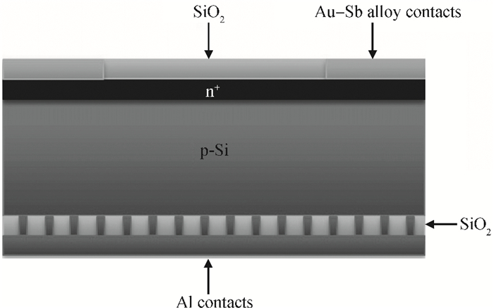
Fig. 1.
Schematic diagram of tellurium supersaturated silicon diode.
SEMICONDUCTOR MATERIALS
Xiyuan Wang, Yongguang Huang, Dewei Liu, Xiaoning Zhu, Xiao Cui and Hongliang Zhu
Corresponding author: Huang Yongguang, Email:yghuang@red.semi.ac.cn
Abstract: Pn junctions based on single crystalline tellurium supersaturated silicon were formed by ion implantation followed by pulsed laser melting (PLM). P type silicon wafers were implanted with 245 keV 126Te+ to a dose of 2×10¹⁵ ions/cm2, after a PLM process (248 nm, laser fluence of 0.30 and 0.35 J/cm2, 1-5 pulses, duration 30 ns), an n+ type single crystalline tellurium supersaturated silicon layer with high carrier density (highest concentration 4.10×1019 cm-3, three orders of magnitude larger than the solid solution limit) was formed, it shows high broadband optical absorption from 400 to 2500 nm. Current-voltage measurements were performed on these diodes under dark and one standard sun (AM 1.5), and good rectification characteristics were observed. For present results, the samples with 4-5 pulses PLM are best.
Key words: tellurium supersaturated silicon pn junction, strong sub-band-gap optical absorption, ion implantation, pulsed laser melting
| [1] |
Wu C, Crouch C H, Zhao L, et al. Near-unity below-band-gap absorption by microstructured silicon. Appl Phys Lett, 2001, 78(13):1850 doi: 10.1063/1.1358846
|
| [2] |
Sheehy M A, Tull B R, Friend C M, et al. Chalcogen doping of silicon via intense femtosecond-laser irradiation. Mater Sci Eng B, 2007, 137:289 doi: 10.1016/j.mseb.2006.10.002
|
| [3] |
Crouch C H, Carey J E, Warrender J M, et al. Comparison of structure and properties of femtosecond and nanosecond laser-structured silicon. Appl Phys Lett, 2004, 84(11):1850 doi: 10.1063/1.1667004
|
| [4] |
Crouch C H, Carey J E, Shen M, et al. Infrared absorption by sulfur-doped silicon formed by femtosecond laser irradiation. Appl Phys A, 2004, 79:1635 doi: 10.1007/s00339-004-2676-0?no-access=true
|
| [5] |
Sheehy M A, Winston L, Carey J E, et al. Role of the background gas in the morphology and optical properties of laser-microstructured silicon. Chem Mater, 2005, 17:3582 doi: 10.1021/cm049029i
|
| [6] |
Tabbal M, Kim T, Woolf D N, et al. Fabrication and sub-band-gap absorption of single-crystal Si supersaturated with Se by pulsed laser mixing. Appl Phys A, 2010, 98:589 doi: 10.1007/s00339-009-5462-1
|
| [7] |
Hu S, Han P, Wang S, et al. Improved photoresponse characteristics in Se-doped Si photodiodes fabricated using picosecond pulsed laser mixing. Semicond Sci Technol, 2012, 27:1 http://www.ingentaconnect.com/content/iop/sst/2012/00000027/00000010/art102002
|
| [8] |
Kim T G, Warrender J M, Aziz M J. Strong sub-band-gap infrared absorption in silicon supersaturated with sulfur. Appl Phys Lett, 2006, 88:241902 doi: 10.1063/1.2212051
|
| [9] |
Bob B P, Kohno A, Charnvanichborikarn S, et al. Fabrication and subband gap optical properties of silicon supersaturated with chalcogens by ion implantation and pulsed laser melting. J Appl Phys, 2010, 107:123506 doi: 10.1063/1.3415544
|
| [10] |
Pan S H, Recht D, Charnvanichborikarn S, et al. Enhanced visible and near-infrared optical absorption in silicon supersaturated with chalcogens. Appl Phys Lett, 2011, 98:121913 doi: 10.1063/1.3567759
|
| [11] |
Carey J E, Crouch C H, Shen M, et al. Visible and near-infrared responsivity of femtosecond-laser microstructured silicon photodiodes. Opt Lett, 2005, 30(14):1773 doi: 10.1364/OL.30.001773
|
| [12] |
Huang Z, Carey J E, Liu M, et al. Microstructured silicon photodetector. Appl Phys Lett, 2006, 89:033506 doi: 10.1063/1.2227629
|
| [13] |
Said A J, Recht D, Sullivan J T, et al. Extended infrared photoresponse and gain in chalcogen-supersaturated silicon photodiodes. Appl Phys Lett, 2011, 99:073503 doi: 10.1063/1.3609871
|
| [14] |
Tull B R, Winkler M T, Mazur E. The role of diffusion in broadband infrared absorption in chalcogen-doped silicon. Appl Phys A, 2009, 96:327 doi: 10.1007/s00339-009-5200-8
|
| [15] |
Shao H, Li Y, Zhang J, et al. Physical mechanisms for the unique optical properties of chalcogen-hyperdoped silicon. Euro Phys Lett, 2012, 99:46005 doi: 10.1209/0295-5075/99/46005
|
| [16] |
Sánchez K, Aguilera I, Palacios P, et al. Formation of a reliable intermediate band in Si heavily coimplanted with chalcogens (S, Se, Te) and group Ⅲ elements (B, Al). Phys Rev B, 2010, 82:165201 doi: 10.1103/PhysRevB.82.165201
|
| [17] |
Wang Xiyuan, Huang Yongguang, Liu Dewei, et al. Fabrication of tellurium doped silicon detector by femtosecond laser and excimer laser. Chinese Journal of Lasers, 2013, 40(3):0302001 doi: 10.3788/CJL
|
| [18] |
Wang Xiyuan, Huang Yongguang, Liu Dewei, et al. High response in a tellurium-supersaturated silicon photodiode. Chin Phys Lett, 2013, 30(3):036101 doi: 10.1088/0256-307X/30/3/036101
|
| [19] |
Her T H, Finlay R J, Wu C, et al. Microstructuring of silicon with femtosecond laser pulses. Appl Phys Lett, 1998, 73(12):1673 doi: 10.1063/1.122241
|
| [20] |
Li Ping, Wang Yu, Feng Guojin, et al. Study of silicon micro-structuring using ultra-short laser pulses. Chinese Journal of Lasers, 2006, 33(12):1688 doi: 10.1007/s00339-004-2676-0?no-access=true
|
| [21] |
Ziegler J F, Ziegler M D, Biersack J P. SRIM-the stopping and range of ions in matter. Nuclear Instruments and Methods in Physics Research B, 2010, 268:1818 doi: 10.1016/j.nimb.2010.02.091
|
| [22] |
Voutsas A T, Hatalis M K, Boyce J, et al. Raman spectroscopy of amorphous and microcrystalline silicon films deposited by low-pressure chemical vapor deposition. J Appl Phys, 1995, 78(12):6999 doi: 10.1063/1.360468
|
| [23] |
Tabbal M, Kim T, Warrender J M, et al. Formation of single crystal sulfur supersaturated silicon based junctions by pulsed laser melting. J Vac Sci Technol B, 2007, 25(6):1847 doi: 10.1116/1.2796184
|
| [24] |
Sheehy M A. Femtosecond-laser microstructuring of silicon:dopants and defects. PhD Dissertation, Harvard University, Cambridge, MA, 2004:27 http://adsabs.harvard.edu/abs/2004PhDT.......230S
|
| [25] |
Narayan J, White C W, Aziz M J, et al. Pulsed excimer (KrF) laser melting of amorphous and crystalline silicon layers. J Appl Phys, 1985, 57(2):564 doi: 10.1063/1.334738
|
| [26] |
Ertekin E, Winkler M T, Recht D, et al. Insulator-to-metal transition in selenium-hyperdoped silicon:observation and origin. Phys Rev Lett, 2012, 108:026401 doi: 10.1103/PhysRevLett.108.026401
|

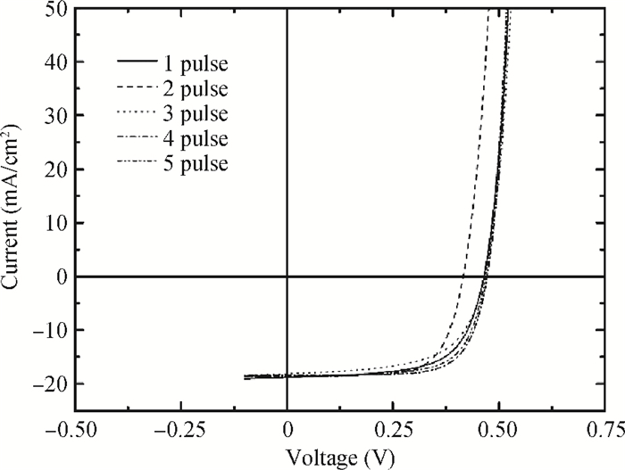
Table 1.
Number of shots, laser fluence, sheet carrier concentration, Hall mobility and carrier to donor ratio for PLM layer of silicon wafer supersaturated with Te at dose of 2

|
| [1] |
Wu C, Crouch C H, Zhao L, et al. Near-unity below-band-gap absorption by microstructured silicon. Appl Phys Lett, 2001, 78(13):1850 doi: 10.1063/1.1358846
|
| [2] |
Sheehy M A, Tull B R, Friend C M, et al. Chalcogen doping of silicon via intense femtosecond-laser irradiation. Mater Sci Eng B, 2007, 137:289 doi: 10.1016/j.mseb.2006.10.002
|
| [3] |
Crouch C H, Carey J E, Warrender J M, et al. Comparison of structure and properties of femtosecond and nanosecond laser-structured silicon. Appl Phys Lett, 2004, 84(11):1850 doi: 10.1063/1.1667004
|
| [4] |
Crouch C H, Carey J E, Shen M, et al. Infrared absorption by sulfur-doped silicon formed by femtosecond laser irradiation. Appl Phys A, 2004, 79:1635 doi: 10.1007/s00339-004-2676-0?no-access=true
|
| [5] |
Sheehy M A, Winston L, Carey J E, et al. Role of the background gas in the morphology and optical properties of laser-microstructured silicon. Chem Mater, 2005, 17:3582 doi: 10.1021/cm049029i
|
| [6] |
Tabbal M, Kim T, Woolf D N, et al. Fabrication and sub-band-gap absorption of single-crystal Si supersaturated with Se by pulsed laser mixing. Appl Phys A, 2010, 98:589 doi: 10.1007/s00339-009-5462-1
|
| [7] |
Hu S, Han P, Wang S, et al. Improved photoresponse characteristics in Se-doped Si photodiodes fabricated using picosecond pulsed laser mixing. Semicond Sci Technol, 2012, 27:1 http://www.ingentaconnect.com/content/iop/sst/2012/00000027/00000010/art102002
|
| [8] |
Kim T G, Warrender J M, Aziz M J. Strong sub-band-gap infrared absorption in silicon supersaturated with sulfur. Appl Phys Lett, 2006, 88:241902 doi: 10.1063/1.2212051
|
| [9] |
Bob B P, Kohno A, Charnvanichborikarn S, et al. Fabrication and subband gap optical properties of silicon supersaturated with chalcogens by ion implantation and pulsed laser melting. J Appl Phys, 2010, 107:123506 doi: 10.1063/1.3415544
|
| [10] |
Pan S H, Recht D, Charnvanichborikarn S, et al. Enhanced visible and near-infrared optical absorption in silicon supersaturated with chalcogens. Appl Phys Lett, 2011, 98:121913 doi: 10.1063/1.3567759
|
| [11] |
Carey J E, Crouch C H, Shen M, et al. Visible and near-infrared responsivity of femtosecond-laser microstructured silicon photodiodes. Opt Lett, 2005, 30(14):1773 doi: 10.1364/OL.30.001773
|
| [12] |
Huang Z, Carey J E, Liu M, et al. Microstructured silicon photodetector. Appl Phys Lett, 2006, 89:033506 doi: 10.1063/1.2227629
|
| [13] |
Said A J, Recht D, Sullivan J T, et al. Extended infrared photoresponse and gain in chalcogen-supersaturated silicon photodiodes. Appl Phys Lett, 2011, 99:073503 doi: 10.1063/1.3609871
|
| [14] |
Tull B R, Winkler M T, Mazur E. The role of diffusion in broadband infrared absorption in chalcogen-doped silicon. Appl Phys A, 2009, 96:327 doi: 10.1007/s00339-009-5200-8
|
| [15] |
Shao H, Li Y, Zhang J, et al. Physical mechanisms for the unique optical properties of chalcogen-hyperdoped silicon. Euro Phys Lett, 2012, 99:46005 doi: 10.1209/0295-5075/99/46005
|
| [16] |
Sánchez K, Aguilera I, Palacios P, et al. Formation of a reliable intermediate band in Si heavily coimplanted with chalcogens (S, Se, Te) and group Ⅲ elements (B, Al). Phys Rev B, 2010, 82:165201 doi: 10.1103/PhysRevB.82.165201
|
| [17] |
Wang Xiyuan, Huang Yongguang, Liu Dewei, et al. Fabrication of tellurium doped silicon detector by femtosecond laser and excimer laser. Chinese Journal of Lasers, 2013, 40(3):0302001 doi: 10.3788/CJL
|
| [18] |
Wang Xiyuan, Huang Yongguang, Liu Dewei, et al. High response in a tellurium-supersaturated silicon photodiode. Chin Phys Lett, 2013, 30(3):036101 doi: 10.1088/0256-307X/30/3/036101
|
| [19] |
Her T H, Finlay R J, Wu C, et al. Microstructuring of silicon with femtosecond laser pulses. Appl Phys Lett, 1998, 73(12):1673 doi: 10.1063/1.122241
|
| [20] |
Li Ping, Wang Yu, Feng Guojin, et al. Study of silicon micro-structuring using ultra-short laser pulses. Chinese Journal of Lasers, 2006, 33(12):1688 doi: 10.1007/s00339-004-2676-0?no-access=true
|
| [21] |
Ziegler J F, Ziegler M D, Biersack J P. SRIM-the stopping and range of ions in matter. Nuclear Instruments and Methods in Physics Research B, 2010, 268:1818 doi: 10.1016/j.nimb.2010.02.091
|
| [22] |
Voutsas A T, Hatalis M K, Boyce J, et al. Raman spectroscopy of amorphous and microcrystalline silicon films deposited by low-pressure chemical vapor deposition. J Appl Phys, 1995, 78(12):6999 doi: 10.1063/1.360468
|
| [23] |
Tabbal M, Kim T, Warrender J M, et al. Formation of single crystal sulfur supersaturated silicon based junctions by pulsed laser melting. J Vac Sci Technol B, 2007, 25(6):1847 doi: 10.1116/1.2796184
|
| [24] |
Sheehy M A. Femtosecond-laser microstructuring of silicon:dopants and defects. PhD Dissertation, Harvard University, Cambridge, MA, 2004:27 http://adsabs.harvard.edu/abs/2004PhDT.......230S
|
| [25] |
Narayan J, White C W, Aziz M J, et al. Pulsed excimer (KrF) laser melting of amorphous and crystalline silicon layers. J Appl Phys, 1985, 57(2):564 doi: 10.1063/1.334738
|
| [26] |
Ertekin E, Winkler M T, Recht D, et al. Insulator-to-metal transition in selenium-hyperdoped silicon:observation and origin. Phys Rev Lett, 2012, 108:026401 doi: 10.1103/PhysRevLett.108.026401
|


Article views: 2206 Times PDF downloads: 9 Times Cited by: 0 Times
Received: 16 November 2012 Revised: 01 December 2012 Online: Published: 01 June 2013
| Citation: |
Xiyuan Wang, Yongguang Huang, Dewei Liu, Xiaoning Zhu, Xiao Cui, Hongliang Zhu. Formation of single crystalline tellurium supersaturated silicon pn junctions by ion implantation followed by pulsed laser melting[J]. Journal of Semiconductors, 2013, 34(6): 063001. doi: 10.1088/1674-4926/34/6/063001
X Y Wang, Y G Huang, D W Liu, X N Zhu, X Cui, H L Zhu. Formation of single crystalline tellurium supersaturated silicon pn junctions by ion implantation followed by pulsed laser melting[J]. J. Semicond., 2013, 34(6): 063001. doi: 10.1088/1674-4926/34/6/063001.
Export: BibTex EndNote

|
| [1] |
Wu C, Crouch C H, Zhao L, et al. Near-unity below-band-gap absorption by microstructured silicon. Appl Phys Lett, 2001, 78(13):1850 doi: 10.1063/1.1358846
|
| [2] |
Sheehy M A, Tull B R, Friend C M, et al. Chalcogen doping of silicon via intense femtosecond-laser irradiation. Mater Sci Eng B, 2007, 137:289 doi: 10.1016/j.mseb.2006.10.002
|
| [3] |
Crouch C H, Carey J E, Warrender J M, et al. Comparison of structure and properties of femtosecond and nanosecond laser-structured silicon. Appl Phys Lett, 2004, 84(11):1850 doi: 10.1063/1.1667004
|
| [4] |
Crouch C H, Carey J E, Shen M, et al. Infrared absorption by sulfur-doped silicon formed by femtosecond laser irradiation. Appl Phys A, 2004, 79:1635 doi: 10.1007/s00339-004-2676-0?no-access=true
|
| [5] |
Sheehy M A, Winston L, Carey J E, et al. Role of the background gas in the morphology and optical properties of laser-microstructured silicon. Chem Mater, 2005, 17:3582 doi: 10.1021/cm049029i
|
| [6] |
Tabbal M, Kim T, Woolf D N, et al. Fabrication and sub-band-gap absorption of single-crystal Si supersaturated with Se by pulsed laser mixing. Appl Phys A, 2010, 98:589 doi: 10.1007/s00339-009-5462-1
|
| [7] |
Hu S, Han P, Wang S, et al. Improved photoresponse characteristics in Se-doped Si photodiodes fabricated using picosecond pulsed laser mixing. Semicond Sci Technol, 2012, 27:1 http://www.ingentaconnect.com/content/iop/sst/2012/00000027/00000010/art102002
|
| [8] |
Kim T G, Warrender J M, Aziz M J. Strong sub-band-gap infrared absorption in silicon supersaturated with sulfur. Appl Phys Lett, 2006, 88:241902 doi: 10.1063/1.2212051
|
| [9] |
Bob B P, Kohno A, Charnvanichborikarn S, et al. Fabrication and subband gap optical properties of silicon supersaturated with chalcogens by ion implantation and pulsed laser melting. J Appl Phys, 2010, 107:123506 doi: 10.1063/1.3415544
|
| [10] |
Pan S H, Recht D, Charnvanichborikarn S, et al. Enhanced visible and near-infrared optical absorption in silicon supersaturated with chalcogens. Appl Phys Lett, 2011, 98:121913 doi: 10.1063/1.3567759
|
| [11] |
Carey J E, Crouch C H, Shen M, et al. Visible and near-infrared responsivity of femtosecond-laser microstructured silicon photodiodes. Opt Lett, 2005, 30(14):1773 doi: 10.1364/OL.30.001773
|
| [12] |
Huang Z, Carey J E, Liu M, et al. Microstructured silicon photodetector. Appl Phys Lett, 2006, 89:033506 doi: 10.1063/1.2227629
|
| [13] |
Said A J, Recht D, Sullivan J T, et al. Extended infrared photoresponse and gain in chalcogen-supersaturated silicon photodiodes. Appl Phys Lett, 2011, 99:073503 doi: 10.1063/1.3609871
|
| [14] |
Tull B R, Winkler M T, Mazur E. The role of diffusion in broadband infrared absorption in chalcogen-doped silicon. Appl Phys A, 2009, 96:327 doi: 10.1007/s00339-009-5200-8
|
| [15] |
Shao H, Li Y, Zhang J, et al. Physical mechanisms for the unique optical properties of chalcogen-hyperdoped silicon. Euro Phys Lett, 2012, 99:46005 doi: 10.1209/0295-5075/99/46005
|
| [16] |
Sánchez K, Aguilera I, Palacios P, et al. Formation of a reliable intermediate band in Si heavily coimplanted with chalcogens (S, Se, Te) and group Ⅲ elements (B, Al). Phys Rev B, 2010, 82:165201 doi: 10.1103/PhysRevB.82.165201
|
| [17] |
Wang Xiyuan, Huang Yongguang, Liu Dewei, et al. Fabrication of tellurium doped silicon detector by femtosecond laser and excimer laser. Chinese Journal of Lasers, 2013, 40(3):0302001 doi: 10.3788/CJL
|
| [18] |
Wang Xiyuan, Huang Yongguang, Liu Dewei, et al. High response in a tellurium-supersaturated silicon photodiode. Chin Phys Lett, 2013, 30(3):036101 doi: 10.1088/0256-307X/30/3/036101
|
| [19] |
Her T H, Finlay R J, Wu C, et al. Microstructuring of silicon with femtosecond laser pulses. Appl Phys Lett, 1998, 73(12):1673 doi: 10.1063/1.122241
|
| [20] |
Li Ping, Wang Yu, Feng Guojin, et al. Study of silicon micro-structuring using ultra-short laser pulses. Chinese Journal of Lasers, 2006, 33(12):1688 doi: 10.1007/s00339-004-2676-0?no-access=true
|
| [21] |
Ziegler J F, Ziegler M D, Biersack J P. SRIM-the stopping and range of ions in matter. Nuclear Instruments and Methods in Physics Research B, 2010, 268:1818 doi: 10.1016/j.nimb.2010.02.091
|
| [22] |
Voutsas A T, Hatalis M K, Boyce J, et al. Raman spectroscopy of amorphous and microcrystalline silicon films deposited by low-pressure chemical vapor deposition. J Appl Phys, 1995, 78(12):6999 doi: 10.1063/1.360468
|
| [23] |
Tabbal M, Kim T, Warrender J M, et al. Formation of single crystal sulfur supersaturated silicon based junctions by pulsed laser melting. J Vac Sci Technol B, 2007, 25(6):1847 doi: 10.1116/1.2796184
|
| [24] |
Sheehy M A. Femtosecond-laser microstructuring of silicon:dopants and defects. PhD Dissertation, Harvard University, Cambridge, MA, 2004:27 http://adsabs.harvard.edu/abs/2004PhDT.......230S
|
| [25] |
Narayan J, White C W, Aziz M J, et al. Pulsed excimer (KrF) laser melting of amorphous and crystalline silicon layers. J Appl Phys, 1985, 57(2):564 doi: 10.1063/1.334738
|
| [26] |
Ertekin E, Winkler M T, Recht D, et al. Insulator-to-metal transition in selenium-hyperdoped silicon:observation and origin. Phys Rev Lett, 2012, 108:026401 doi: 10.1103/PhysRevLett.108.026401
|

 WeChat ID
Journal of Semiconductors © 2017 All Rights Reserved 京ICP备05085259号-2

 DownLoad:

