Fig. 1.
Cross-sectional SEM image of the GOI substrate.
SEMICONDUCTOR MATERIALS
Wang Lin, Yujiao Ruan, Songyan Chen, Cheng Li, Hongkai Lai and Wei Huang
Corresponding author: Chen Songyan, Email:sychen@xmu.edu.cn
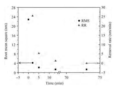
Abstract: We prepared germanium-on-insulator (GOI) substrates by using Smart-CutTM and wafer bonding technology. The fabricated GOI is appropriate for polishing due to a strong bonding strength (2.4 MPa) and a sufficient bonding quality. We investigated mechanical polishing and chemical-mechanical polishing (CMP) systematically, and an appropriate polishing method——mechanical polishing combined with CMP——is obtained. As shown by AFM measurement, the RMS of GOI after polishing decreased to 0.543 nm. And the Ge peak profile of the XRD curve became symmetric, and the FWHM is about 121.7 arcsec, demonstrating a good crystal quality.
Key words: germanium-on-insulator, wafer bonding, mechanical polishing, chemical-mechanical polishing
| [1] |
Bengtsson S. Semiconductor wafer bonding——a review of interfacial properties and applications. J Electron Mater, 1992, 21(8):841
|
| [2] |
Tong Q Y, Scholz R, Gösele U, et al. A "smarter-cut" approach to low temperature silicon layer transfer. Appl Phys Lett, 1998, 72(1):49 doi: 10.1063/1.120601
|
| [3] |
Lasky J B. Wafer bonding for silicon-on-insulator technologies. Appl Phys Lett, 1986, 48(1):78 doi: 10.1063/1.96768
|
| [4] |
Bruel M, Aspar B, Auberton-Hervé A J. Smart-cut:a new silicon on insulator material technology based on hydrogen implantation and wafer bonding. Jpn J Appl Phys, 1997, 36(3):1636 https://ntrs.nasa.gov/archive/nasa/casi.ntrs.nasa.gov/20080009474.pdf
|
| [5] |
Christiansen S H, Singh R, Gösele U. Wafer direct bonding:from advanced substrate engineering to future applications in micro/nanoelectronics. Proc IEEE, 2006, 94(12):2060 doi: 10.1109/JPROC.2006.886026
|
| [6] |
Zhu Z H, Ejeckam F E, Qian Y, et al. Wafer bonding technology and its applications in optoelectronic devices and materials. IEEE J Sel Top Quantum Electron, 1997, 3(3):927 doi: 10.1109/2944.640646
|
| [7] |
Tong Q Y, Huang L J, Gösele U M. Transfer of semiconductor and oxide films by wafer bonding and layer cutting. J Electron Mater, 2000, 29(7):928 doi: 10.1007/s11664-000-0183-4
|
| [8] |
Kittler M, Reiche M, Arguirov T, et al. Silicon-based light emitters. Phys Status Solidi A, 2006, 203(4):802 doi: 10.1002/pssa.v203:4
|
| [9] |
Gundel P, Schubert M C, Kwapil W, et al. Micro-photoluminescence spectroscopy on metal precipitates insilicon. Phys Status Solidi (RRL), 2009, 3(7):230 http://publica.fraunhofer.de/documents/N-113410.html
|
| [10] |
Nakaharai S, Tezuka T, Hirashita N, et al. Formation process of high-purity Ge-on-insulator layers by Ge-condensation technique. J Appl Phys, 2009, 105(2):024515 doi: 10.1063/1.3068339
|
| [11] |
Liu Y, Deal M D, Plummer J D. High-quality single-crystal Ge on insulator by liquid-phase epitaxy on Si substrates. Appl Phys Lett, 2004, 84(14):2563 doi: 10.1063/1.1691175
|
| [12] |
Akatsu T, Deguet C, Sanchez L, et al. Germanium-on-insulator (GeOI) substrates——a novel engineered substrate for future high performance devices. Mater Sci Semicond Process, 2006, 9(4):444
|
| [13] |
Jin H Y, Liu E Z, Cheung N W. Fabrication and characteristics of germanium-on-insulator substrates. 9th International Conference on Solid-State and Integrated-Circuit Technology, ICSICT, 2008:662
|
| [14] |
Tracy C J, Fejes P, Theodore N D, et al. Germanium-on-insulator substrates by wafer bonding. J Electron Mater, 2004, 33(8):886 doi: 10.1007/s11664-004-0216-5
|
| [15] |
Deguet C, Dechamp J, Morales C, et al. 200 mm germanium-on-insulator (GeOI) structures realized from epitaxial wafers using the Smart CutTM technology. The Electrochemical Society Proceedings, 2005, 2:78 http://proceedings.spiedigitallibrary.org/proceeding.aspx?articleid=2605861
|
| [16] |
Chao Y L, Scholz R, Reiche M, et al. Characteristics of germanium-on-insulators fabricated by wafer bonding and hydrogen-induced layer splitting. Jpn J Appl Phys, 2005, 45(11):8565 http://www.seas.ucla.edu/cmoslab/resumes/yu-lin_CV.pdf
|
| [17] |
Taraschi G, Pitera A J, Fitzgerald E A. Strained Si, SiGe, and Ge on-insulator:review of wafer bonding fabrication techniques. Solid-State Electron, 2004, 48(8):1297 doi: 10.1016/j.sse.2004.01.012
|
| [18] |
Akatsu T, Deguet C, Sanchez L, et al. 200 mm germanium-on-insulator (GeOI) by Smart CutTM technology and recent GeOI pMOSFETs achievements 200 mm germanium-on-insulator (GeOI) by Smart CutTM technology and recent GeOI pMOSFETs achievements. IEEE International SOI Conference, 2005:137
|
| [19] |
Deguet C, Sanchez L, Akatsu T, et al. Fabrication and characterisation of 200 mm germanium-on-insulator (GeOI) substrates made from bulk germanium. Electron Lett, 2006, 42(7):415 doi: 10.1049/el:20060208
|
| [20] |
Dissanayake S, Tomiyama K, Sugahara S, et al. High performance ultrathin (110)-oriented Ge-on-insulator p-channel metal-oxide-semiconductor field-effect transistors fabricated by Ge condensation technique. Appl Phys Express, 2010, 3(4):041302 doi: 10.1143/APEX.3.041302
|
| [21] |
Chen L, Dong P, Lipson M. High performance germanium photodetectors integrated on submicron silicon waveguides by low temperature wafer bonding. Opt Express, 2008, 16(15):11513 doi: 10.1364/OE.16.011513
|
| [22] |
Peddeti S, Ong P, Leunissen L H A, et al. Chemical mechanical polishing of Ge using colloidal silica particles and H2O2. Electrochem Solid-State Lett, 2011, 14(7):H254 doi: 10.1149/1.3575166
|
| [23] |
Zhao Q. Research of CMP and clean technology on Ge polished wafer. Master Thesis, Tianjin University, 2008
|
| [24] |
Ruan Y, Liu R, Lin W, et al. Impacts of thermal annealing on hydrogen-implanted germanium and germanium-on-insulator substrates. JES, 2011, 158(11):A1
|
| [25] |
Hydrick J M, Park J S, Bai J, et al. Chemical mechanical polishing of epitaxial germanium on SiO2-patterned Si(001) substrates. ECS Trans, 2008, 16(10):237 http://ecst.ecsdl.org/content/16/10/237.short
|
| [26] |
Yin Kangda, Wang Shengli, Liu Yuling, et al. Evaluation of planarization capability of copper slurry in the CMP process. Journal of Semiconductors, 2013, 34(3):036002 doi: 10.1088/1674-4926/34/3/036002
|
| [27] |
Li Y, Hariharaputhiran M, Babu S V. Chemical-mechanical polishing of copper and tantalum with silica abrasives. J Mater Res, 2001, 16(4):1066 doi: 10.1557/JMR.2001.0148
|
| [28] |
Krishnan M, Nalaskowski J W, Cook L M. Chemical mechanical planarization:slurry chemistry, materials, and mechanisms. Chem Rev, 2010, 110(1):178 doi: 10.1021/cr900170z
|
| [29] |
Sze S M. Physics of semiconductor devices. New York:John Wiley & Sons, 1981
|
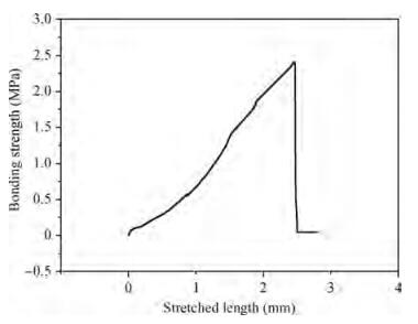
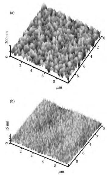
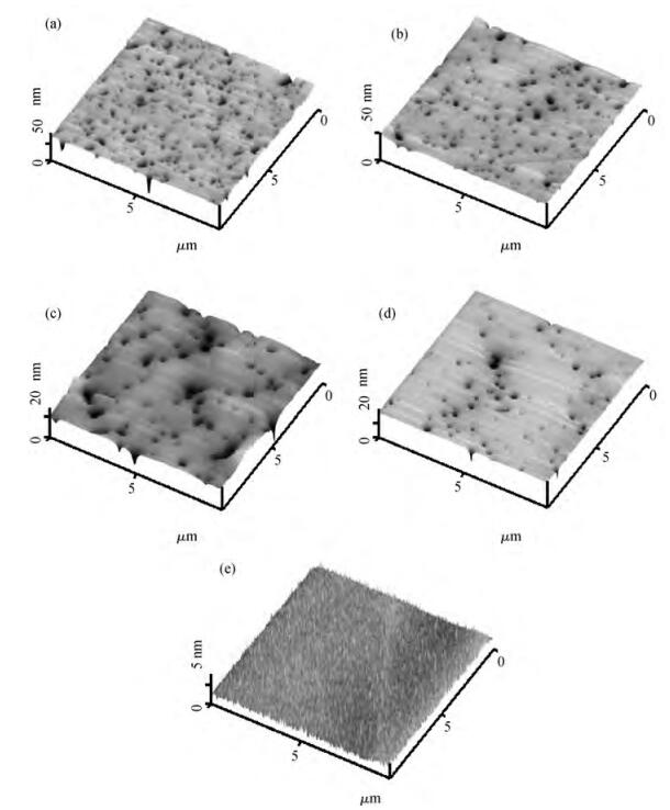
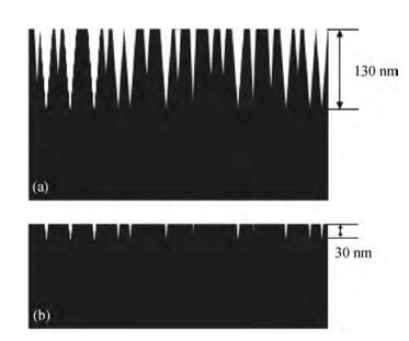
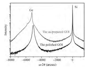
Table 1. Polishing conditions used for samples A and B. Pressure: 1 kg; Rotational speed of the polishing pad and chuck: 33 rpm and 30 rpm.

|
| [1] |
Bengtsson S. Semiconductor wafer bonding——a review of interfacial properties and applications. J Electron Mater, 1992, 21(8):841
|
| [2] |
Tong Q Y, Scholz R, Gösele U, et al. A "smarter-cut" approach to low temperature silicon layer transfer. Appl Phys Lett, 1998, 72(1):49 doi: 10.1063/1.120601
|
| [3] |
Lasky J B. Wafer bonding for silicon-on-insulator technologies. Appl Phys Lett, 1986, 48(1):78 doi: 10.1063/1.96768
|
| [4] |
Bruel M, Aspar B, Auberton-Hervé A J. Smart-cut:a new silicon on insulator material technology based on hydrogen implantation and wafer bonding. Jpn J Appl Phys, 1997, 36(3):1636 https://ntrs.nasa.gov/archive/nasa/casi.ntrs.nasa.gov/20080009474.pdf
|
| [5] |
Christiansen S H, Singh R, Gösele U. Wafer direct bonding:from advanced substrate engineering to future applications in micro/nanoelectronics. Proc IEEE, 2006, 94(12):2060 doi: 10.1109/JPROC.2006.886026
|
| [6] |
Zhu Z H, Ejeckam F E, Qian Y, et al. Wafer bonding technology and its applications in optoelectronic devices and materials. IEEE J Sel Top Quantum Electron, 1997, 3(3):927 doi: 10.1109/2944.640646
|
| [7] |
Tong Q Y, Huang L J, Gösele U M. Transfer of semiconductor and oxide films by wafer bonding and layer cutting. J Electron Mater, 2000, 29(7):928 doi: 10.1007/s11664-000-0183-4
|
| [8] |
Kittler M, Reiche M, Arguirov T, et al. Silicon-based light emitters. Phys Status Solidi A, 2006, 203(4):802 doi: 10.1002/pssa.v203:4
|
| [9] |
Gundel P, Schubert M C, Kwapil W, et al. Micro-photoluminescence spectroscopy on metal precipitates insilicon. Phys Status Solidi (RRL), 2009, 3(7):230 http://publica.fraunhofer.de/documents/N-113410.html
|
| [10] |
Nakaharai S, Tezuka T, Hirashita N, et al. Formation process of high-purity Ge-on-insulator layers by Ge-condensation technique. J Appl Phys, 2009, 105(2):024515 doi: 10.1063/1.3068339
|
| [11] |
Liu Y, Deal M D, Plummer J D. High-quality single-crystal Ge on insulator by liquid-phase epitaxy on Si substrates. Appl Phys Lett, 2004, 84(14):2563 doi: 10.1063/1.1691175
|
| [12] |
Akatsu T, Deguet C, Sanchez L, et al. Germanium-on-insulator (GeOI) substrates——a novel engineered substrate for future high performance devices. Mater Sci Semicond Process, 2006, 9(4):444
|
| [13] |
Jin H Y, Liu E Z, Cheung N W. Fabrication and characteristics of germanium-on-insulator substrates. 9th International Conference on Solid-State and Integrated-Circuit Technology, ICSICT, 2008:662
|
| [14] |
Tracy C J, Fejes P, Theodore N D, et al. Germanium-on-insulator substrates by wafer bonding. J Electron Mater, 2004, 33(8):886 doi: 10.1007/s11664-004-0216-5
|
| [15] |
Deguet C, Dechamp J, Morales C, et al. 200 mm germanium-on-insulator (GeOI) structures realized from epitaxial wafers using the Smart CutTM technology. The Electrochemical Society Proceedings, 2005, 2:78 http://proceedings.spiedigitallibrary.org/proceeding.aspx?articleid=2605861
|
| [16] |
Chao Y L, Scholz R, Reiche M, et al. Characteristics of germanium-on-insulators fabricated by wafer bonding and hydrogen-induced layer splitting. Jpn J Appl Phys, 2005, 45(11):8565 http://www.seas.ucla.edu/cmoslab/resumes/yu-lin_CV.pdf
|
| [17] |
Taraschi G, Pitera A J, Fitzgerald E A. Strained Si, SiGe, and Ge on-insulator:review of wafer bonding fabrication techniques. Solid-State Electron, 2004, 48(8):1297 doi: 10.1016/j.sse.2004.01.012
|
| [18] |
Akatsu T, Deguet C, Sanchez L, et al. 200 mm germanium-on-insulator (GeOI) by Smart CutTM technology and recent GeOI pMOSFETs achievements 200 mm germanium-on-insulator (GeOI) by Smart CutTM technology and recent GeOI pMOSFETs achievements. IEEE International SOI Conference, 2005:137
|
| [19] |
Deguet C, Sanchez L, Akatsu T, et al. Fabrication and characterisation of 200 mm germanium-on-insulator (GeOI) substrates made from bulk germanium. Electron Lett, 2006, 42(7):415 doi: 10.1049/el:20060208
|
| [20] |
Dissanayake S, Tomiyama K, Sugahara S, et al. High performance ultrathin (110)-oriented Ge-on-insulator p-channel metal-oxide-semiconductor field-effect transistors fabricated by Ge condensation technique. Appl Phys Express, 2010, 3(4):041302 doi: 10.1143/APEX.3.041302
|
| [21] |
Chen L, Dong P, Lipson M. High performance germanium photodetectors integrated on submicron silicon waveguides by low temperature wafer bonding. Opt Express, 2008, 16(15):11513 doi: 10.1364/OE.16.011513
|
| [22] |
Peddeti S, Ong P, Leunissen L H A, et al. Chemical mechanical polishing of Ge using colloidal silica particles and H2O2. Electrochem Solid-State Lett, 2011, 14(7):H254 doi: 10.1149/1.3575166
|
| [23] |
Zhao Q. Research of CMP and clean technology on Ge polished wafer. Master Thesis, Tianjin University, 2008
|
| [24] |
Ruan Y, Liu R, Lin W, et al. Impacts of thermal annealing on hydrogen-implanted germanium and germanium-on-insulator substrates. JES, 2011, 158(11):A1
|
| [25] |
Hydrick J M, Park J S, Bai J, et al. Chemical mechanical polishing of epitaxial germanium on SiO2-patterned Si(001) substrates. ECS Trans, 2008, 16(10):237 http://ecst.ecsdl.org/content/16/10/237.short
|
| [26] |
Yin Kangda, Wang Shengli, Liu Yuling, et al. Evaluation of planarization capability of copper slurry in the CMP process. Journal of Semiconductors, 2013, 34(3):036002 doi: 10.1088/1674-4926/34/3/036002
|
| [27] |
Li Y, Hariharaputhiran M, Babu S V. Chemical-mechanical polishing of copper and tantalum with silica abrasives. J Mater Res, 2001, 16(4):1066 doi: 10.1557/JMR.2001.0148
|
| [28] |
Krishnan M, Nalaskowski J W, Cook L M. Chemical mechanical planarization:slurry chemistry, materials, and mechanisms. Chem Rev, 2010, 110(1):178 doi: 10.1021/cr900170z
|
| [29] |
Sze S M. Physics of semiconductor devices. New York:John Wiley & Sons, 1981
|


Article views: 2442 Times PDF downloads: 18 Times Cited by: 0 Times
Received: 28 March 2013 Revised: 06 May 2013 Online: Published: 01 August 2013
| Citation: |
Wang Lin, Yujiao Ruan, Songyan Chen, Cheng Li, Hongkai Lai, Wei Huang. The impact of polishing on germanium-on-insulator substrates[J]. Journal of Semiconductors, 2013, 34(8): 083005. doi: 10.1088/1674-4926/34/8/083005
W Lin, Y J Ruan, S Y Chen, C Li, H K Lai, W Huang. The impact of polishing on germanium-on-insulator substrates[J]. J. Semicond., 2013, 34(8): 083005. doi: 10.1088/1674-4926/34/8/083005.
Export: BibTex EndNote

|
| [1] |
Bengtsson S. Semiconductor wafer bonding——a review of interfacial properties and applications. J Electron Mater, 1992, 21(8):841
|
| [2] |
Tong Q Y, Scholz R, Gösele U, et al. A "smarter-cut" approach to low temperature silicon layer transfer. Appl Phys Lett, 1998, 72(1):49 doi: 10.1063/1.120601
|
| [3] |
Lasky J B. Wafer bonding for silicon-on-insulator technologies. Appl Phys Lett, 1986, 48(1):78 doi: 10.1063/1.96768
|
| [4] |
Bruel M, Aspar B, Auberton-Hervé A J. Smart-cut:a new silicon on insulator material technology based on hydrogen implantation and wafer bonding. Jpn J Appl Phys, 1997, 36(3):1636 https://ntrs.nasa.gov/archive/nasa/casi.ntrs.nasa.gov/20080009474.pdf
|
| [5] |
Christiansen S H, Singh R, Gösele U. Wafer direct bonding:from advanced substrate engineering to future applications in micro/nanoelectronics. Proc IEEE, 2006, 94(12):2060 doi: 10.1109/JPROC.2006.886026
|
| [6] |
Zhu Z H, Ejeckam F E, Qian Y, et al. Wafer bonding technology and its applications in optoelectronic devices and materials. IEEE J Sel Top Quantum Electron, 1997, 3(3):927 doi: 10.1109/2944.640646
|
| [7] |
Tong Q Y, Huang L J, Gösele U M. Transfer of semiconductor and oxide films by wafer bonding and layer cutting. J Electron Mater, 2000, 29(7):928 doi: 10.1007/s11664-000-0183-4
|
| [8] |
Kittler M, Reiche M, Arguirov T, et al. Silicon-based light emitters. Phys Status Solidi A, 2006, 203(4):802 doi: 10.1002/pssa.v203:4
|
| [9] |
Gundel P, Schubert M C, Kwapil W, et al. Micro-photoluminescence spectroscopy on metal precipitates insilicon. Phys Status Solidi (RRL), 2009, 3(7):230 http://publica.fraunhofer.de/documents/N-113410.html
|
| [10] |
Nakaharai S, Tezuka T, Hirashita N, et al. Formation process of high-purity Ge-on-insulator layers by Ge-condensation technique. J Appl Phys, 2009, 105(2):024515 doi: 10.1063/1.3068339
|
| [11] |
Liu Y, Deal M D, Plummer J D. High-quality single-crystal Ge on insulator by liquid-phase epitaxy on Si substrates. Appl Phys Lett, 2004, 84(14):2563 doi: 10.1063/1.1691175
|
| [12] |
Akatsu T, Deguet C, Sanchez L, et al. Germanium-on-insulator (GeOI) substrates——a novel engineered substrate for future high performance devices. Mater Sci Semicond Process, 2006, 9(4):444
|
| [13] |
Jin H Y, Liu E Z, Cheung N W. Fabrication and characteristics of germanium-on-insulator substrates. 9th International Conference on Solid-State and Integrated-Circuit Technology, ICSICT, 2008:662
|
| [14] |
Tracy C J, Fejes P, Theodore N D, et al. Germanium-on-insulator substrates by wafer bonding. J Electron Mater, 2004, 33(8):886 doi: 10.1007/s11664-004-0216-5
|
| [15] |
Deguet C, Dechamp J, Morales C, et al. 200 mm germanium-on-insulator (GeOI) structures realized from epitaxial wafers using the Smart CutTM technology. The Electrochemical Society Proceedings, 2005, 2:78 http://proceedings.spiedigitallibrary.org/proceeding.aspx?articleid=2605861
|
| [16] |
Chao Y L, Scholz R, Reiche M, et al. Characteristics of germanium-on-insulators fabricated by wafer bonding and hydrogen-induced layer splitting. Jpn J Appl Phys, 2005, 45(11):8565 http://www.seas.ucla.edu/cmoslab/resumes/yu-lin_CV.pdf
|
| [17] |
Taraschi G, Pitera A J, Fitzgerald E A. Strained Si, SiGe, and Ge on-insulator:review of wafer bonding fabrication techniques. Solid-State Electron, 2004, 48(8):1297 doi: 10.1016/j.sse.2004.01.012
|
| [18] |
Akatsu T, Deguet C, Sanchez L, et al. 200 mm germanium-on-insulator (GeOI) by Smart CutTM technology and recent GeOI pMOSFETs achievements 200 mm germanium-on-insulator (GeOI) by Smart CutTM technology and recent GeOI pMOSFETs achievements. IEEE International SOI Conference, 2005:137
|
| [19] |
Deguet C, Sanchez L, Akatsu T, et al. Fabrication and characterisation of 200 mm germanium-on-insulator (GeOI) substrates made from bulk germanium. Electron Lett, 2006, 42(7):415 doi: 10.1049/el:20060208
|
| [20] |
Dissanayake S, Tomiyama K, Sugahara S, et al. High performance ultrathin (110)-oriented Ge-on-insulator p-channel metal-oxide-semiconductor field-effect transistors fabricated by Ge condensation technique. Appl Phys Express, 2010, 3(4):041302 doi: 10.1143/APEX.3.041302
|
| [21] |
Chen L, Dong P, Lipson M. High performance germanium photodetectors integrated on submicron silicon waveguides by low temperature wafer bonding. Opt Express, 2008, 16(15):11513 doi: 10.1364/OE.16.011513
|
| [22] |
Peddeti S, Ong P, Leunissen L H A, et al. Chemical mechanical polishing of Ge using colloidal silica particles and H2O2. Electrochem Solid-State Lett, 2011, 14(7):H254 doi: 10.1149/1.3575166
|
| [23] |
Zhao Q. Research of CMP and clean technology on Ge polished wafer. Master Thesis, Tianjin University, 2008
|
| [24] |
Ruan Y, Liu R, Lin W, et al. Impacts of thermal annealing on hydrogen-implanted germanium and germanium-on-insulator substrates. JES, 2011, 158(11):A1
|
| [25] |
Hydrick J M, Park J S, Bai J, et al. Chemical mechanical polishing of epitaxial germanium on SiO2-patterned Si(001) substrates. ECS Trans, 2008, 16(10):237 http://ecst.ecsdl.org/content/16/10/237.short
|
| [26] |
Yin Kangda, Wang Shengli, Liu Yuling, et al. Evaluation of planarization capability of copper slurry in the CMP process. Journal of Semiconductors, 2013, 34(3):036002 doi: 10.1088/1674-4926/34/3/036002
|
| [27] |
Li Y, Hariharaputhiran M, Babu S V. Chemical-mechanical polishing of copper and tantalum with silica abrasives. J Mater Res, 2001, 16(4):1066 doi: 10.1557/JMR.2001.0148
|
| [28] |
Krishnan M, Nalaskowski J W, Cook L M. Chemical mechanical planarization:slurry chemistry, materials, and mechanisms. Chem Rev, 2010, 110(1):178 doi: 10.1021/cr900170z
|
| [29] |
Sze S M. Physics of semiconductor devices. New York:John Wiley & Sons, 1981
|

 WeChat ID
Journal of Semiconductors © 2017 All Rights Reserved 京ICP备05085259号-2

 DownLoad: