


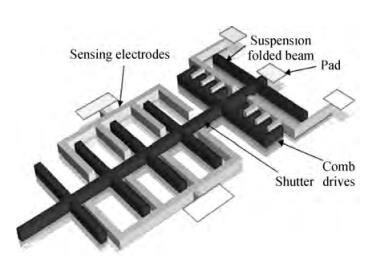
Fig. 1.
Novel SOI-based miniature electric field sensor structure diagram.
SEMICONDUCTOR TECHNOLOGY
Wei Liu1, 2, , Pengfei Yang1, 2, Chunrong Peng1, Dongming Fang1 and Shanhong Xia1
Corresponding author: Liu Wei, Email:lwgreat_2006@yahoo.com.cn; Xia Shanhong, shxia@mail.ie.ac.cn
Abstract: This paper presents a new fabrication process for the SOI-based novel miniature electric field sensor. This new process uses polyimide film to release the SiO2 layer. Compared with the CO2 critical point release method, it significantly improves the device surface cleanliness and shortens the process flow. The impurity on the base layer is analyzed. The problem of peak and butterfly-type contamination occurring on the base layer of the SOI wafer during the DRIE process is discussed and solved by thickening the photoresist layer and coating with polyimide film twice. This new process could fabricate MEMS sensors and actuators such as SOI-based electric field sensors, gyroscopes, and micro mirrors and can be an alternative fabrication process compared to commercial SOIMUMPS fabrication processes.
Key words: electrostatic field sensor, SOI, sacrificial layer release, polyimide, DRIE
| [1] |
Peng Chunrong, Chen Xianxiang, Xia Shanhong. Electric field micro-sensor based on electrostatic comb-driven and differential detecting. Chinese Mechanical Engine, 2005, 16:171
|
| [2] |
Riehl P, Scott K, Muller R, et al, Electrostatic charge and field sensors based on micromechanical resonators. J Microelectromech Syst, 2003, 12(5):577 doi: 10.1109/JMEMS.2003.818066
|
| [3] |
Ye Chao, Chen Xianxiang, Peng Chunrong. Application of two thermal actuators in miniature electric field sensors. Chinese Journal of Semiconductors, 2006, 27(9):1572
|
| [4] |
Guo Xin, Peng Chunrong, Xia Shanhong. Some methods for preventing release stiction of MEFS. Instrument Technique and Sensor, 2009, supple:328
|
| [5] |
Yang Pengfei, Peng Chunrong, Xia Shanhong. Design and testing of a SOI electric-field microsensor. Journal of Electronics & Information Technology, 2011, 33(11):2771
|
| [6] |
Lee H S, Yoon J B. A simple and effective lift-off with positive Photoresist. J Micromechan Microeng, 2005, 15:2136 doi: 10.1088/0960-1317/15/11/020
|
| [7] |
Raccurt O, Tardif F, Arnaud d'Avitaya F, et al. Influence of liquid surface tension on stiction of SOI MEMS. J Micromechan Microeng, 2004, 14:1083 doi: 10.1088/0960-1317/14/7/031
|
| [8] |
Hui Yu, Jing Yupeng. Supercritical carbon dioxide process for releasing stuck cantilever beams. Journal of Semiconductors, 2010, 31(10):106001 doi: 10.1088/1674-4926/31/10/106001
|
| [9] |
Ashursta W R, Carraroa C, Maboudiana R, et al. Wafer level anti-stiction coatings for MEMS. Sensors and Actuators A, 2003, 104:213 doi: 10.1016/S0924-4247(03)00023-2
|
| [10] |
Xiao S Y, Che L F, Wang Y L. A novel fabrication process of MEMS devices on polyimide flexible substrates. Microelectron Eng, 2008, 85:452 doi: 10.1016/j.mee.2007.08.004
|
| [11] |
Alper S E, Azgin K, Akin T. A high-performance silicon-on-insulator MEMS gyroscope operating at atmospheric pressure. Sensors and Actuators A, 2007, 135:34 doi: 10.1016/j.sna.2006.06.043
|
| [12] |
Singh J, Teo J H S, Xu Y, et al. A two axes scanning SOI MEMS micromirror for endoscopic bioimaging. J Micromechan Microeng, 2008, 18:025001 doi: 10.1088/0960-1317/18/2/025001
|
| [13] |
Mukhopadhyay D, Dong J, Pengwang E. A SOI-MEMS-based 3-DOF planar parallel-kinematics nanopositioning stage. Sensors and Actuators A:Physical, 2008, 147:340 doi: 10.1016/j.sna.2008.04.018
|
| [14] |
Lin C W, Yang H A, Wang W C. Implementation of three-dimensional SOI-MEMS wafer-level packaging using through-wafer interconnections. J Micromechan Microeng, 2007, 17:1200 doi: 10.1088/0960-1317/17/6/014
|
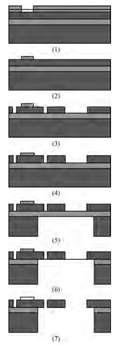

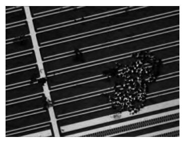
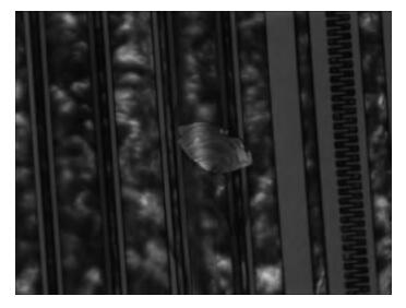
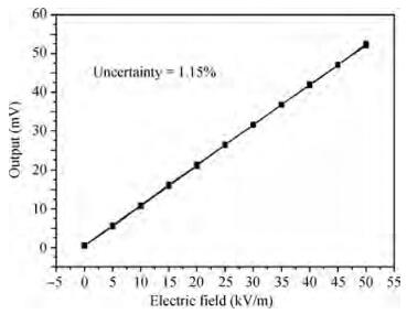
Table 1.
Preparation steps for the CO

|
Table 2. Percentage of elements contained in the impurity.

|
| [1] |
Peng Chunrong, Chen Xianxiang, Xia Shanhong. Electric field micro-sensor based on electrostatic comb-driven and differential detecting. Chinese Mechanical Engine, 2005, 16:171
|
| [2] |
Riehl P, Scott K, Muller R, et al, Electrostatic charge and field sensors based on micromechanical resonators. J Microelectromech Syst, 2003, 12(5):577 doi: 10.1109/JMEMS.2003.818066
|
| [3] |
Ye Chao, Chen Xianxiang, Peng Chunrong. Application of two thermal actuators in miniature electric field sensors. Chinese Journal of Semiconductors, 2006, 27(9):1572
|
| [4] |
Guo Xin, Peng Chunrong, Xia Shanhong. Some methods for preventing release stiction of MEFS. Instrument Technique and Sensor, 2009, supple:328
|
| [5] |
Yang Pengfei, Peng Chunrong, Xia Shanhong. Design and testing of a SOI electric-field microsensor. Journal of Electronics & Information Technology, 2011, 33(11):2771
|
| [6] |
Lee H S, Yoon J B. A simple and effective lift-off with positive Photoresist. J Micromechan Microeng, 2005, 15:2136 doi: 10.1088/0960-1317/15/11/020
|
| [7] |
Raccurt O, Tardif F, Arnaud d'Avitaya F, et al. Influence of liquid surface tension on stiction of SOI MEMS. J Micromechan Microeng, 2004, 14:1083 doi: 10.1088/0960-1317/14/7/031
|
| [8] |
Hui Yu, Jing Yupeng. Supercritical carbon dioxide process for releasing stuck cantilever beams. Journal of Semiconductors, 2010, 31(10):106001 doi: 10.1088/1674-4926/31/10/106001
|
| [9] |
Ashursta W R, Carraroa C, Maboudiana R, et al. Wafer level anti-stiction coatings for MEMS. Sensors and Actuators A, 2003, 104:213 doi: 10.1016/S0924-4247(03)00023-2
|
| [10] |
Xiao S Y, Che L F, Wang Y L. A novel fabrication process of MEMS devices on polyimide flexible substrates. Microelectron Eng, 2008, 85:452 doi: 10.1016/j.mee.2007.08.004
|
| [11] |
Alper S E, Azgin K, Akin T. A high-performance silicon-on-insulator MEMS gyroscope operating at atmospheric pressure. Sensors and Actuators A, 2007, 135:34 doi: 10.1016/j.sna.2006.06.043
|
| [12] |
Singh J, Teo J H S, Xu Y, et al. A two axes scanning SOI MEMS micromirror for endoscopic bioimaging. J Micromechan Microeng, 2008, 18:025001 doi: 10.1088/0960-1317/18/2/025001
|
| [13] |
Mukhopadhyay D, Dong J, Pengwang E. A SOI-MEMS-based 3-DOF planar parallel-kinematics nanopositioning stage. Sensors and Actuators A:Physical, 2008, 147:340 doi: 10.1016/j.sna.2008.04.018
|
| [14] |
Lin C W, Yang H A, Wang W C. Implementation of three-dimensional SOI-MEMS wafer-level packaging using through-wafer interconnections. J Micromechan Microeng, 2007, 17:1200 doi: 10.1088/0960-1317/17/6/014
|


Article views: 2107 Times PDF downloads: 14 Times Cited by: 0 Times
Received: 17 January 2013 Revised: 29 March 2013 Online: Published: 01 August 2013
| Citation: |
Wei Liu, Pengfei Yang, Chunrong Peng, Dongming Fang, Shanhong Xia. A new fabrication process for the SOI-based miniature electric field sensor[J]. Journal of Semiconductors, 2013, 34(8): 086005. doi: 10.1088/1674-4926/34/8/086005
W Liu, P F Yang, C R Peng, D M Fang, S H Xia. A new fabrication process for the SOI-based miniature electric field sensor[J]. J. Semicond., 2013, 34(8): 086005. doi: 10.1088/1674-4926/34/8/086005.
Export: BibTex EndNote

|
| [1] |
Peng Chunrong, Chen Xianxiang, Xia Shanhong. Electric field micro-sensor based on electrostatic comb-driven and differential detecting. Chinese Mechanical Engine, 2005, 16:171
|
| [2] |
Riehl P, Scott K, Muller R, et al, Electrostatic charge and field sensors based on micromechanical resonators. J Microelectromech Syst, 2003, 12(5):577 doi: 10.1109/JMEMS.2003.818066
|
| [3] |
Ye Chao, Chen Xianxiang, Peng Chunrong. Application of two thermal actuators in miniature electric field sensors. Chinese Journal of Semiconductors, 2006, 27(9):1572
|
| [4] |
Guo Xin, Peng Chunrong, Xia Shanhong. Some methods for preventing release stiction of MEFS. Instrument Technique and Sensor, 2009, supple:328
|
| [5] |
Yang Pengfei, Peng Chunrong, Xia Shanhong. Design and testing of a SOI electric-field microsensor. Journal of Electronics & Information Technology, 2011, 33(11):2771
|
| [6] |
Lee H S, Yoon J B. A simple and effective lift-off with positive Photoresist. J Micromechan Microeng, 2005, 15:2136 doi: 10.1088/0960-1317/15/11/020
|
| [7] |
Raccurt O, Tardif F, Arnaud d'Avitaya F, et al. Influence of liquid surface tension on stiction of SOI MEMS. J Micromechan Microeng, 2004, 14:1083 doi: 10.1088/0960-1317/14/7/031
|
| [8] |
Hui Yu, Jing Yupeng. Supercritical carbon dioxide process for releasing stuck cantilever beams. Journal of Semiconductors, 2010, 31(10):106001 doi: 10.1088/1674-4926/31/10/106001
|
| [9] |
Ashursta W R, Carraroa C, Maboudiana R, et al. Wafer level anti-stiction coatings for MEMS. Sensors and Actuators A, 2003, 104:213 doi: 10.1016/S0924-4247(03)00023-2
|
| [10] |
Xiao S Y, Che L F, Wang Y L. A novel fabrication process of MEMS devices on polyimide flexible substrates. Microelectron Eng, 2008, 85:452 doi: 10.1016/j.mee.2007.08.004
|
| [11] |
Alper S E, Azgin K, Akin T. A high-performance silicon-on-insulator MEMS gyroscope operating at atmospheric pressure. Sensors and Actuators A, 2007, 135:34 doi: 10.1016/j.sna.2006.06.043
|
| [12] |
Singh J, Teo J H S, Xu Y, et al. A two axes scanning SOI MEMS micromirror for endoscopic bioimaging. J Micromechan Microeng, 2008, 18:025001 doi: 10.1088/0960-1317/18/2/025001
|
| [13] |
Mukhopadhyay D, Dong J, Pengwang E. A SOI-MEMS-based 3-DOF planar parallel-kinematics nanopositioning stage. Sensors and Actuators A:Physical, 2008, 147:340 doi: 10.1016/j.sna.2008.04.018
|
| [14] |
Lin C W, Yang H A, Wang W C. Implementation of three-dimensional SOI-MEMS wafer-level packaging using through-wafer interconnections. J Micromechan Microeng, 2007, 17:1200 doi: 10.1088/0960-1317/17/6/014
|

 WeChat ID
Journal of Semiconductors © 2017 All Rights Reserved 京ICP备05085259号-2

 DownLoad:

