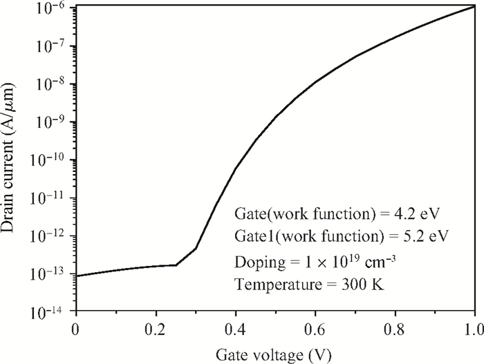
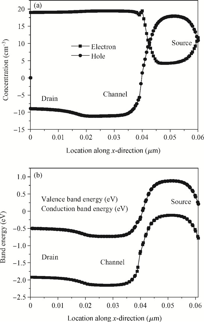
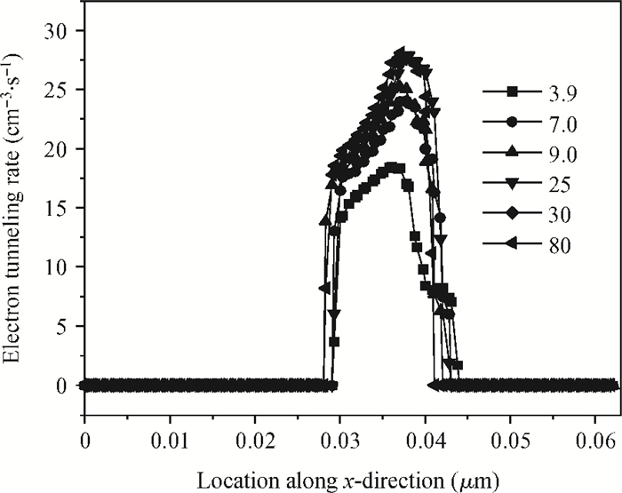
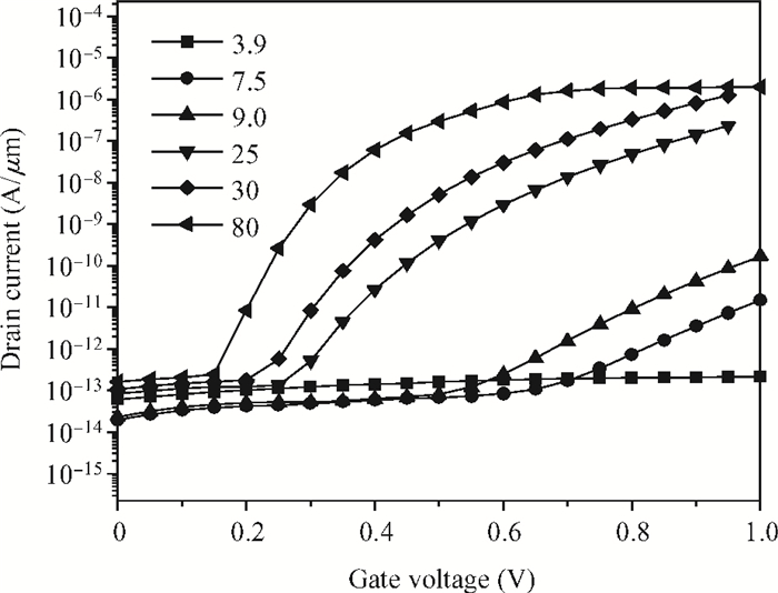
SEMICONDUCTOR DEVICES

A simulation-based proposed high-k heterostructure AlGaAs/Si junctionless n-type tunnel FET

Shiromani Balmukund Rahi1, Bahniman Ghosh2, and Pranav Asthana1

+ Author Affiliations

 Corresponding author: Bahniman Ghosh, Email:bghosh@utexas.edu

PDF

Abstract: We propose a heterostructure junctionless tunnel field effect transistor (HJL-TFET) using AlGaAs/Si. In the proposed HJL-TFET, low band gap silicon is used in the source side and higher band gap AlGaAs in the drain side. The whole AlGaAs/Si region is heavily doped n-type. The proposed HJL-TFET uses two isolated gates (named gate, gate1) with two different work functions (gate=4.2 eV, gate1=5.2 eV respectively). The 2-D nature of HJL-TFET current flow is studied. The proposed structure is simulated in Silvaco with different gate dielectric materials. This structure exhibits a high on current in the range of 1.4×10⁻⁶ A/μm, the off current remains as low as 9.1×10⁻¹⁴ A/μm. So ION/IOFF ratio of ≃ 108 is achieved. Point subthreshold swing has also been reduced to a value of ≃ 41 mV/decade for TiO2 gate material.

Key words: band-to-band tunneling (BTBT)TFETheterostructure junctionless tunnel field effect transistor (HJL-TFET)ION/IOFF ratio subthreshold slopeVLSI


[1]
Kanungo S, Rahaman H, Gupta P S. A detail simulation study on extended source ultra-thin body double-gated tunnel FET. IEEE 5th International Conference on Computers and Devices for Communication (CODEC), 2012 http://ieeexplore.ieee.org/document/6509242/
[2]
Wang P Y, Tusi B Y. Si1-xGex epitaxial tunnel layer structure for P-channel tunnel FET improvement. IEEE Trans Electron Devices, 2013, 60(12):4098 doi: 10.1109/TED.2013.2287633
[3]
Ganapathi K, Yoon Y, Salahuddin S. Analysis of InAs vertical and lateral band-to-band tunneling transistors:leveraging vertical tunneling for improved performance. Appl Phys Lett, 2010, 97(3):033504 doi: 10.1063/1.3466908
[4]
Ionescu A M, Riel H. Tunnel field-effect transistors as energy-efficient electronic switches. Nature, 2011, 479:329 doi: 10.1038/nature10679
[5]
Mishra R, Ghosh B, Banarjee S K. Device and circuit performance evaluation and improvement of SiGe tunnel FETs. IEEE International Conference on Enabling Science and Nanotechnology (ESciNano), 2011 http://ieeexplore.ieee.org/xpl/articleDetails.jsp?arnumber=5701031
[6]
Mamilla B K, Naiyar S, Mishra R, et al. A Ⅲ-Ⅴ group tunnel FETs with good switching characteristics and their circuit performance. International Journal of Electronics Communication and Computer Technology, 2011, 1(2):26 http://www.oalib.com/paper/2077180
[7]
Ghosh B, Akram M W. Junctionless tunnel field effect transistor. IEEE Electron Device Lett, 2013, 34(5):584 doi: 10.1109/LED.2013.2253752
[8]
Bal P, Akram M W, Mondal P, et al. Performance estimation of sub-30 nm junctionless tunnel FET (JLTFET). J Comput Electron, 2013, 12:782 doi: 10.1007/s10825-013-0483-6
[9]
Asthana P K, Ghosh B, Goswami Y, et al. High speed and low power ultra-deep-submicron Ⅲ-Ⅴ hetero-junctionless tunnel field effect transistor. IEEE Trans Electron Devices, 2014, 61(2):479 doi: 10.1109/TED.2013.2295238
[10]
Colinge J P, Lee C W, Afzalian A, et al. Nanowire transistors without junctions. Nature Nanotechnol, 2010, 5(3):225 doi: 10.1038/nnano.2010.15
[11]
Lee C W, Afzalian A, Akhavan N D, et al. Junctionless multigate field-effect transistor. Appl Phys Lett, 2009, 94(5):053511 doi: 10.1063/1.3079411
[12]
Mandol P, Ghosh B, Bal P. Planner junctionless transistor with non-uniform channel doping. Appl Phys Lett, 2013, 102:133505 doi: 10.1063/1.4801443
[13]
http://www.silvaco.com. accessed on 27 July, 2013
[14]
Silvaco (Atlas) User manual, 19 December 2013
[15]
Hansch W, Vogelsang T, Kirchner R, et al. Carrier transport near the Si/SiO2 interface of a MOSFET. Solid-State Electron, 1989, 32(10):839 doi: 10.1016/0038-1101(89)90060-9
[16]
Kranti A, Lee C W, Ferain I, et al. Junctionless nanowire transistor:properties and design guidelines. Proc 34th IEEE Eur Solid-State Device Res Conf, 2010:357 http://adsabs.harvard.edu/cgi-bin/nph-data_query?link_type=ABSTRACT&bibcode=2011SSEle..65...33C
[17]
Choi S J, Moon D I, Kim S, et al. Nonvolatile memory by all-around-gate junctionless transistor composed of silicon nanowire on bulk substrate. IEEE Electron Device Lett, 2011, 32(5):602 doi: 10.1109/LED.2011.2118734
[18]
Lee C W, Yan R, Ferain I, et al. Nanowire zero-capacitor DRAM transistors with and without junctions. Proc 10th IEEE-NANO, 2010:242 http://ieeexplore.ieee.org/xpls/icp.jsp?arnumber=5697888
[19]
Lattanzio L, De Micheielis L, Biswas A, et al. Abrupt switch based on internally combined band-to-band-and barrier tunneling mechanisms. IEEE Proceedings of the European Solid-State Device Research Conference (ESSDERC), 2010 http://www.sciencedirect.com/science/article/pii/S0038110111002449
[20]
Boucart K, Ionescu A M. Double gate tunnel FET high k gate dielectric. IEEE Trans Electron Devices, 2007, 54(7):1725 doi: 10.1109/TED.2007.899389
[21]
Razavi P, Orouji A A. Dual material gate oxide stack symmetric double gate MOSFETs:improving short channel effects of nanoscale double gate MOSFET. IEEE 11th International Biennial Baltic Electronics Conference, 2008 http://ieeexplore.ieee.org/xpls/abs_all.jsp?arnumber=4657483
[22]
Kranti A, Lee C, Ferain I, et al. Junctionless 6T SRAM cell. IET Electron Lett, 2010, 46(22):1491 doi: 10.1049/el.2010.2736
[23]
Bjork M T, Knoch J, Schmid H, et al. Silicon nanowire tunneling field-effect transistors. Appl Phys Lett, 2008, 92(19):193504 doi: 10.1063/1.2928227
[24]
Hinkle C L, Sonnet A M, Vogel E M, et al. GaAs interfacial self-cleaning by atomic layer deposition. Appl Phys Lett, 2008, 92:071901 doi: 10.1063/1.2883956
[25]
Passlack M, Hong M, Mannaerts J P, et al. In-situ Ga2O3 process for GaAs inversion/accumulation device and surface passivation applications. IEEE Int Electron Devices Meeting, 1995:383 http://ieeexplore.ieee.org/xpls/abs_all.jsp?arnumber=499220
[26]
Holtij T, Schwarz M, Graef M, et al. Model for investigation of Ion/Ioff ratios in short-channel junction less double gate MOSFET. IEEE, 2013 http://ieeexplore.ieee.org/document/6523497/
[27]
D Kim, T Krishnamohan, Smith L, et al. Band to band tunneling study in high mobility material:Ⅲ-Ⅴ Si, Ge, and strained SiGe. IEEE 65th Annual Device Research Conference, 2007 http://ieeexplore.ieee.org/xpls/abs_all.jsp?arnumber=4373650
[28]
Taur Y. An analytical solution to a double-gate MOSFET with undoped body. IEEE Electron Device Lett, 2000, 21(5):245 doi: 10.1109/55.841310
[29]
Goswami Y, Tripathi B M, Pranav A, et al. Junctionless tunnel field effect transistor with enhanced performance using Ⅲ-Ⅴ semiconductor. Journal of Low Power Electronics, 2013, 9:496 doi: 10.1166/jolpe.2013.1281
[30]
Goswami Y, Ghosh B, Asthana P K. Analog performance of Si junctionless tunnel field effect transistor and its improvisation using Ⅲ-Ⅴ semiconductor. RSC Adv, 2014, 4:10761 doi: 10.1039/c3ra46535g
Fig. 1.  Longitudinal cross section of proposed device structure of AlGaAs/Si HJL-TFET. The width of device equals to 1 $\mu $m. The work functions of gate (i.e. control gate) and gate1 (i.e. auxiliary gate) are 4.2 eV and 5.2 eV respectively.

Fig. 2.  $I_{\rm D}$-$V_{\rm G}$ characteristics of proposed heterostructure JL-TFET at 300 K.

Fig. 3.  (a) OFF-state electron and hole concentration of HJL-TFET. (b) OFF-state energy band diagram of HJL-TFET.

Fig. 4.  (a) ON-state electron, hole concentration. (b) ON-state energy band diagram of H-JL-TFET.

Fig. 5.  Band-to-band electron tunneling rate versus relative permittivity with different gate materials at 300 K.

Fig. 6.  Transfer characteristics of proposed simulated HJL-TFET with different gate dielectric materials at 300 K.

Fig. 7.  Variation of ON-current ($I_{\rm ON})$ with relative permittivity of gate material at 300 K.

Fig. 8.  $I_{\rm OFF}$ current versus relative permittivity of gate material at 300 K.

Fig. 9.  Variation of $I_{\rm ON}/I_{\rm OFF}$ ratios with various gate dielectric materials at 300 K.

Fig. 10.  Point subthreshold slope variation versus different gate dielectric materials at 300 K.

[1]
Kanungo S, Rahaman H, Gupta P S. A detail simulation study on extended source ultra-thin body double-gated tunnel FET. IEEE 5th International Conference on Computers and Devices for Communication (CODEC), 2012 http://ieeexplore.ieee.org/document/6509242/
[2]
Wang P Y, Tusi B Y. Si1-xGex epitaxial tunnel layer structure for P-channel tunnel FET improvement. IEEE Trans Electron Devices, 2013, 60(12):4098 doi: 10.1109/TED.2013.2287633
[3]
Ganapathi K, Yoon Y, Salahuddin S. Analysis of InAs vertical and lateral band-to-band tunneling transistors:leveraging vertical tunneling for improved performance. Appl Phys Lett, 2010, 97(3):033504 doi: 10.1063/1.3466908
[4]
Ionescu A M, Riel H. Tunnel field-effect transistors as energy-efficient electronic switches. Nature, 2011, 479:329 doi: 10.1038/nature10679
[5]
Mishra R, Ghosh B, Banarjee S K. Device and circuit performance evaluation and improvement of SiGe tunnel FETs. IEEE International Conference on Enabling Science and Nanotechnology (ESciNano), 2011 http://ieeexplore.ieee.org/xpl/articleDetails.jsp?arnumber=5701031
[6]
Mamilla B K, Naiyar S, Mishra R, et al. A Ⅲ-Ⅴ group tunnel FETs with good switching characteristics and their circuit performance. International Journal of Electronics Communication and Computer Technology, 2011, 1(2):26 http://www.oalib.com/paper/2077180
[7]
Ghosh B, Akram M W. Junctionless tunnel field effect transistor. IEEE Electron Device Lett, 2013, 34(5):584 doi: 10.1109/LED.2013.2253752
[8]
Bal P, Akram M W, Mondal P, et al. Performance estimation of sub-30 nm junctionless tunnel FET (JLTFET). J Comput Electron, 2013, 12:782 doi: 10.1007/s10825-013-0483-6
[9]
Asthana P K, Ghosh B, Goswami Y, et al. High speed and low power ultra-deep-submicron Ⅲ-Ⅴ hetero-junctionless tunnel field effect transistor. IEEE Trans Electron Devices, 2014, 61(2):479 doi: 10.1109/TED.2013.2295238
[10]
Colinge J P, Lee C W, Afzalian A, et al. Nanowire transistors without junctions. Nature Nanotechnol, 2010, 5(3):225 doi: 10.1038/nnano.2010.15
[11]
Lee C W, Afzalian A, Akhavan N D, et al. Junctionless multigate field-effect transistor. Appl Phys Lett, 2009, 94(5):053511 doi: 10.1063/1.3079411
[12]
Mandol P, Ghosh B, Bal P. Planner junctionless transistor with non-uniform channel doping. Appl Phys Lett, 2013, 102:133505 doi: 10.1063/1.4801443
[13]
http://www.silvaco.com. accessed on 27 July, 2013
[14]
Silvaco (Atlas) User manual, 19 December 2013
[15]
Hansch W, Vogelsang T, Kirchner R, et al. Carrier transport near the Si/SiO2 interface of a MOSFET. Solid-State Electron, 1989, 32(10):839 doi: 10.1016/0038-1101(89)90060-9
[16]
Kranti A, Lee C W, Ferain I, et al. Junctionless nanowire transistor:properties and design guidelines. Proc 34th IEEE Eur Solid-State Device Res Conf, 2010:357 http://adsabs.harvard.edu/cgi-bin/nph-data_query?link_type=ABSTRACT&bibcode=2011SSEle..65...33C
[17]
Choi S J, Moon D I, Kim S, et al. Nonvolatile memory by all-around-gate junctionless transistor composed of silicon nanowire on bulk substrate. IEEE Electron Device Lett, 2011, 32(5):602 doi: 10.1109/LED.2011.2118734
[18]
Lee C W, Yan R, Ferain I, et al. Nanowire zero-capacitor DRAM transistors with and without junctions. Proc 10th IEEE-NANO, 2010:242 http://ieeexplore.ieee.org/xpls/icp.jsp?arnumber=5697888
[19]
Lattanzio L, De Micheielis L, Biswas A, et al. Abrupt switch based on internally combined band-to-band-and barrier tunneling mechanisms. IEEE Proceedings of the European Solid-State Device Research Conference (ESSDERC), 2010 http://www.sciencedirect.com/science/article/pii/S0038110111002449
[20]
Boucart K, Ionescu A M. Double gate tunnel FET high k gate dielectric. IEEE Trans Electron Devices, 2007, 54(7):1725 doi: 10.1109/TED.2007.899389
[21]
Razavi P, Orouji A A. Dual material gate oxide stack symmetric double gate MOSFETs:improving short channel effects of nanoscale double gate MOSFET. IEEE 11th International Biennial Baltic Electronics Conference, 2008 http://ieeexplore.ieee.org/xpls/abs_all.jsp?arnumber=4657483
[22]
Kranti A, Lee C, Ferain I, et al. Junctionless 6T SRAM cell. IET Electron Lett, 2010, 46(22):1491 doi: 10.1049/el.2010.2736
[23]
Bjork M T, Knoch J, Schmid H, et al. Silicon nanowire tunneling field-effect transistors. Appl Phys Lett, 2008, 92(19):193504 doi: 10.1063/1.2928227
[24]
Hinkle C L, Sonnet A M, Vogel E M, et al. GaAs interfacial self-cleaning by atomic layer deposition. Appl Phys Lett, 2008, 92:071901 doi: 10.1063/1.2883956
[25]
Passlack M, Hong M, Mannaerts J P, et al. In-situ Ga2O3 process for GaAs inversion/accumulation device and surface passivation applications. IEEE Int Electron Devices Meeting, 1995:383 http://ieeexplore.ieee.org/xpls/abs_all.jsp?arnumber=499220
[26]
Holtij T, Schwarz M, Graef M, et al. Model for investigation of Ion/Ioff ratios in short-channel junction less double gate MOSFET. IEEE, 2013 http://ieeexplore.ieee.org/document/6523497/
[27]
D Kim, T Krishnamohan, Smith L, et al. Band to band tunneling study in high mobility material:Ⅲ-Ⅴ Si, Ge, and strained SiGe. IEEE 65th Annual Device Research Conference, 2007 http://ieeexplore.ieee.org/xpls/abs_all.jsp?arnumber=4373650
[28]
Taur Y. An analytical solution to a double-gate MOSFET with undoped body. IEEE Electron Device Lett, 2000, 21(5):245 doi: 10.1109/55.841310
[29]
Goswami Y, Tripathi B M, Pranav A, et al. Junctionless tunnel field effect transistor with enhanced performance using Ⅲ-Ⅴ semiconductor. Journal of Low Power Electronics, 2013, 9:496 doi: 10.1166/jolpe.2013.1281
[30]
Goswami Y, Ghosh B, Asthana P K. Analog performance of Si junctionless tunnel field effect transistor and its improvisation using Ⅲ-Ⅴ semiconductor. RSC Adv, 2014, 4:10761 doi: 10.1039/c3ra46535g
  • Search

    Advanced Search >>

    GET CITATION

    shu

    Export: BibTex EndNote

    Article Metrics

    Article views: 2416 Times PDF downloads: 19 Times Cited by: 0 Times

    History

    Received: 31 January 2014 Revised: 29 May 2014 Online: Published: 01 November 2014

    Catalog

      Email This Article

      User name:
      Email:*请输入正确邮箱
      Code:*验证码错误
      Shiromani Balmukund Rahi, Bahniman Ghosh, Pranav Asthana. A simulation-based proposed high-k heterostructure AlGaAs/Si junctionless n-type tunnel FET[J]. Journal of Semiconductors, 2014, 35(11): 114005. doi: 10.1088/1674-4926/35/11/114005 S B Rahi, B Ghosh, P Asthana. A simulation-based proposed high-k heterostructure AlGaAs/Si junctionless n-type tunnel FET[J]. J. Semicond., 2014, 35(11): 114005. doi: 10.1088/1674-4926/35/11/114005.Export: BibTex EndNote
      Citation:
      Shiromani Balmukund Rahi, Bahniman Ghosh, Pranav Asthana. A simulation-based proposed high-k heterostructure AlGaAs/Si junctionless n-type tunnel FET[J]. Journal of Semiconductors, 2014, 35(11): 114005. doi: 10.1088/1674-4926/35/11/114005

      S B Rahi, B Ghosh, P Asthana. A simulation-based proposed high-k heterostructure AlGaAs/Si junctionless n-type tunnel FET[J]. J. Semicond., 2014, 35(11): 114005. doi: 10.1088/1674-4926/35/11/114005.
      Export: BibTex EndNote

      A simulation-based proposed high-k heterostructure AlGaAs/Si junctionless n-type tunnel FET

      doi: 10.1088/1674-4926/35/11/114005
      More Information
      • Corresponding author: Bahniman Ghosh, Email:bghosh@utexas.edu
      • Received Date: 2014-01-31
      • Revised Date: 2014-05-29
      • Published Date: 2014-11-01

      Catalog

        /

        DownLoad:  Full-Size Img  PowerPoint
        Return
        Return