


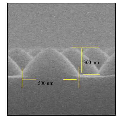
Fig. 1.
AnSEM image of the NPSS.
SEMICONDUCTOR MATERIALS
Jing Kong1, 2, , Meixin Feng1, Jin Cai1, Hui Wang1, Huaibing Wang1 and Hui Yang1
Corresponding author: Jing Kong, E-mail: jkong2013@sinano.ac.cn
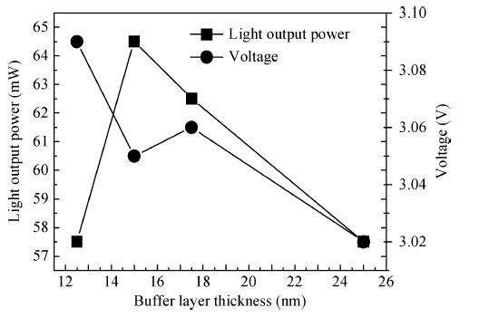
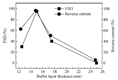
Abstract: High-quality gallium nitride (GaN) film was grown on nano-patterned sapphire substrates (NPSS) and investigated using XRD and SEM. It was found that the optimum thickness of the GaN buffer layer on the NPSS is 15 nm, which is thinner than that on micro-patterned sapphire substrates (MPSS). An interesting phenomenon was observed for GaN film grown on NPSS:GaN mainly grows on the trench regions and little grows on the sidewalls of the patterns at the initial growth stage, which is dramatically different from GaN grown on MPSS. In addition, the electrical and optical properties of LEDs grown on NPSS were characterized.
Key words: GaN, nano-patterned sapphires (NPSS), LED, two-step growth process
| [1] | |
| [2] | |
| [3] | |
| [4] | |
| [5] | |
| [6] | |
| [7] | |
| [8] | |
| [9] | |
| [10] | |
| [11] | |
| [12] | |
| [13] | |
| [14] | |
| [15] | |
| [16] |

| [1] | |
| [2] | |
| [3] | |
| [4] | |
| [5] | |
| [6] | |
| [7] | |
| [8] | |
| [9] | |
| [10] | |
| [11] | |
| [12] | |
| [13] | |
| [14] | |
| [15] | |
| [16] |


Article views: 2428 Times PDF downloads: 32 Times Cited by: 0 Times
Received: 13 October 2014 Revised: Online: Published: 01 April 2015
| Citation: |
Jing Kong, Meixin Feng, Jin Cai, Hui Wang, Huaibing Wang, Hui Yang. GaN grown on nano-patterned sapphire substrates[J]. Journal of Semiconductors, 2015, 36(4): 043003. doi: 10.1088/1674-4926/36/4/043003
J Kong, M X Feng, J Cai, H Wang, H B Wang, H Yang. GaN grown on nano-patterned sapphire substrates[J]. J. Semicond., 2015, 36(4): 043003. doi: 10.1088/1674-4926/36/4/043003.
Export: BibTex EndNote

|
| [1] | |
| [2] | |
| [3] | |
| [4] | |
| [5] | |
| [6] | |
| [7] | |
| [8] | |
| [9] | |
| [10] | |
| [11] | |
| [12] | |
| [13] | |
| [14] | |
| [15] | |
| [16] |

 WeChat ID
Journal of Semiconductors © 2017 All Rights Reserved 京ICP备05085259号-2

 DownLoad:

