


Fig. 1.
(a) X-ray pattern of ZnO films grown at $T_{\rm s}$ ranging within 250-400 $^\circ C$. (b) X-ray pattern of ZnO-IZO films grown at 350 $^\circ C$. JCPDS card of (002) orientation is shown by the solid line.
SEMICONDUCTOR MATERIALS
M. Benhaliliba1, A. Tiburcio-Silver2, A. Avila-Garcia3, A. Tavira3, Y. S. Ocak4, M. S. Aida5 and C. E. Benouis1
Corresponding author: M. Benhaliliba, E-mail: mbenhaliliba@gmail.com
Abstract: We synthesized the pure and indium-doped (IZO) ZnO films with a facile composition control spray pyrolysis route. The substrate temperature (Ts) and In-doping effects on the properties of as-grown films are investigated. The X-ray pattern confirms that the as-synthesized ZnO phase is grown along a (002) preferential plane. It is revealed that the crystalline structure is improved with a substrate temperature of 350 ℃. Moreover, the morphology of as-grown films, analyzed by AFM, shows nanostructures that have grown along the c-axis. The (3 × 3μm2) area scanned AFM surface studies give the smooth film surface RMS <40 nm. The UV-VIS-IR measurements reveal that the sprayed films are highly transparent in the visible and IR bands. The photoluminescence analysis shows that the strong blue and yellow luminescences of 2.11 and 2.81 eV are emitted from ZnO and IZO films with a slight shift in photon energy caused by In-doping. The band gap is a bit widened by In-doping, 3.21 eV (ZnO) and 3.31 eV (IZO) and the resistivity is reduced from 385 to 8 Ω ·m. An interesting result is the resistivity linear dependence on the substrate temperature of pure ZnO films.
Key words: sprayed ZnO films, deposition temperature, AFM observation, photoluminescence emission, resistivity
| [1] | |
| [2] | |
| [3] | |
| [4] | |
| [5] | |
| [6] | |
| [7] | |
| [8] | |
| [9] | |
| [10] | |
| [11] | |
| [12] | |
| [13] | |
| [14] | |
| [15] | |
| [16] | |
| [17] | |
| [18] | |
| [19] | |
| [20] | |
| [21] | |
| [22] |
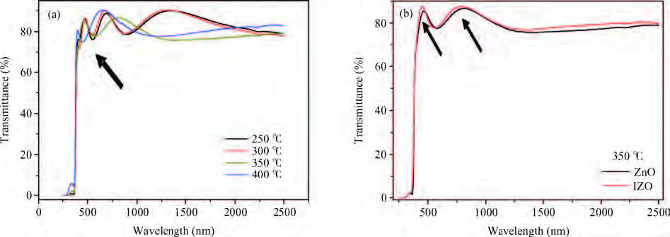


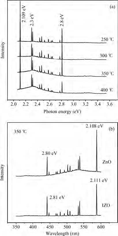
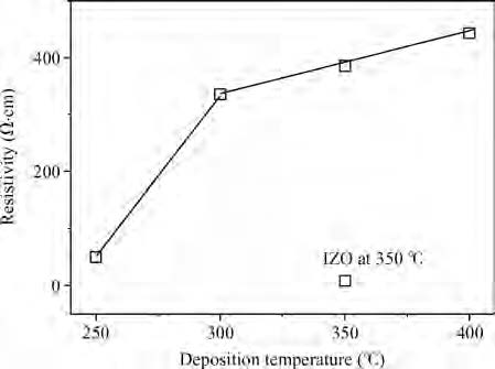
Table 1. RMS,height of grain,layer thickness,transmittance @ 550 nm,optical band gap and electrical parameters of sprayed ZnO and IZO films at various $T_{\rm s}$.
 DownLoad: CSV
| [1] | |
| [2] | |
| [3] | |
| [4] | |
| [5] | |
| [6] | |
| [7] | |
| [8] | |
| [9] | |
| [10] | |
| [11] | |
| [12] | |
| [13] | |
| [14] | |
| [15] | |
| [16] | |
| [17] | |
| [18] | |
| [19] | |
| [20] | |
| [21] | |
| [22] |


Article views: 2642 Times PDF downloads: 22 Times Cited by: 0 Times
Received: 26 January 2015 Revised: Online: Published: 01 August 2015
| Citation: |
M. Benhaliliba, A. Tiburcio-Silver, A. Avila-Garcia, A. Tavira, Y. S. Ocak, M. S. Aida, C. E. Benouis. The sprayed ZnO films: nanostructures and physical parameters[J]. Journal of Semiconductors, 2015, 36(8): 083001. doi: 10.1088/1674-4926/36/8/083001
M. Benhaliliba, A. Tiburcio-Silver, A. Avila-Garcia, A. Tavira, Y. S. Ocak, M. S. Aida, C. E. Benouis. The sprayed ZnO films: nanostructures and physical parameters[J]. J. Semicond., 2015, 36(8): 083001. doi: 10.1088/1674-4926/36/8/083001.
Export: BibTex EndNote

|
| [1] | |
| [2] | |
| [3] | |
| [4] | |
| [5] | |
| [6] | |
| [7] | |
| [8] | |
| [9] | |
| [10] | |
| [11] | |
| [12] | |
| [13] | |
| [14] | |
| [15] | |
| [16] | |
| [17] | |
| [18] | |
| [19] | |
| [20] | |
| [21] | |
| [22] |

 WeChat ID
Journal of Semiconductors © 2017 All Rights Reserved 京ICP备05085259号-2


