


Fig. 1.
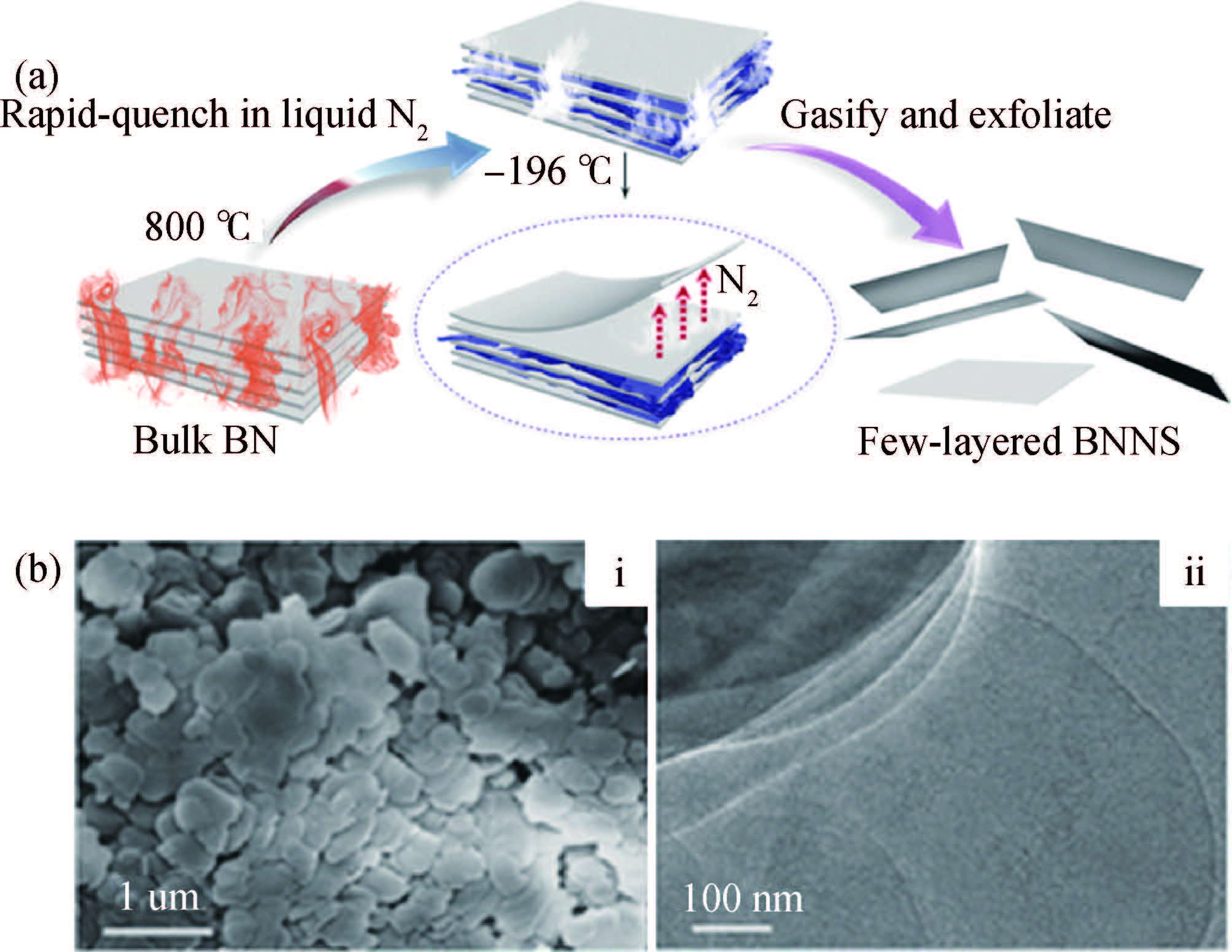
(Color online) (a) Schematic of the gas exfoliation of h-BN triggered by thermal expansion. (b) Characterization of exfoliated h-BN nanosheets: (i) SEM and (ii) TEM images after ten repeated cycles [28] .
SPECIAL TOPIC ON 2D MATERIALS AND DEVICES
Huihui Yang1, 2, 3, Feng Gao1, 2, 3, Mingjin Dai1, 2, 3, Dechang Jia1, Yu Zhou1 and Ping'an Hu1, 2, 3
Abstract: Two-dimensional (2D) layered materials, such as graphene, hexagonal boron nitride (h-BN), molybdenum disulfide (MoS2), have attracted tremendous interest due to their atom-thickness structures and excellent physical properties. h-BN has predominant advantages as the dielectric substrate in FET devices due to its outstanding properties such as chemically inert surface, being free of dangling bonds and surface charge traps, especially the large-band-gap insulativity. h-BN involved vertical heterostructures have been widely exploited during the past few years. Such heterostructures adopting h-BN as dielectric layers exhibit enhanced electronic performance, and provide further possibilities for device engineering. Besides, a series of intriguing physical phenomena are observed in certain vertical heterostructures, such as superlattice potential induced replication of Dirac points, band gap tuning, Hofstadter butterfly states, gate-dependent pseudospin mixing. Herein we focus on the rapid developments of h-BN synthesis and fabrication of vertical heterostructures devices based on h-BN, and review the novel properties as well as the potential applications of the heterostructures composed of h-BN.
Key words: h-BN, heterostructures, graphene, van der Waals epitaxy, FETs
| [1] |
Pakde A, Bando Y, Golberg D. Nano boron nitride flatland. Chem Soc Rev, 2014, 43:934 doi: 10.1039/C3CS60260E
|
| [2] |
Watanabe K, Taniguchi T, Kanda H. Direct-bandgap properties and evidence for ultraviolet lasing of hexagonal boron nitride single crystal. Nat Mater, 2004, 3(6):404 doi: 10.1038/nmat1134
|
| [3] |
Wang H L, Zhang X W, Liu H, et al. Synthesis of large-sized single-crystal hexagonal boron nitride domains on nickel foils by ion beam sputtering deposition. Adv Mater, 2015, 27(48):8109 doi: 10.1002/adma.201504042
|
| [4] |
Ahmed K, Dahal R, Weltz A, et al. Growth of hexagonal boron nitride on (111) Si for deep UV photonics and thermal neutron detection. Appl Phys Lett, 2016, 109(11):113501 doi: 10.1063/1.4962831
|
| [5] |
Yin J, Li J D, Hang Y, et al. Boron nitride nanostructures:fabrication, functionalization and applications. Small, 2016, 12(22):2942 doi: 10.1002/smll.201600053
|
| [6] |
Britnell L, Gorbachev R V, Jalil R, et al. Field-effect tunneling transistor based on vertical graphene heterostructures. Science, 2012, 335(6071):947 doi: 10.1126/science.1218461
|
| [7] |
Dean C R, Young A F, Meric I, et al. Boron nitride substrates for high-quality graphene electronics. Nat Nanotechnol, 2010, 5:722 doi: 10.1038/nnano.2010.172
|
| [8] |
Li L K, Ye G J, Tran V, et al. Quantum oscillations in a twodimensional electron gas in black phosphorus thin films. Nat Nanotechnol, 2015, 10:608 doi: 10.1038/nnano.2015.91
|
| [9] |
Giovannetti G, Khomyakov P A, Brocks G, et al. Substrateinduced band gap in graphene on hexagonal boron nitride:ab initio density functional calculations. Phys Rev B, 2007, 76(7):073103 doi: 10.1103/PhysRevB.76.073103
|
| [10] |
Yang W, Chen G R, Shi Z W, et al. Epitaxial growth of singledomain graphene on hexagonal boron nitride. Nat Mater, 2013, 12:792 doi: 10.1038/nmat3695
|
| [11] |
Wang E, Lu X B, Ding S J, et al. Gaps induced by inversion symmetry breaking and second-generation Dirac cones in graphene/hexagonal boron nitride. Nat Phys, 2016, 12:1111 doi: 10.1038/nphys3856
|
| [12] |
Yankowitz M, Xue J M, Cormode D, et al. Emergence of superlattice Dirac points in graphene on hexagonal boron nitride. Nat Phys, 2012, 8:382 doi: 10.1038/nphys2272
|
| [13] |
Ponomarenko L A, Gorbachev R V, Yu G L, et al. Cloning of Dirac fermions in graphene superlattices. Nature, 2013, 497:594 doi: 10.1038/nature12187
|
| [14] |
Gorbachev R V, Song J C W, Yu G L, et al. Detecting topological currents in graphene superlattices. Science, 2014, 346(6208):448 doi: 10.1126/science.1254966
|
| [15] |
Novoselov K S, Jiang D, Schedin F, et al. Two-dimensional atomic crystals. Proc Natl Acad Sci USA, 2005, 102(30):10451 doi: 10.1073/pnas.0502848102
|
| [16] |
Pacilé D, Meyer J C, Girit Ç Ö, et al. The two-dimensional phase of boron nitride:few-atomic-layer sheets and suspended membranes. Appl Phys Lett, 2008, 92(13):133107 doi: 10.1063/1.2903702
|
| [17] |
Alem N, Erni R, Kisielowski C, et al. Atomically thin hexagonal boron nitride probed by ultrahigh-resolution transmission electron microscopy. Phys Rev B, 2009, 80(15):155425 doi: 10.1103/PhysRevB.80.155425
|
| [18] |
Jin C H, Lin F, Suenaga K, et al. Fabrication of a freestanding boron nitride single layer and its defect assignments. Phys Rev Lett, 2009, 102(19):195505 doi: 10.1103/PhysRevLett.102.195505
|
| [19] |
Lee C G, Li Q Y, Kalb W, et al. Frictional characteristics of atomically thin sheets. Science, 2010, 328(5974):76 doi: 10.1126/science.1184167
|
| [20] |
Gorbachev R V, Riaz I, Nair R R, et al. Hunting for monolayer boron nitride:optical and Raman signatures. Small, 2011, 7(4):465 doi: 10.1002/smll.201001628
|
| [21] |
Golberg D, Bando Y, Huang Y, et al. Boron nitride nanotubes and nanosheets. ACS Nano, 2010, 4(6):2979 doi: 10.1021/nn1006495
|
| [22] |
Zhi C Y, Bando Y, Tang C C, et al. Large-scale fabrication of boron nitride nanosheets and their utilization in polymeric composites with improved thermal and mechanical properties. Adv Mater, 2009, 21(28):2889 doi: 10.1002/adma.v21:28
|
| [23] |
Lin Y, Williams T V, Connell J W. Soluble, exfoliated hexagonal boron nitride nanosheets. J Phys Chem Lett, 2010, 1(1):277 doi: 10.1021/jz9002108
|
| [24] |
Wang Y, Shi Z X, Yin J. Boron nitride nanosheets:large-scale exfoliation in methanesulfonic acid and their composites with polybenzimidazole. J Mater Chem, 2011, 21:11371 doi: 10.1039/c1jm10342c
|
| [25] |
Lin Y, Williams T V, Xu T B, et al. Aqueous dispersions of fewlayered and monolayered hexagonal boron nitride nanosheets from sonication-assisted hydrolysis:critical role of water. J Phys Chem, 2011, 115:2679 doi: 10.1021/jp1105778
|
| [26] |
Zhou K G, Mao N N, Wang H X, et al. A mixed-solvent strategy for efficient exfoliation of inorganic graphene analogues. Angew Chem Int Edit, 2011, 50(46):10839 doi: 10.1002/anie.v50.46
|
| [27] |
Sarmazdeh Z R, Jafari S H, Ahmadi S J, et al. Large-scale exfoliation of hexagonal boron nitride with combined fast quenching and liquid exfoliation strategies. J Mater Sci, 2016, 51(6):3162 doi: 10.1007/s10853-015-9626-4
|
| [28] |
Zhu W S, Gao X, Li Q, et al. Controlled gas exfoliation of boron nitride into few-layered nanosheets. Angew Chem Int Edit, 2016, 128:10924 doi: 10.1002/ange.201605515
|
| [29] |
Nagashima A, Tejima N, Gamou Y, et al. Electronic dispersion relations of monolayer hexagonal boron nitride formed on the Ni(111) surface. Phys Rev B, 1995, 51(7):4606 doi: 10.1103/PhysRevB.51.4606
|
| [30] |
Koepke J C, Wood J D, Chen Y F, et al. Role of pressure in the growth of hexagonal boron nitride thin films from ammoniaborane. Chem Mater, 2016, 28(12):4169 doi: 10.1021/acs.chemmater.6b00396
|
| [31] |
Auwärter W, Suter H U, Sachdev H, et al. Synthesis of one monolayer of hexagonal boron nitride on Ni(111) from BTrichloroborazine (ClBNH)3. Chem Mater, 2004, 16(2):343 doi: 10.1021/cm034805s
|
| [32] |
Müller F, Stöwe K, Sachdev H. Symmetry versus commensurability:epitaxial growth of hexagonal boron nitride on Pt(111) from B-Trichloroborazine (ClBNH)3. Chem Mater, 2005, 17(13):3464 doi: 10.1021/cm048629e
|
| [33] |
Shi Y M, Hamsen C, Jia X T, et al. Synthesis of few-layer hexagonal boron nitride thin film by chemical vapor deposition. Nano Lett, 2010, 10(10):4134 doi: 10.1021/nl1023707
|
| [34] |
Song L, Ci L J, Lu H, et al. Large scale growth and characterization of atomic hexagonal boron nitride layers. Nano Lett, 2010, 10(8):3209 doi: 10.1021/nl1022139
|
| [35] |
Lee K H, Shin H J, Lee J, et al. Large-scale synthesis of high-quality hexagonal boron nitride nanosheets for large-area graphene electronics. Nano Lett, 2012, 12(1):714 doi: 10.1021/nl203635v
|
| [36] |
Gao Y, Ren W C, Ma T, et al. Repeated and controlled growth of monolayer, bilayer and few-layer hexagonal boron nitride on Pt foils. ACS Nano, 2013, 7(6):5200 https://www.researchgate.net/profile/Hui-Ming_Cheng/publication/236688944_Repeated_and_Controlled_Growth_of_Monolayer_Bilayer_and_Few-Layer_Hexagonal_Boron_Nitride_on_Pt_Foils/links/561f444808aecade1acd2ecc.pdf?inViewer=true&pdfJsDownload=true&disableCoverPage=true&origin=publication_detail
|
| [37] |
Ismach A, Chou H, Ferrer D A, et al. Toward the controlled synthesis of hexagonal boron nitride films. ACS Nano, 2012, 6(7):6378 doi: 10.1021/nn301940k
|
| [38] |
Chatterjee S, Luo Z T, Acerce M, et al. Chemical vapor deposition of boron nitride nanosheets on metallic substrates via decaborane/ammonia reactions. Chem Mater, 2011, 23(20):4414 doi: 10.1021/cm201955v
|
| [39] |
Kim K K, Hsu A, Jia X T, et al. Synthesis of monolayer hexagonal boron nitride on Cu foil using chemical vapor deposition. Nano Lett, 2012, 12(1):162 doi: 10.1021/nl203249a
|
| [40] |
Behura S J, Nguyen P, Che S W, et al. Large-area, transferfree, oxide-assisted synthesis of hexagonal boron nitride films and their heterostructures with MoS2 and WS2. J Am Chem Soc, 2015, 137(40):13060 doi: 10.1021/jacs.5b07739
|
| [41] |
Han J H, Lee J Y, Kwon H M, et al. Synthesis of waferscale hexagonal boron nitride monolayers free of aminoborane nanoparticles by chemical vapor deposition. Nanotechnology, 2014, 25(14):145604 doi: 10.1088/0957-4484/25/14/145604
|
| [42] |
Morsche M, Corso M, Greber T, et al. Formation of single layer h-BN on Pd(111). Surf Sci, 2006, 600(16):3280 doi: 10.1016/j.susc.2006.06.016
|
| [43] |
Müller F, Hüfner S, Sachdev H, et al. Epitaxial growth of hexagonal boron nitride on Ag(111). Phys Rev B, 2010, 82(11):113406 doi: 10.1103/PhysRevB.82.113406
|
| [44] |
Müller F, Hüfner S, Sachdev H. One-dimensional structure of boron nitride on chromium (110)-a study of the growth of boron nitride by chemical vapour deposition of borazine. Surf Sci, 2008, 602(22):3467 doi: 10.1016/j.susc.2008.06.037
|
| [45] |
Corso M, Greber T, Osterwalder J. H-BN on Pd(110):a tunable system for self-assembled nanostructures. Surf Sci, 2005, 577(2/3):78 https://www.researchgate.net/publication/239169796_H-BN_on_Pd1_1_0_A_tunable_system_for_self-assembled_nanostructures
|
| [46] |
Goriachko A, He Y B, Knapp M, et al. Self-assembly of a hexagonal boron nitride nanomesh on Ru(0001). Langmuir, 2007, 23:2928 doi: 10.1021/la062990t
|
| [47] |
Tay R Y, Griep M H, Mallick G, et al. Growth of large singlecrystalline two-dimensional boron nitride hexagons on electropolished copper. Nano Lett, 2014, 14(2):839 doi: 10.1021/nl404207f
|
| [48] |
Wang L F, Wu B, Chen J, et al. Monolayer hexagonal boron nitride films with large domain size and clean interface for enhancing the mobility of graphene-based field-effect transistors. Adv Mater, 2014, 26(10):1559 doi: 10.1002/adma.201304937
|
| [49] |
Wang J, Chen L F, Wu N, et al. Graphene on liquid metal by chemical vapour deposition at reduced temperature. Carbon, 2016, 96:799 doi: 10.1016/j.carbon.2015.10.015
|
| [50] |
Geng D C, Wu B, Guo Y L, et al. Uniform hexagonal graphene flakes and films grown on liquid copper surface. Proc Natl Acad Sci USA, 2012, 109(21):17992 https://www.researchgate.net/publication/224052905_Uniform_hexagonal_graphene_flakes_and_films_grown_on_liquid_copper_surface
|
| [51] |
Tan L F, Han J L, Mendes R G, et al. Self-aligned singlecrystalline hexagonal boron nitride arrays:toward higher integrated electronic devices. Adv Electron Mater, 2015, 1(11):1500223 doi: 10.1002/aelm.201500223
|
| [52] |
Khan M H, Huang Z G, Xiao F, et al. Synthesis of large and few atomic layers of hexagonal boron nitride on melted copper. Sci Rep, 2015, 5:7743 doi: 10.1038/srep07743
|
| [53] |
Jang A R, Hong S, Hyun C, et al. Wafer-scale and wrinkle-free epitaxial growth of single-orientated multilayer hexagonal boron nitride on sapphire. Nano Lett, 2016, 16(5):3360 doi: 10.1021/acs.nanolett.6b01051
|
| [54] |
Caneva S, Weatherup R S, Bayer B C, et al. Nucleation control for large, single crystalline domains of monolayer hexagonal boron nitride via Si-doped Fe catalysts. Nano Lett, 2015, 15(3):1867 doi: 10.1021/nl5046632
|
| [55] |
Lu G Y, Wu T R, Yuan Q H, et al. Synthesis of large singlecrystal hexagonal boron nitride grains on Cu-Ni alloy. Nat Commun, 2015, 6:6160 doi: 10.1038/ncomms7160
|
| [56] |
Li J, Wang X Y, Liu X R, et al. Facile growth of centimeter-sized single-crystal graphene on copper foil at atmospheric pressure. J Mater Chem C, 2015, 3:3530 doi: 10.1039/C5TC00235D
|
| [57] |
Guo W, Jing F, Xiao J, et al. Oxidative-etching-assisted synthesis of centimeter-sized single-crystalline graphene. Adv Mater, 2016, 28(16):3152 doi: 10.1002/adma.201503705
|
| [58] |
Tay R Y, Park H J, Ryu G H, et al. Synthesis of aligned symmetrical multifaceted monolayer hexagonal boron nitride single crystals on resolidified copper. Nanoscale, 2016, 8(4):2434 doi: 10.1039/C5NR08036C
|
| [59] |
Wu Q K, Park J H, Park S, et al. Single crystalline film of hexagonal boron nitride atomic monolayer by controlling nucleation seeds and domains. Sci Rep, 2015, 5:16159 doi: 10.1038/srep16159
|
| [60] |
Stehle Y, Meyerlll H M, Unocic R R, et al. Synthesis of hexagonal boron nitride monolayer:control of nucleation and crystal morphology. Chem Mater, 2015, 27(23):8041 doi: 10.1021/acs.chemmater.5b03607
|
| [61] |
Yin J, Yu J, Li X M, et al. Large single-crystal hexagonal boron nitride monolayer domains with controlled morphology and straight merging boundaries. Small, 2015, 11(35):4497 doi: 10.1002/smll.v11.35
|
| [62] |
Zhang Z H, Liu Y Y, Yang Y, et al. Growth mechanism and morphology of hexagonal boron nitride. Nano Lett, 2016, 16(2):1398 doi: 10.1021/acs.nanolett.5b04874
|
| [63] |
Song X J, Gao J F, Nie Y F, et al. Chemical vapor deposition growth of large-scale hexagonal boron nitride with controllable orientation. Nano Res, 2015, 8(10):3164 doi: 10.1007/s12274-015-0816-9
|
| [64] |
Wood G E, Marsden A J, Mudd J J, et al. van der Waals epitaxy of monolayer hexagonal boron nitride on copper foil:growth, crystallography and electronic band structure. 2D Mater, 2015, 2(2):025003 doi: 10.1088/2053-1583/2/2/025003
|
| [65] |
Li J D, Li Y, Yin J, et al. Growth of polar hexagonal boron nitride monolayer on nonpolar copper with unique orientation. Small, 2016, 12(27):3645 doi: 10.1002/smll.v12.27
|
| [66] |
Sutter P, Lahiri J, Albrecht P, et al. Chemical vapor deposition and etching of high-quality monolayer hexagonal boron nitride films. ACS Nano, 2011, 5(9):7303 doi: 10.1021/nn202141k
|
| [67] |
Wang L F, Wu B, Jiang L L, et al. Growth and etching of monolayer hexagonal boron nitride. Adv Mater, 2015, 27(330):4858 https://www.researchgate.net/publication/280118233_Growth_and_Etching_of_Monolayer_Hexagonal_Boron_Nitride
|
| [68] |
Sharma S, Kalita G, Vishwakarma R, et al. Opening of triangular hole in triangular-shaped chemical vapor deposited hexagonal boron nitride crystal. Sci Rep, 2015, 5:10426 doi: 10.1038/srep10426
|
| [69] |
Elbadawi C, Tran T T, Kolíbal M, et al. Electron beam directed etching of hexagonal boron nitride. Nanoscale, 2016, 8:16182 doi: 10.1039/C6NR04959A
|
| [70] |
Kan M, Zhou J, Wang Q, et al. Tuning the band gap and magnetic properties of BN sheets impregnated with graphene flakes. Phys Rev B, 2011, 84(20):205412 doi: 10.1103/PhysRevB.84.205412
|
| [71] |
Ci L J, Song L, Jin C H, et al. Atomic layers of hybridized boron nitride and graphene domains. Nat Mater, 2010, 9:430 doi: 10.1038/nmat2711
|
| [72] |
Levendorf M P, Kim C J, Brown L, et al. Graphene and boron nitride lateral heterostructures for atomically thin circuitry. Nature, 2012, 488:627 doi: 10.1038/nature11408
|
| [73] |
Liu Z, Ma L L, Shi G, et al. In-plane heterostructures of graphene and hexagonal boron nitride with controlled domain sizes. Nat Nanotechnol, 2013, 8:119 doi: 10.1038/nnano.2012.256
|
| [74] |
Liu L, Park J, Siegel D A, et al. Heteroepitaxial growth of twoDimensional Hexagonal boron nitride templated by graphene edges. Science, 2014, 343(6167):163 doi: 10.1126/science.1246137
|
| [75] |
Han G H, Rodríguez-Manzo J A, Lee C W, et al. Continuous growth of hexagonal graphene and boron nitride in-plane heterostructures by atmospheric pressure chemical vapor deposition. ACS Nano, 2013, 7(11):10129 doi: 10.1021/nn404331f
|
| [76] |
Sutter P, Cortes R, Lahiri J, et al. Interface formation in monolayer graphene-boron nitride heterostructures. Nano Lett, 2012, 12(9):4869 doi: 10.1021/nl302398m
|
| [77] |
Gao Y B, Zhang Y F, Chen P C, et al. Toward single-layer uniform hexagonal boron nitride-graphene patchworks with zigzag linking edge. Nano Lett, 2013, 13(7):3439 doi: 10.1021/nl4021123
|
| [78] |
Gao T, Song X J, Du H W, et al. Temperature-triggered chemical switching growth of in-plane and vertically stacked grapheneboron nitride heterostructures. Nat Commun, 2015, 6:6835 doi: 10.1038/ncomms7835
|
| [79] |
Ceballos F, Bellus M Z, Chiu H Y, et al. Ultrafast charge separation and indirect exciton formation in a MoS2-MoSe2 van der Waals heterostructure. ACS Nano, 2014, 8(12):12717 doi: 10.1021/nn505736z
|
| [80] |
Bellus M Z, Ceballos F, Chiu H Y, et al. Tightly bound trions in transition metal dichalcogenide heterostructures. ACS Nano, 2015, 9(6):6459 doi: 10.1021/acsnano.5b02144
|
| [81] |
Son M, Lim H, Hong M, et al. Direct growth of graphene pad on exfoliated hexagonal boron nitride surface. Nanoscale, 2011, 3:3089 doi: 10.1039/c1nr10504c
|
| [82] |
Tang S J, Ding G Q, Xie X M, et al. Nucleation and growth of single crystal graphene on hexagonal boron nitride. Carbon, 2011, 50(1):329 https://www.researchgate.net/publication/256677412_Nucleation_and_growth_of_single_crystal_graphene_on_hexagonal_boron_nitride
|
| [83] |
Tang S J, Wang H M, Zhang Y, et al. Precisely aligned graphene grown on hexagonal boron nitride by catalyst free chemical vapor deposition. Sci Rep, 2013, 3:2666 http://www.oalib.com/paper/3401588
|
| [84] |
Mishra N, Miseikis V, Convertino D, et al. Rapid and catalystfree van der Waals epitaxy of graphene on hexagonal boron nitride. Carbon, 2016, 96:497 doi: 10.1016/j.carbon.2015.09.100
|
| [85] |
Tang S J, Wang H M, Wang H S, et al. Silane-catalysed fast growth of large single-crystalline graphene on hexagonal boron nitride. Nat Commun, 2015, 6:6499 doi: 10.1038/ncomms7499
|
| [86] |
Kim S M, Hsu A, Araujo P T, et al. Synthesis of patched or stacked graphene and hBN flakes:a route to hybrid structure discovery. Nano Lett, 2013, 13(3):933 doi: 10.1021/nl303760m
|
| [87] |
Meng J H, Zhang X W, Wang H L, et al. Synthesis of in-plane and stacked graphene/hexagonal boron nitride heterostructures by combining with ion beam sputtering deposition and chemical vapor deposition. Nanoscale, 2015, 7:16046 doi: 10.1039/C5NR04490A
|
| [88] |
Gong Y J, Lei S D, Ye G L, et al. Two-step growth of twodimensional WSe2/MoSe2 heterostructures. Nano Lett, 2015, 15(9):6135 doi: 10.1021/acs.nanolett.5b02423
|
| [89] |
Zhang C H, Zhao S L, Jin C H, et al. Direct growth of large-area graphene and boron nitride heterostructures by a co-segregation method. Nat Commun, 2015, 6:6519 doi: 10.1038/ncomms7519
|
| [90] |
Song X J, Gao T, Nie Y F, et al. Seed-assisted growth of singlecrystalline patterned graphene domains on hexagonal boron nitride by chemical vapor deposition. Nano Lett, 2016, 16(10):6109 doi: 10.1021/acs.nanolett.6b02279
|
| [91] |
Zhang Y, Zhang Y F, Ji Q Q, et al. Controlled growth of highquality monolayer WS2 layers on sapphire and imaging its grain boundary. ACS Nano, 2013, 7(10):8963 doi: 10.1021/nn403454e
|
| [92] |
Zhan Y J, Liu Z, Najmaei S, et al. Large-area vapor-phase growth and characterization of MoS2 atomic layers on a SiO2 substrate. Small, 2012, 8(7):966 doi: 10.1002/smll.201102654
|
| [93] |
Wang X L, Gong Y J, Shi G, et al. Chemical vapor deposition growth of crystalline monolayer MoSe2. ACS Nano, 2014, 8(5):5125 doi: 10.1021/nn501175k
|
| [94] |
Cui X, Lee G H, Kim Y D, et al. Multi-terminal transport measurements of MoS2 using a van der Waals heterostructure device platform. Nat Nanotechnol, 2015, 10:534 doi: 10.1038/nnano.2015.70
|
| [95] |
Lee G H, Yu Y J, Cui X, et al. Flexible and transparent MoS2 field-effect transistors on hexagonal boron nitride-graphene heterostructures. ACS Nano, 2013, 7(9):7931 doi: 10.1021/nn402954e
|
| [96] |
Ross J S, Klement P, Jones A M, et al. Electrically tunable excitonic light-emitting diodes based on monolayer WSe2 p-n junctions. Nat Nanotechnol, 2014, 9:268 doi: 10.1038/nnano.2014.26
|
| [97] |
Okada M, Sawazaki T, Watanabe K, et al. Direct chemical vapor deposition growth of WS2 atomic layers on hexagonal boron nitride. ACS Nano, 2014, 8(8):8273 doi: 10.1021/nn503093k
|
| [98] |
Yan A, Velasco J Jr, Kahn S, et al. Direct growth of single- and few-layer MoS2 on h-BN with preferred relative rotation angles. Nano Lett, 2015, 15(10):6324 doi: 10.1021/acs.nanolett.5b01311
|
| [99] |
Wang S S, Wang X C, Warner J H. All chemical vapor deposition growth of MoS2:h-BN vertical van der Waals heterostructures. ACS Nano, 2015, 9(5):5246 doi: 10.1021/acsnano.5b00655
|
| [100] |
Fu L, Sun Y Y, Wu N, et al. Direct growth of MoS2/h-BN heterostructures via a sulfide-resistant alloy. ACS Nano, 2016, 10(2):2063 doi: 10.1021/acsnano.5b06254
|
| [101] |
Zhang M, Zhu Y M, Wang X S, et al. Controlled synthesis of ZrS2 monolayer and few layers on hexagonal boron nitride. Nat Nanotechnol, 2015, 10:534 doi: 10.1038/nnano.2015.70
|
| [102] |
Woods C R, Britnell L, Eckmann A, et al. Commensurateincommensurate transition in graphene on hexagonal boron nitride. Nat Phys, 2014, 10:451 doi: 10.1038/nphys2954
|
| [103] |
Park C H, Yang L, Son Y W, et al. New generation of massless Dirac fermions in graphene under external periodic potentials. Phys Rev Lett, 2008, 101(12):126804 doi: 10.1103/PhysRevLett.101.126804
|
| [104] |
Sui M Q, Chen G R, Ma L G, et al. Gate-tunable topological valley transport in bilayer graphene. Nat Phys, 2015, 11:1027 doi: 10.1038/nphys3485
|
| [105] |
Shi Z W, Jin C H, Yang W, et al. Gate-dependent pseudospin mixing in graphene/boron nitride moiré superlattices. Nat Phys, 2014, 10:743
|
| [106] |
Hunt B, Sanchez-Yamagishi J D, Young A F, et al. Massive Dirac Fermions and Hofstadter butterfly in a van der Waals heterostructures. Science, 2013, 340(6139):1427 doi: 10.1126/science.1237240
|
| [107] |
Yu G L, Gorbachev R V, Tu J S, et al. Hierarchy of Hofstadter states and replica quantum Hall ferromagnetism in graphene superlattices. Nat Phys, 2014, 10:525 doi: 10.1038/nphys2979
|
| [108] |
Xue J M, Yamagishi J S, Bulmash D, et al. Scanning tunnelling microscopy and spectroscopy of ultra-flat graphene on hexagonal boron nitride. Nat Mater, 2011, 10:282 doi: 10.1038/nmat2968
|
| [109] |
Petrone N, Chari T, Meric I, et al. Flexible graphene field-effect transistors encapsulated in hexagonal boron nitride. ACS Nano, 2015, 9(9):8953 doi: 10.1021/acsnano.5b02816
|
| [110] |
Iqbal M W, Iqbal M Z, Khan M F, et al. High-mobility and airstable single-layer WS2 field-effect transistors sandwiched between chemical vapor deposition-grown hexagonal BN films. Sci Rep, 2015, 5:10699 doi: 10.1038/srep10699
|
| [111] |
Lee G H, Yu Y J, Cui X, et, al. Flexible and transparent MoS2 field-effect transistors on hexagonal boron nitride-graphene heterostructures. ACS Nano, 2013, 7(9):7931 doi: 10.1021/nn402954e
|
| [112] |
Chan M Y, Komatsu K, Li S L, et, al. Suppression of thermally activated carrier transport in atomically thin MoS2 on crystalline hexagonal boron nitride substrates. Nanoscale, 2013, 5:9572 doi: 10.1039/c3nr03220e
|
| [113] |
Wang L, Chen Z, Dean C R, et al. Negligible environmental sensitivity of graphene in a hexagonal boron nitride/graphene/h-BN sandwich structure. ACS Nano, 2012, 6(10):9314 doi: 10.1021/nn304004s
|
| [114] |
Stolyarov M A, Liu G X, Rumyantsev S L, et al. Suppression of 1=f noise in near-ballistic h-BN-graphene-h-BN heterostructure field-effect transistors. Appl Phys Lett, 2015, 107(2):023106 doi: 10.1063/1.4926872
|
| [115] |
Britnell L, Gorbachev R V, Jalil R, et al. Electron tunneling through ultrathin boron nitride crystalline barriers. Nano Lett, 2012, 12(3):1707 doi: 10.1021/nl3002205
|
| [116] |
Lee S H, Choi M S, Lee J, et al. High performance vertical tunneling diodes using graphene/hexagonal boron nitride/graphene hetero-structure. Appl Phys Lett, 2014, 104(5):053103 doi: 10.1063/1.4863840
|
| [117] |
Nguyen V H, Mazzamuto F, Bournel A, et al. Resonant tunnelling diodes based on graphene/h-BN heterostructure. J Phys D, 2012, 45:325104 doi: 10.1088/0022-3727/45/32/325104
|
| [118] |
Gaskell J, Eaves L, Novoselov K S, et al. Graphene-hexagonal boron nitride resonant tunneling diodes as high-frequency oscillators. Appl Phys Lett, 2015, 107(10):103105 doi: 10.1063/1.4930230
|
| [119] |
Menga J H, Liua X, Zhang X W, et al. Interface engineering for highly efficient graphene-on-silicon Schottky junction solar cells by introducing a hexagonal boron nitride interlayer. Nano Energy, 2016, 28:44 doi: 10.1016/j.nanoen.2016.08.028
|
| [120] |
Woessner A, Lundeberg M B, Gao Y D, et al. Highly confined low-loss plasmons in graphene-boron nitride heterostructures. Nat Mater, 2015, 14:421 http://theory.physics.lehigh.edu/rotkin/Personal/plasmon-polariton/Hillenbrand_%20Highly%20confined%20low-loss%20plasmons%20in%20graphene%e2%80%93boron%20nitride%20heterostructures%20_nmat4169.pdf
|
| [121] |
Ma Q, Andersen T I, Nair N L, et al. Tuning ultrafast electron thermalization pathways in a van der Waals heterostructures. Nat Phys, 2016, 12:455 doi: 10.1038/nphys3620
|
| [122] |
Chen C C, Li Z, Shi L, et al. Thermoelectric transport across graphene/hexagonal boron nitride/graphene heterostructures. Nano Res, 2015, 8(2):666 doi: 10.1007/s12274-014-0550-8
|
| [123] |
Xu Y, Guo Z D, Chen H B, et al. In-plane and tunneling pressure sensors based on graphene/hexagonal boron nitride heterostructures. Appl Phys Lett, 2011, 99(13):133109 doi: 10.1063/1.3643899
|
| [124] |
Dauber J, Sagade A A, Oellers M, et al. Ultra-sensitive Hall sensors based on graphene encapsulated in hexagonal boron nitride. Appl Phys Lett, 2015, 106(19):193501 doi: 10.1063/1.4919897
|
| [125] |
Gopinadhan K, Shin Y J, Jalil R, et al. Extremely large magnetoresistance in few-layer graphene/boron-nitride heterostructures. Nat Commun, 2015, 6:8337 doi: 10.1038/ncomms9337
|


Article views: 6158 Times PDF downloads: 75 Times Cited by: 0 Times
Received: 19 October 2016 Revised: 09 November 2016 Online: Published: 01 March 2017
| Citation: |
Huihui Yang, Feng Gao, Mingjin Dai, Dechang Jia, Yu Zhou, Ping'an Hu. Recent advances in preparation,properties and device applications of two-dimensional h-BN and its vertical heterostructures[J]. Journal of Semiconductors, 2017, 38(3): 031004. doi: 10.1088/1674-4926/38/3/031004
H H Yang, F Gao, M J Dai, D C Jia, Y Zhou, P A Hu. Recent advances in preparation,properties and device applications of two-dimensional h-BN and its vertical heterostructures[J]. J. Semicond., 2017, 38(3): 031004. doi: 10.1088/1674-4926/38/3/031004.
Export: BibTex EndNote

|
| [1] |
Pakde A, Bando Y, Golberg D. Nano boron nitride flatland. Chem Soc Rev, 2014, 43:934 doi: 10.1039/C3CS60260E
|
| [2] |
Watanabe K, Taniguchi T, Kanda H. Direct-bandgap properties and evidence for ultraviolet lasing of hexagonal boron nitride single crystal. Nat Mater, 2004, 3(6):404 doi: 10.1038/nmat1134
|
| [3] |
Wang H L, Zhang X W, Liu H, et al. Synthesis of large-sized single-crystal hexagonal boron nitride domains on nickel foils by ion beam sputtering deposition. Adv Mater, 2015, 27(48):8109 doi: 10.1002/adma.201504042
|
| [4] |
Ahmed K, Dahal R, Weltz A, et al. Growth of hexagonal boron nitride on (111) Si for deep UV photonics and thermal neutron detection. Appl Phys Lett, 2016, 109(11):113501 doi: 10.1063/1.4962831
|
| [5] |
Yin J, Li J D, Hang Y, et al. Boron nitride nanostructures:fabrication, functionalization and applications. Small, 2016, 12(22):2942 doi: 10.1002/smll.201600053
|
| [6] |
Britnell L, Gorbachev R V, Jalil R, et al. Field-effect tunneling transistor based on vertical graphene heterostructures. Science, 2012, 335(6071):947 doi: 10.1126/science.1218461
|
| [7] |
Dean C R, Young A F, Meric I, et al. Boron nitride substrates for high-quality graphene electronics. Nat Nanotechnol, 2010, 5:722 doi: 10.1038/nnano.2010.172
|
| [8] |
Li L K, Ye G J, Tran V, et al. Quantum oscillations in a twodimensional electron gas in black phosphorus thin films. Nat Nanotechnol, 2015, 10:608 doi: 10.1038/nnano.2015.91
|
| [9] |
Giovannetti G, Khomyakov P A, Brocks G, et al. Substrateinduced band gap in graphene on hexagonal boron nitride:ab initio density functional calculations. Phys Rev B, 2007, 76(7):073103 doi: 10.1103/PhysRevB.76.073103
|
| [10] |
Yang W, Chen G R, Shi Z W, et al. Epitaxial growth of singledomain graphene on hexagonal boron nitride. Nat Mater, 2013, 12:792 doi: 10.1038/nmat3695
|
| [11] |
Wang E, Lu X B, Ding S J, et al. Gaps induced by inversion symmetry breaking and second-generation Dirac cones in graphene/hexagonal boron nitride. Nat Phys, 2016, 12:1111 doi: 10.1038/nphys3856
|
| [12] |
Yankowitz M, Xue J M, Cormode D, et al. Emergence of superlattice Dirac points in graphene on hexagonal boron nitride. Nat Phys, 2012, 8:382 doi: 10.1038/nphys2272
|
| [13] |
Ponomarenko L A, Gorbachev R V, Yu G L, et al. Cloning of Dirac fermions in graphene superlattices. Nature, 2013, 497:594 doi: 10.1038/nature12187
|
| [14] |
Gorbachev R V, Song J C W, Yu G L, et al. Detecting topological currents in graphene superlattices. Science, 2014, 346(6208):448 doi: 10.1126/science.1254966
|
| [15] |
Novoselov K S, Jiang D, Schedin F, et al. Two-dimensional atomic crystals. Proc Natl Acad Sci USA, 2005, 102(30):10451 doi: 10.1073/pnas.0502848102
|
| [16] |
Pacilé D, Meyer J C, Girit Ç Ö, et al. The two-dimensional phase of boron nitride:few-atomic-layer sheets and suspended membranes. Appl Phys Lett, 2008, 92(13):133107 doi: 10.1063/1.2903702
|
| [17] |
Alem N, Erni R, Kisielowski C, et al. Atomically thin hexagonal boron nitride probed by ultrahigh-resolution transmission electron microscopy. Phys Rev B, 2009, 80(15):155425 doi: 10.1103/PhysRevB.80.155425
|
| [18] |
Jin C H, Lin F, Suenaga K, et al. Fabrication of a freestanding boron nitride single layer and its defect assignments. Phys Rev Lett, 2009, 102(19):195505 doi: 10.1103/PhysRevLett.102.195505
|
| [19] |
Lee C G, Li Q Y, Kalb W, et al. Frictional characteristics of atomically thin sheets. Science, 2010, 328(5974):76 doi: 10.1126/science.1184167
|
| [20] |
Gorbachev R V, Riaz I, Nair R R, et al. Hunting for monolayer boron nitride:optical and Raman signatures. Small, 2011, 7(4):465 doi: 10.1002/smll.201001628
|
| [21] |
Golberg D, Bando Y, Huang Y, et al. Boron nitride nanotubes and nanosheets. ACS Nano, 2010, 4(6):2979 doi: 10.1021/nn1006495
|
| [22] |
Zhi C Y, Bando Y, Tang C C, et al. Large-scale fabrication of boron nitride nanosheets and their utilization in polymeric composites with improved thermal and mechanical properties. Adv Mater, 2009, 21(28):2889 doi: 10.1002/adma.v21:28
|
| [23] |
Lin Y, Williams T V, Connell J W. Soluble, exfoliated hexagonal boron nitride nanosheets. J Phys Chem Lett, 2010, 1(1):277 doi: 10.1021/jz9002108
|
| [24] |
Wang Y, Shi Z X, Yin J. Boron nitride nanosheets:large-scale exfoliation in methanesulfonic acid and their composites with polybenzimidazole. J Mater Chem, 2011, 21:11371 doi: 10.1039/c1jm10342c
|
| [25] |
Lin Y, Williams T V, Xu T B, et al. Aqueous dispersions of fewlayered and monolayered hexagonal boron nitride nanosheets from sonication-assisted hydrolysis:critical role of water. J Phys Chem, 2011, 115:2679 doi: 10.1021/jp1105778
|
| [26] |
Zhou K G, Mao N N, Wang H X, et al. A mixed-solvent strategy for efficient exfoliation of inorganic graphene analogues. Angew Chem Int Edit, 2011, 50(46):10839 doi: 10.1002/anie.v50.46
|
| [27] |
Sarmazdeh Z R, Jafari S H, Ahmadi S J, et al. Large-scale exfoliation of hexagonal boron nitride with combined fast quenching and liquid exfoliation strategies. J Mater Sci, 2016, 51(6):3162 doi: 10.1007/s10853-015-9626-4
|
| [28] |
Zhu W S, Gao X, Li Q, et al. Controlled gas exfoliation of boron nitride into few-layered nanosheets. Angew Chem Int Edit, 2016, 128:10924 doi: 10.1002/ange.201605515
|
| [29] |
Nagashima A, Tejima N, Gamou Y, et al. Electronic dispersion relations of monolayer hexagonal boron nitride formed on the Ni(111) surface. Phys Rev B, 1995, 51(7):4606 doi: 10.1103/PhysRevB.51.4606
|
| [30] |
Koepke J C, Wood J D, Chen Y F, et al. Role of pressure in the growth of hexagonal boron nitride thin films from ammoniaborane. Chem Mater, 2016, 28(12):4169 doi: 10.1021/acs.chemmater.6b00396
|
| [31] |
Auwärter W, Suter H U, Sachdev H, et al. Synthesis of one monolayer of hexagonal boron nitride on Ni(111) from BTrichloroborazine (ClBNH)3. Chem Mater, 2004, 16(2):343 doi: 10.1021/cm034805s
|
| [32] |
Müller F, Stöwe K, Sachdev H. Symmetry versus commensurability:epitaxial growth of hexagonal boron nitride on Pt(111) from B-Trichloroborazine (ClBNH)3. Chem Mater, 2005, 17(13):3464 doi: 10.1021/cm048629e
|
| [33] |
Shi Y M, Hamsen C, Jia X T, et al. Synthesis of few-layer hexagonal boron nitride thin film by chemical vapor deposition. Nano Lett, 2010, 10(10):4134 doi: 10.1021/nl1023707
|
| [34] |
Song L, Ci L J, Lu H, et al. Large scale growth and characterization of atomic hexagonal boron nitride layers. Nano Lett, 2010, 10(8):3209 doi: 10.1021/nl1022139
|
| [35] |
Lee K H, Shin H J, Lee J, et al. Large-scale synthesis of high-quality hexagonal boron nitride nanosheets for large-area graphene electronics. Nano Lett, 2012, 12(1):714 doi: 10.1021/nl203635v
|
| [36] |
Gao Y, Ren W C, Ma T, et al. Repeated and controlled growth of monolayer, bilayer and few-layer hexagonal boron nitride on Pt foils. ACS Nano, 2013, 7(6):5200 https://www.researchgate.net/profile/Hui-Ming_Cheng/publication/236688944_Repeated_and_Controlled_Growth_of_Monolayer_Bilayer_and_Few-Layer_Hexagonal_Boron_Nitride_on_Pt_Foils/links/561f444808aecade1acd2ecc.pdf?inViewer=true&pdfJsDownload=true&disableCoverPage=true&origin=publication_detail
|
| [37] |
Ismach A, Chou H, Ferrer D A, et al. Toward the controlled synthesis of hexagonal boron nitride films. ACS Nano, 2012, 6(7):6378 doi: 10.1021/nn301940k
|
| [38] |
Chatterjee S, Luo Z T, Acerce M, et al. Chemical vapor deposition of boron nitride nanosheets on metallic substrates via decaborane/ammonia reactions. Chem Mater, 2011, 23(20):4414 doi: 10.1021/cm201955v
|
| [39] |
Kim K K, Hsu A, Jia X T, et al. Synthesis of monolayer hexagonal boron nitride on Cu foil using chemical vapor deposition. Nano Lett, 2012, 12(1):162 doi: 10.1021/nl203249a
|
| [40] |
Behura S J, Nguyen P, Che S W, et al. Large-area, transferfree, oxide-assisted synthesis of hexagonal boron nitride films and their heterostructures with MoS2 and WS2. J Am Chem Soc, 2015, 137(40):13060 doi: 10.1021/jacs.5b07739
|
| [41] |
Han J H, Lee J Y, Kwon H M, et al. Synthesis of waferscale hexagonal boron nitride monolayers free of aminoborane nanoparticles by chemical vapor deposition. Nanotechnology, 2014, 25(14):145604 doi: 10.1088/0957-4484/25/14/145604
|
| [42] |
Morsche M, Corso M, Greber T, et al. Formation of single layer h-BN on Pd(111). Surf Sci, 2006, 600(16):3280 doi: 10.1016/j.susc.2006.06.016
|
| [43] |
Müller F, Hüfner S, Sachdev H, et al. Epitaxial growth of hexagonal boron nitride on Ag(111). Phys Rev B, 2010, 82(11):113406 doi: 10.1103/PhysRevB.82.113406
|
| [44] |
Müller F, Hüfner S, Sachdev H. One-dimensional structure of boron nitride on chromium (110)-a study of the growth of boron nitride by chemical vapour deposition of borazine. Surf Sci, 2008, 602(22):3467 doi: 10.1016/j.susc.2008.06.037
|
| [45] |
Corso M, Greber T, Osterwalder J. H-BN on Pd(110):a tunable system for self-assembled nanostructures. Surf Sci, 2005, 577(2/3):78 https://www.researchgate.net/publication/239169796_H-BN_on_Pd1_1_0_A_tunable_system_for_self-assembled_nanostructures
|
| [46] |
Goriachko A, He Y B, Knapp M, et al. Self-assembly of a hexagonal boron nitride nanomesh on Ru(0001). Langmuir, 2007, 23:2928 doi: 10.1021/la062990t
|
| [47] |
Tay R Y, Griep M H, Mallick G, et al. Growth of large singlecrystalline two-dimensional boron nitride hexagons on electropolished copper. Nano Lett, 2014, 14(2):839 doi: 10.1021/nl404207f
|
| [48] |
Wang L F, Wu B, Chen J, et al. Monolayer hexagonal boron nitride films with large domain size and clean interface for enhancing the mobility of graphene-based field-effect transistors. Adv Mater, 2014, 26(10):1559 doi: 10.1002/adma.201304937
|
| [49] |
Wang J, Chen L F, Wu N, et al. Graphene on liquid metal by chemical vapour deposition at reduced temperature. Carbon, 2016, 96:799 doi: 10.1016/j.carbon.2015.10.015
|
| [50] |
Geng D C, Wu B, Guo Y L, et al. Uniform hexagonal graphene flakes and films grown on liquid copper surface. Proc Natl Acad Sci USA, 2012, 109(21):17992 https://www.researchgate.net/publication/224052905_Uniform_hexagonal_graphene_flakes_and_films_grown_on_liquid_copper_surface
|
| [51] |
Tan L F, Han J L, Mendes R G, et al. Self-aligned singlecrystalline hexagonal boron nitride arrays:toward higher integrated electronic devices. Adv Electron Mater, 2015, 1(11):1500223 doi: 10.1002/aelm.201500223
|
| [52] |
Khan M H, Huang Z G, Xiao F, et al. Synthesis of large and few atomic layers of hexagonal boron nitride on melted copper. Sci Rep, 2015, 5:7743 doi: 10.1038/srep07743
|
| [53] |
Jang A R, Hong S, Hyun C, et al. Wafer-scale and wrinkle-free epitaxial growth of single-orientated multilayer hexagonal boron nitride on sapphire. Nano Lett, 2016, 16(5):3360 doi: 10.1021/acs.nanolett.6b01051
|
| [54] |
Caneva S, Weatherup R S, Bayer B C, et al. Nucleation control for large, single crystalline domains of monolayer hexagonal boron nitride via Si-doped Fe catalysts. Nano Lett, 2015, 15(3):1867 doi: 10.1021/nl5046632
|
| [55] |
Lu G Y, Wu T R, Yuan Q H, et al. Synthesis of large singlecrystal hexagonal boron nitride grains on Cu-Ni alloy. Nat Commun, 2015, 6:6160 doi: 10.1038/ncomms7160
|
| [56] |
Li J, Wang X Y, Liu X R, et al. Facile growth of centimeter-sized single-crystal graphene on copper foil at atmospheric pressure. J Mater Chem C, 2015, 3:3530 doi: 10.1039/C5TC00235D
|
| [57] |
Guo W, Jing F, Xiao J, et al. Oxidative-etching-assisted synthesis of centimeter-sized single-crystalline graphene. Adv Mater, 2016, 28(16):3152 doi: 10.1002/adma.201503705
|
| [58] |
Tay R Y, Park H J, Ryu G H, et al. Synthesis of aligned symmetrical multifaceted monolayer hexagonal boron nitride single crystals on resolidified copper. Nanoscale, 2016, 8(4):2434 doi: 10.1039/C5NR08036C
|
| [59] |
Wu Q K, Park J H, Park S, et al. Single crystalline film of hexagonal boron nitride atomic monolayer by controlling nucleation seeds and domains. Sci Rep, 2015, 5:16159 doi: 10.1038/srep16159
|
| [60] |
Stehle Y, Meyerlll H M, Unocic R R, et al. Synthesis of hexagonal boron nitride monolayer:control of nucleation and crystal morphology. Chem Mater, 2015, 27(23):8041 doi: 10.1021/acs.chemmater.5b03607
|
| [61] |
Yin J, Yu J, Li X M, et al. Large single-crystal hexagonal boron nitride monolayer domains with controlled morphology and straight merging boundaries. Small, 2015, 11(35):4497 doi: 10.1002/smll.v11.35
|
| [62] |
Zhang Z H, Liu Y Y, Yang Y, et al. Growth mechanism and morphology of hexagonal boron nitride. Nano Lett, 2016, 16(2):1398 doi: 10.1021/acs.nanolett.5b04874
|
| [63] |
Song X J, Gao J F, Nie Y F, et al. Chemical vapor deposition growth of large-scale hexagonal boron nitride with controllable orientation. Nano Res, 2015, 8(10):3164 doi: 10.1007/s12274-015-0816-9
|
| [64] |
Wood G E, Marsden A J, Mudd J J, et al. van der Waals epitaxy of monolayer hexagonal boron nitride on copper foil:growth, crystallography and electronic band structure. 2D Mater, 2015, 2(2):025003 doi: 10.1088/2053-1583/2/2/025003
|
| [65] |
Li J D, Li Y, Yin J, et al. Growth of polar hexagonal boron nitride monolayer on nonpolar copper with unique orientation. Small, 2016, 12(27):3645 doi: 10.1002/smll.v12.27
|
| [66] |
Sutter P, Lahiri J, Albrecht P, et al. Chemical vapor deposition and etching of high-quality monolayer hexagonal boron nitride films. ACS Nano, 2011, 5(9):7303 doi: 10.1021/nn202141k
|
| [67] |
Wang L F, Wu B, Jiang L L, et al. Growth and etching of monolayer hexagonal boron nitride. Adv Mater, 2015, 27(330):4858 https://www.researchgate.net/publication/280118233_Growth_and_Etching_of_Monolayer_Hexagonal_Boron_Nitride
|
| [68] |
Sharma S, Kalita G, Vishwakarma R, et al. Opening of triangular hole in triangular-shaped chemical vapor deposited hexagonal boron nitride crystal. Sci Rep, 2015, 5:10426 doi: 10.1038/srep10426
|
| [69] |
Elbadawi C, Tran T T, Kolíbal M, et al. Electron beam directed etching of hexagonal boron nitride. Nanoscale, 2016, 8:16182 doi: 10.1039/C6NR04959A
|
| [70] |
Kan M, Zhou J, Wang Q, et al. Tuning the band gap and magnetic properties of BN sheets impregnated with graphene flakes. Phys Rev B, 2011, 84(20):205412 doi: 10.1103/PhysRevB.84.205412
|
| [71] |
Ci L J, Song L, Jin C H, et al. Atomic layers of hybridized boron nitride and graphene domains. Nat Mater, 2010, 9:430 doi: 10.1038/nmat2711
|
| [72] |
Levendorf M P, Kim C J, Brown L, et al. Graphene and boron nitride lateral heterostructures for atomically thin circuitry. Nature, 2012, 488:627 doi: 10.1038/nature11408
|
| [73] |
Liu Z, Ma L L, Shi G, et al. In-plane heterostructures of graphene and hexagonal boron nitride with controlled domain sizes. Nat Nanotechnol, 2013, 8:119 doi: 10.1038/nnano.2012.256
|
| [74] |
Liu L, Park J, Siegel D A, et al. Heteroepitaxial growth of twoDimensional Hexagonal boron nitride templated by graphene edges. Science, 2014, 343(6167):163 doi: 10.1126/science.1246137
|
| [75] |
Han G H, Rodríguez-Manzo J A, Lee C W, et al. Continuous growth of hexagonal graphene and boron nitride in-plane heterostructures by atmospheric pressure chemical vapor deposition. ACS Nano, 2013, 7(11):10129 doi: 10.1021/nn404331f
|
| [76] |
Sutter P, Cortes R, Lahiri J, et al. Interface formation in monolayer graphene-boron nitride heterostructures. Nano Lett, 2012, 12(9):4869 doi: 10.1021/nl302398m
|
| [77] |
Gao Y B, Zhang Y F, Chen P C, et al. Toward single-layer uniform hexagonal boron nitride-graphene patchworks with zigzag linking edge. Nano Lett, 2013, 13(7):3439 doi: 10.1021/nl4021123
|
| [78] |
Gao T, Song X J, Du H W, et al. Temperature-triggered chemical switching growth of in-plane and vertically stacked grapheneboron nitride heterostructures. Nat Commun, 2015, 6:6835 doi: 10.1038/ncomms7835
|
| [79] |
Ceballos F, Bellus M Z, Chiu H Y, et al. Ultrafast charge separation and indirect exciton formation in a MoS2-MoSe2 van der Waals heterostructure. ACS Nano, 2014, 8(12):12717 doi: 10.1021/nn505736z
|
| [80] |
Bellus M Z, Ceballos F, Chiu H Y, et al. Tightly bound trions in transition metal dichalcogenide heterostructures. ACS Nano, 2015, 9(6):6459 doi: 10.1021/acsnano.5b02144
|
| [81] |
Son M, Lim H, Hong M, et al. Direct growth of graphene pad on exfoliated hexagonal boron nitride surface. Nanoscale, 2011, 3:3089 doi: 10.1039/c1nr10504c
|
| [82] |
Tang S J, Ding G Q, Xie X M, et al. Nucleation and growth of single crystal graphene on hexagonal boron nitride. Carbon, 2011, 50(1):329 https://www.researchgate.net/publication/256677412_Nucleation_and_growth_of_single_crystal_graphene_on_hexagonal_boron_nitride
|
| [83] |
Tang S J, Wang H M, Zhang Y, et al. Precisely aligned graphene grown on hexagonal boron nitride by catalyst free chemical vapor deposition. Sci Rep, 2013, 3:2666 http://www.oalib.com/paper/3401588
|
| [84] |
Mishra N, Miseikis V, Convertino D, et al. Rapid and catalystfree van der Waals epitaxy of graphene on hexagonal boron nitride. Carbon, 2016, 96:497 doi: 10.1016/j.carbon.2015.09.100
|
| [85] |
Tang S J, Wang H M, Wang H S, et al. Silane-catalysed fast growth of large single-crystalline graphene on hexagonal boron nitride. Nat Commun, 2015, 6:6499 doi: 10.1038/ncomms7499
|
| [86] |
Kim S M, Hsu A, Araujo P T, et al. Synthesis of patched or stacked graphene and hBN flakes:a route to hybrid structure discovery. Nano Lett, 2013, 13(3):933 doi: 10.1021/nl303760m
|
| [87] |
Meng J H, Zhang X W, Wang H L, et al. Synthesis of in-plane and stacked graphene/hexagonal boron nitride heterostructures by combining with ion beam sputtering deposition and chemical vapor deposition. Nanoscale, 2015, 7:16046 doi: 10.1039/C5NR04490A
|
| [88] |
Gong Y J, Lei S D, Ye G L, et al. Two-step growth of twodimensional WSe2/MoSe2 heterostructures. Nano Lett, 2015, 15(9):6135 doi: 10.1021/acs.nanolett.5b02423
|
| [89] |
Zhang C H, Zhao S L, Jin C H, et al. Direct growth of large-area graphene and boron nitride heterostructures by a co-segregation method. Nat Commun, 2015, 6:6519 doi: 10.1038/ncomms7519
|
| [90] |
Song X J, Gao T, Nie Y F, et al. Seed-assisted growth of singlecrystalline patterned graphene domains on hexagonal boron nitride by chemical vapor deposition. Nano Lett, 2016, 16(10):6109 doi: 10.1021/acs.nanolett.6b02279
|
| [91] |
Zhang Y, Zhang Y F, Ji Q Q, et al. Controlled growth of highquality monolayer WS2 layers on sapphire and imaging its grain boundary. ACS Nano, 2013, 7(10):8963 doi: 10.1021/nn403454e
|
| [92] |
Zhan Y J, Liu Z, Najmaei S, et al. Large-area vapor-phase growth and characterization of MoS2 atomic layers on a SiO2 substrate. Small, 2012, 8(7):966 doi: 10.1002/smll.201102654
|
| [93] |
Wang X L, Gong Y J, Shi G, et al. Chemical vapor deposition growth of crystalline monolayer MoSe2. ACS Nano, 2014, 8(5):5125 doi: 10.1021/nn501175k
|
| [94] |
Cui X, Lee G H, Kim Y D, et al. Multi-terminal transport measurements of MoS2 using a van der Waals heterostructure device platform. Nat Nanotechnol, 2015, 10:534 doi: 10.1038/nnano.2015.70
|
| [95] |
Lee G H, Yu Y J, Cui X, et al. Flexible and transparent MoS2 field-effect transistors on hexagonal boron nitride-graphene heterostructures. ACS Nano, 2013, 7(9):7931 doi: 10.1021/nn402954e
|
| [96] |
Ross J S, Klement P, Jones A M, et al. Electrically tunable excitonic light-emitting diodes based on monolayer WSe2 p-n junctions. Nat Nanotechnol, 2014, 9:268 doi: 10.1038/nnano.2014.26
|
| [97] |
Okada M, Sawazaki T, Watanabe K, et al. Direct chemical vapor deposition growth of WS2 atomic layers on hexagonal boron nitride. ACS Nano, 2014, 8(8):8273 doi: 10.1021/nn503093k
|
| [98] |
Yan A, Velasco J Jr, Kahn S, et al. Direct growth of single- and few-layer MoS2 on h-BN with preferred relative rotation angles. Nano Lett, 2015, 15(10):6324 doi: 10.1021/acs.nanolett.5b01311
|
| [99] |
Wang S S, Wang X C, Warner J H. All chemical vapor deposition growth of MoS2:h-BN vertical van der Waals heterostructures. ACS Nano, 2015, 9(5):5246 doi: 10.1021/acsnano.5b00655
|
| [100] |
Fu L, Sun Y Y, Wu N, et al. Direct growth of MoS2/h-BN heterostructures via a sulfide-resistant alloy. ACS Nano, 2016, 10(2):2063 doi: 10.1021/acsnano.5b06254
|
| [101] |
Zhang M, Zhu Y M, Wang X S, et al. Controlled synthesis of ZrS2 monolayer and few layers on hexagonal boron nitride. Nat Nanotechnol, 2015, 10:534 doi: 10.1038/nnano.2015.70
|
| [102] |
Woods C R, Britnell L, Eckmann A, et al. Commensurateincommensurate transition in graphene on hexagonal boron nitride. Nat Phys, 2014, 10:451 doi: 10.1038/nphys2954
|
| [103] |
Park C H, Yang L, Son Y W, et al. New generation of massless Dirac fermions in graphene under external periodic potentials. Phys Rev Lett, 2008, 101(12):126804 doi: 10.1103/PhysRevLett.101.126804
|
| [104] |
Sui M Q, Chen G R, Ma L G, et al. Gate-tunable topological valley transport in bilayer graphene. Nat Phys, 2015, 11:1027 doi: 10.1038/nphys3485
|
| [105] |
Shi Z W, Jin C H, Yang W, et al. Gate-dependent pseudospin mixing in graphene/boron nitride moiré superlattices. Nat Phys, 2014, 10:743
|
| [106] |
Hunt B, Sanchez-Yamagishi J D, Young A F, et al. Massive Dirac Fermions and Hofstadter butterfly in a van der Waals heterostructures. Science, 2013, 340(6139):1427 doi: 10.1126/science.1237240
|
| [107] |
Yu G L, Gorbachev R V, Tu J S, et al. Hierarchy of Hofstadter states and replica quantum Hall ferromagnetism in graphene superlattices. Nat Phys, 2014, 10:525 doi: 10.1038/nphys2979
|
| [108] |
Xue J M, Yamagishi J S, Bulmash D, et al. Scanning tunnelling microscopy and spectroscopy of ultra-flat graphene on hexagonal boron nitride. Nat Mater, 2011, 10:282 doi: 10.1038/nmat2968
|
| [109] |
Petrone N, Chari T, Meric I, et al. Flexible graphene field-effect transistors encapsulated in hexagonal boron nitride. ACS Nano, 2015, 9(9):8953 doi: 10.1021/acsnano.5b02816
|
| [110] |
Iqbal M W, Iqbal M Z, Khan M F, et al. High-mobility and airstable single-layer WS2 field-effect transistors sandwiched between chemical vapor deposition-grown hexagonal BN films. Sci Rep, 2015, 5:10699 doi: 10.1038/srep10699
|
| [111] |
Lee G H, Yu Y J, Cui X, et, al. Flexible and transparent MoS2 field-effect transistors on hexagonal boron nitride-graphene heterostructures. ACS Nano, 2013, 7(9):7931 doi: 10.1021/nn402954e
|
| [112] |
Chan M Y, Komatsu K, Li S L, et, al. Suppression of thermally activated carrier transport in atomically thin MoS2 on crystalline hexagonal boron nitride substrates. Nanoscale, 2013, 5:9572 doi: 10.1039/c3nr03220e
|
| [113] |
Wang L, Chen Z, Dean C R, et al. Negligible environmental sensitivity of graphene in a hexagonal boron nitride/graphene/h-BN sandwich structure. ACS Nano, 2012, 6(10):9314 doi: 10.1021/nn304004s
|
| [114] |
Stolyarov M A, Liu G X, Rumyantsev S L, et al. Suppression of 1=f noise in near-ballistic h-BN-graphene-h-BN heterostructure field-effect transistors. Appl Phys Lett, 2015, 107(2):023106 doi: 10.1063/1.4926872
|
| [115] |
Britnell L, Gorbachev R V, Jalil R, et al. Electron tunneling through ultrathin boron nitride crystalline barriers. Nano Lett, 2012, 12(3):1707 doi: 10.1021/nl3002205
|
| [116] |
Lee S H, Choi M S, Lee J, et al. High performance vertical tunneling diodes using graphene/hexagonal boron nitride/graphene hetero-structure. Appl Phys Lett, 2014, 104(5):053103 doi: 10.1063/1.4863840
|
| [117] |
Nguyen V H, Mazzamuto F, Bournel A, et al. Resonant tunnelling diodes based on graphene/h-BN heterostructure. J Phys D, 2012, 45:325104 doi: 10.1088/0022-3727/45/32/325104
|
| [118] |
Gaskell J, Eaves L, Novoselov K S, et al. Graphene-hexagonal boron nitride resonant tunneling diodes as high-frequency oscillators. Appl Phys Lett, 2015, 107(10):103105 doi: 10.1063/1.4930230
|
| [119] |
Menga J H, Liua X, Zhang X W, et al. Interface engineering for highly efficient graphene-on-silicon Schottky junction solar cells by introducing a hexagonal boron nitride interlayer. Nano Energy, 2016, 28:44 doi: 10.1016/j.nanoen.2016.08.028
|
| [120] |
Woessner A, Lundeberg M B, Gao Y D, et al. Highly confined low-loss plasmons in graphene-boron nitride heterostructures. Nat Mater, 2015, 14:421 http://theory.physics.lehigh.edu/rotkin/Personal/plasmon-polariton/Hillenbrand_%20Highly%20confined%20low-loss%20plasmons%20in%20graphene%e2%80%93boron%20nitride%20heterostructures%20_nmat4169.pdf
|
| [121] |
Ma Q, Andersen T I, Nair N L, et al. Tuning ultrafast electron thermalization pathways in a van der Waals heterostructures. Nat Phys, 2016, 12:455 doi: 10.1038/nphys3620
|
| [122] |
Chen C C, Li Z, Shi L, et al. Thermoelectric transport across graphene/hexagonal boron nitride/graphene heterostructures. Nano Res, 2015, 8(2):666 doi: 10.1007/s12274-014-0550-8
|
| [123] |
Xu Y, Guo Z D, Chen H B, et al. In-plane and tunneling pressure sensors based on graphene/hexagonal boron nitride heterostructures. Appl Phys Lett, 2011, 99(13):133109 doi: 10.1063/1.3643899
|
| [124] |
Dauber J, Sagade A A, Oellers M, et al. Ultra-sensitive Hall sensors based on graphene encapsulated in hexagonal boron nitride. Appl Phys Lett, 2015, 106(19):193501 doi: 10.1063/1.4919897
|
| [125] |
Gopinadhan K, Shin Y J, Jalil R, et al. Extremely large magnetoresistance in few-layer graphene/boron-nitride heterostructures. Nat Commun, 2015, 6:8337 doi: 10.1038/ncomms9337
|

 WeChat ID
Journal of Semiconductors © 2017 All Rights Reserved 京ICP备05085259号-2

 DownLoad:

