J. Semicond. > 2019, Volume 40 > Issue 1 > 011803

REVIEWS

A review of the most recent progresses of state-of-art gallium oxide power devices

Hong Zhou, Jincheng Zhang, Chunfu Zhang, Qian Feng, Shenglei Zhao, Peijun Ma and Yue Hao

+ Author Affiliations

 Corresponding author: Jincheng Zhang, jchzhang@xidian.edu.cn

DOI: 10.1088/1674-4926/40/1/011803

PDF

Turn off MathJax

Abstract: Until very recently, gallium oxide (Ga2O3) has aroused more and more interests in the area of power electronics due to its ultra-wide bandgap of 4.5–4.8 eV, estimated critical field of 8 MV/cm and decent intrinsic electron mobility limit of 250 cm2/(V·s), yielding a high Baliga’s figures-of-merit (FOM) of more than 3000, which is several times higher than GaN and SiC. In addition to its excellent material properties, potential low-cost and large size substrate through melt-grown methodology also endows β-Ga2O3 more potential for future low-cost power devices. This article focuses on reviewing the most recent advances of β-Ga2O3 based power devices. It will be starting with a brief introduction to the material properties of β-Ga2O3 and then the growth techniques of its native substrate, followed by the thin film epitaxial growth. The performance of state-of-art β-Ga2O3 devices, including diodes and FETs are fully discussed and compared. Finally, potential solutions to the challenges of β-Ga2O3 are also discussed and explored.

Key words: gallium oxidepower electronicspower devices

Motivated by achieving high breakdown voltage and high energy conversion efficiency simultaneously, ultra-wide bandgap semiconductor materials and devices with high carrier mobility are powerful competitors of the next generation power electronics. Ultra-wide bandgap materials like diamond, β-Ga2O3 and AlN have attracted most of the attentions, due to their high Baliga’s figure of merit (BFOM), defined as εμEc3, where ε, μ and Ec are the dielectric constant, carrier mobility and critical breakdown field (Ec), respectively[19]. Compared to diamond and AlN, the monoclinic β-Ga2O3 has the advantages of potential low cost and large size substrate through melt-grown method and the easy control of the n-type doping, while on the contrary, both diamond and AlN are difficult to be doped and the high quality single crystalline native substrate are extremely expensive[7, 8]. β-Ga2O3 with an ultra-wide bandgap of 4.6–4.9 eV, estimated Ec = 8 MV/cm and decent intrinsic electron mobility limit of 250 cm2/(V·s), yielding a high BFOM of more than 3000, which is several times higher than that of GaN and SiC, showing that β-Ga2O3 is more promising candidate for power electronics by simultaneous achieving higher breakdown voltage (BV) and lower specific on-resistance (Ron, sp) from the material point of view.

Although some progresses have been achieved, the performance and development of β-Ga2O3 based devices are still far behind the GaN and SiC’s. While in fact, the research of β-Ga2O3 both on material and device still present itself as a virgin area, such that more universities, research institutes, national laboratories, and government funding are needed to have a fully discovering and understanding about the material properties, how to enhance device performances and make them comparable or even higher when compared with the device performance of GaN and SiC. In this review article, recent advances of the state-of-art material growth and device technologies are summarized, showing the great promise of β-Ga2O3 as power device channel material.

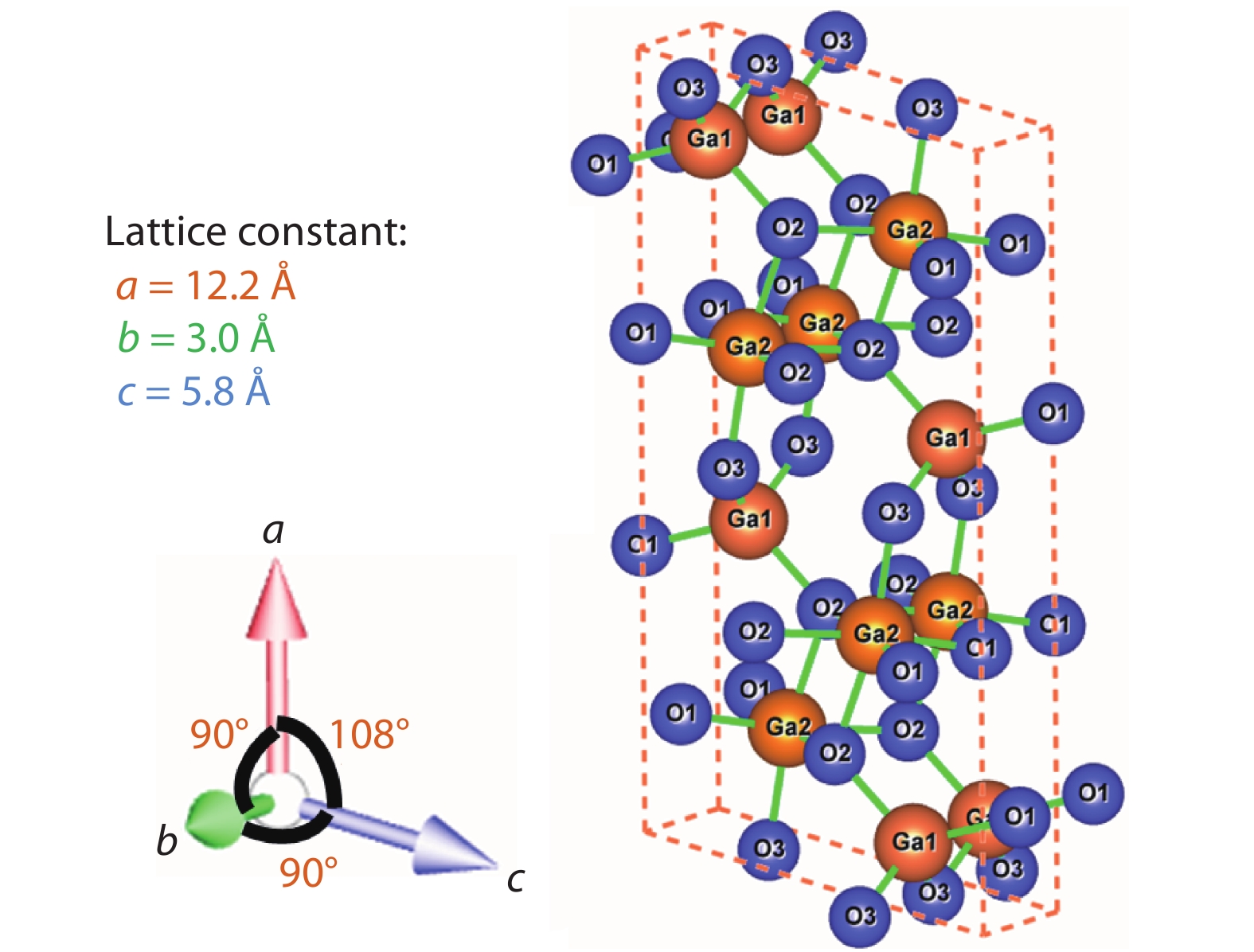
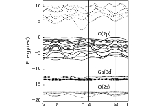
There are 5 polymorphs of β-Ga2O3, namely α, β, γ, δ, and ε[1015]. Among which, the monoclinic (β-) phase of β-Ga2O3 denotes the most stable one until its melting point, while other polymorphs are metastable and will convert into β phase at an elevated temperature (T) above 750–900 °C. The crystal structure and lattice parameters of β-Ga2O3 are shown in Fig. 1, with lattice constant a = 12.2 Å, b = 3.0 Å and c = 5.8 Å, respectively. The unit cell possesses two crystallographically inequivalent Ga positions, one with tetrahedral geometry Ga (I) and one with octahedral geometry Ga (II). The oxygen ions are arranged in ‘distorted cubic’ array. Oxygen atoms have three crystallographically different positions and are denoted as O(I), O(II) and O(III), respectively. Two oxygen atoms are coordinated trigonally and one is coordinated tetrahedrally. The different position of Ga and O atoms leads to an anisotropic optical, electrical and physical properties, for example its different thermal conductivity at (-201), (100), (010) and (100) planes. The upper valence and lower conduction band structure of β-Ga2O3, calculated from density functional theory (DTF) is shown in Fig. 2, as reported by He et al.[13]. It is generally accepted that the bandgap from DFT is underestimated due to the ground state theory. More accurate bandgap value of β-Ga2O3 is extracted to be around 4.8 eV from hybrid DFT, which is in agreement with absorption and resolved photoemission experiment[16, 17]. The electron effective mass is calculated to be around 0.3mo, where mo is the free electron mass. However, the flatness of valence band shows the large effective mass of holes, indicating an extremely low hole mobility even the p-type doping can be resolved. In addition to the challenges of the p-type doping and low hole mobility issues, the extremely low thermal conductivity of 10–25 W/(m·K) both from theoretical calculation and experiment turns out to be the most detrimental property of using β-Ga2O3 native substrate and potential solutions will be described in the future section.

Figure  1.  (Color online) Atomic unit cell of β-Ga2O3 with lattice constant and angle marked.
Figure  2.  Band structure of β-Ga2O3 with Fermi energy aligned to zero. Reprint from Appl Phys Lett, 88, 261904 (2006). Copyright 2006 American Institute of Physics.

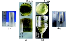
The success achieving of large diameter single crystalline and low defect density β-Ga2O3 native substrates is the main stimulation of devoting tremendous efforts to realize the application of β-Ga2O3 based materials and devices. Particularly, the development of melt-grown method offers the great promise of accomplishing low cost commercial substrates, which is advantageous over the growth techniques of SiC and bulk GaN. Standard growth techniques of β-Ga2O3 including Czochralski method (CZ)[1820], edge-defined film fed (EFG)[21], floating-zone (FZ)[2224] and vertical Bridgman (VB)[2527] growth methods. Tomm et al. first studied the CZ growth of the β-Ga2O3 single crystals and later Galazka et al carried out a comprehensive study on the same method[28, 29]. It is reported that a diameter of 2 inches cylindrical β-Ga2O3 single crystal have been demonstrated with this CZ method. It is generally accepted that the EFG is the most promising growth method for β-Ga2O3, combing the capability of achieving large size and high quality for future high-volume production, which is also a standard method for sapphire substrate. Growth rate as high as 15 mm/h and large size of 4 inches have been accomplished even at this premature stage, as shown in Fig. 3[30]. FZ method is always used as a route to synthesis β-Ga2O3 rod for basic research purpose with typical growth rate of 6 mm/h and diameter of 10 mm. VB methods provide another useful alternative methodology to achieve β-Ga2O3 single crystals by providing the advantage of easy release of the crystals after growth. The single crystal with diameter of 25 mm is obtained through this method, as shown in Fig. 4[31]. It should be noted that the unintentional incorporation of the Si and Ir atoms from the β-Ga2O3 seed and crucible leads to the unintentionally doped (UID) n-type conducting in the material so that deep acceptors like Mg and Fe are commonly used to compensate those n-type dopants to achieve the semi-insulating property.

Figure  3.  Photograph of 4-inch-diameter β-Ga2O3 wafer. Reprinted from Higashiwaki et al., J Phy D, 50 (2017). Copyright 2017 IOP Publishing[30].
Figure  4.  (Color online) β-Ga2O3 crystals grown by the VB method in either (a) a full-diameter crucible (a’), and (b) or in a conical crucible (b’). Reprinted from Hoshikawa et al., J Cryst Growth 447, 36 (2016). Copyright 2016 Elsevier[31].

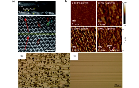
Developing high quality β-Ga2O3 thin film epitaxial growth is of equal importance when compared to the β-Ga2O3 substrate, since β-Ga2O3 thin film always serve as the channel layer for power devices such as diodes and MOSFETs. Accurate control of the dopants and minimization of defects and imperfections are always two challenges for thin film epitaxial growth. Homoepitaxial growth of high quality β-Ga2O3 thin films on its native substrates can be carried out by the following major ways: metalorganic chemical vapor deposition (MOCVD)[3234], molecular beam epitaxy (MBE)[3538], halide vapor phase epitaxy (HVPE)[3942], mist-CVD and some other CVD techniques[4349]. MOCVD and MBE are two of the most popular epitaxial growth tools, which are widely used in GaAs and GaN epitaxial growth. Baldini et al. reported on growing Sn-doped homoepitaxial layer on (100) substrate with MOCVD[50]. TEGA, molecular oxygen (O2) and TESn were used as Ga, O and Sn precursors, respectively. The epi-layer has a RMS surface roughness of 0.6 nm and the main defects in the layers were stacking faults and twin lamella. Gogova et al. reported on achieving single-phase, smooth β-Ga2O3 layers doped with Si, with a dislocation density not exceeding those of the melt grown substrate. HRTEM image of grown thin film is shown in Fig. 5(a)[33]. Okumura et al. reported on using plasma-assisted MBE to grow the (010) β-Ga2O3 under Ga-rich conditions at growth temperatures above 650 °C with growth rate about 2.2 nm/min. Slightly Ga-rich conditions between 650 and 750 °C are optimal for a smooth surface with an RMS surface roughness of 0.1 nm at a high growth rate. Surface roughness at various growth temperature is shown in Fig. 5(b)[37]. HVPE is one of the most cost effective methodologies in terms of deposition rate, epi-layer quality and inexpensive facility. However, it generally ends up with a rough surface, which requires a post chemical mechanical polishing process to smooth. Murakami et al. reported on using GaCl and O2 precursors for the HVPE of β-Ga2O3 thin film on (001) β-Ga2O3 substrate with a relative smooth surface morphology and low net carrier doping concentration of 1013 cm−3 at a limited growth rate of 5 μm/h and temperature of 1000 °C. The microscopy images of β-Ga2O3 surfaces after HVPE growth on (001) β-Ga2O3 substrates for 1 h at (c) 800 and (d) 1000 °C[41] are shown in Fig. 5. Mist CVD is another inexpensive approach to grow different polymorphs of Ga2O3, like α-, β-, γ-phases at a relatively low growth temperature of 500–630 °C, while the solution is atomized via ultrasonication at a frequency of 2.4 MHz. Other phases can be transformed into β-phase after a high temperature annealing.

Figure  5.  (Color online) (a) HRTEM image of an undoped homoepitaxial β-Ga2O3 layer from MOVPE method. (b) Surface morphologies of 60-nm-thick β-Ga2O3 (010) layers grown on Sn-doped β-Ga2O3 (010) substrates at a growth rate of 1 nm/min under slightly Ga-rich conditions at the growth temperatures of 500, 700, 800, and 900 °C, respectively. NDIC microscopy images of β-Ga2O3 surfaces after HVPE growth on (001) β-Ga2O3 substrates for 1 h at (c) 800 and (d) 1000 °C. Reprinted from Refs. [33, 37, 41].

As always emphasized by the β-Ga2O3 community, β-Ga2O3 holds promise for future power electronics due to its ultra-wide bandgap, high breakdown field and decent electron mobility induced high BFOM. Table 1 lists the comparisons of some major semiconductors as the channel materials for power devices. Some key FOMs used for representing how ideal of this material can be utilized for power electronics, such as Baliga, Johnson and Keys are also included. Baliga, Baliga high frequency, Johnson and Keyes FOMs are used to evaluate the power devices in terms of power handling capability and conduction loss, the measure of switching losses, the measure of suitability of a semiconductor material for high frequency power transistor applications and requirements, and the thermal dissipation capability for power density and speed, respectively. As shown in this Table 1, all other FOMs of β-Ga2O3 are significantly higher than that of SiC and GaN except Keyes FOM due to its obvious shortage of extremely-low thermal conductivity. Nevertheless, we should put all our endeavors to explore and demonstrate all its potentials and then push the device performance to its limit. Diodes and FETs are the most basic but most important elements of power electronics, which deserve thorough investigation. In this section, the most recent progresses of both diodes and FETs are comprehensively reviewed and solution to its low thermal conductivity issue is proposed.

Table  1.  Properties of β-Ga2O3 relative to some other major semiconductors used for power electronics applications, considering their different kinds of FOM.
Material Parameter Si GaAs 4H-SiC GaN Diamond β-Ga2O3
Bandgap Eg (eV) 1.14 1.43 3.25 3.4 5.5 4.8
Dielectric constant ε 12 13 10 9 5.5 11
Breakdown field EC (MV/cm) 0.3 0.4 2.5 3.3 10 8
Carrier mobility μ (cm2/(V·s)) 1450 8400 1000 1200 2000 300
Saturation velocity νsat (107 cm/s) 1 1.2 2 2.5 1 2
Thermal conductivity κ (W/mK) 150 50 370 250 2000 10–30
FOM relative to Si
Baliga FOM = εμEc3 1 14.7 317 846 24 660 3200
Johnson FOM = Ec2νsat2/4π2 1 1.8 278 1089 1110 2844
Baliga High Frequency FOM = μEc2 1 10 46 100 1500 142
Keyes FOM = κ[(sat)(4πε)]1/2 1 0.3 3.6 1.8 41.5 0.2
DownLoad: CSV  | Show Table

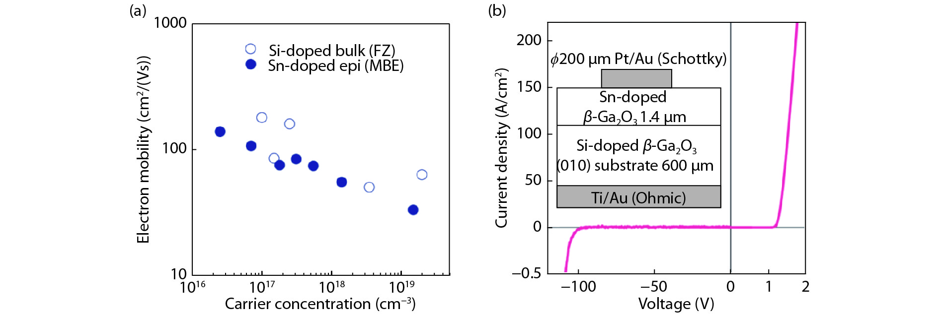
Schottky Barrier Diodes (SBDs) with low turn on voltage (Von), high forward current density and fast switching speed properties are ideal candidate for low switching/conduction losses and high frequency operations, which are indispensible components in power electronic circuits such as converters and inverters for power supplies and power factor corrections[51]. Sasaki et al. developed the first β-Ga2O3 SBD on its (010) native substrate with a 1.4 μm thick ozone MBE homoepitaxial grown drift layer and a breakdown voltage (BV) of more than 100 V is achieved[52]. The electron mobility of this Sn-doped thin film is reported to be as high as 100–150 cm2/(V·s) at a doping concentration range of 1016–1017 cm−3. The mobility versus doping concentration and I–V characteristics are included in Fig. 6.

Figure  6.  (Color online) (a) Electron mobility as a function of carrier concentration. (b) I–V characteristics of Pt/β-Ga2O3 Schottky barrier diodes. The inset shows the schematic structure of the β-Ga2O3 SBD. Reprinted from Sasaki et al., Appl Phys Express, 5, 035502 (2012)[52]. Copyright of 2012 Japanese Society of Applied Physics.

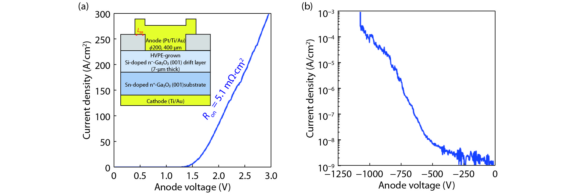
Following the 1st β-Ga2O3 SBD, many research groups have demonstrated high performance SBDs with BV around or exceeding 1 kV with or without field-plate or edge termination techniques. Konishi et al. reported on the 1st achieving of the BV more than 1 kV with a field-plate structure and a 7-μm thick HVPE grown β-Ga2O3 drift layer[53]. Diodes were fabricated by depositing full area back Ohmic contacts of Ti/Au (20 nm/230 nm) by E-beam evaporation, while the Schottky contacts were patterned by lift-off of E-beam deposited Schottky contacts Pt/Ti/Au (15 nm/5 nm/500 nm) on the epitaxial layers with a field plate length of 20 μm. The net donor concentration of this epitaxial layer is calculated to be 1.6 × 1016 cm−3 from C–V measurement. To achieve a high BV, a low density channel or drift layer is needed so as to flatten the electric field from the anode to cathode based on the Poisson Equation. The device has a specific on-resistance of 5.1 mΩ·cm2, yielding a power FOM of 227 MW/cm2, combined with the BV of 1076 V. The peak E at anode edge is simulated to be 5.1 MV/cm, which is much higher than the EC of GaN and SiC. Fig. 7 shows the details of the device schematic, forward and reverse J–V characteristics.

Figure  7.  (Color online) (a) Forward and (b) reverse J–V characteristics of β-Ga2O3 FP-SBD at room temperature. Inset shows the cross-section device schematic of the vertical SBD. Reprinted from Appl Phys Lett, 110, 103506 (2017). Copyright 2017 American Institute of Physics[53].

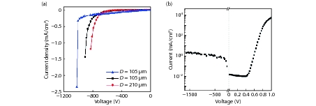
Yang et al. also demonstrated 1 kV-class vertical β-Ga2O3 SBD without field-plate structure with a 10-μm thick β-Ga2O3 drift layer and Ni/Au as the anode[54]. The native substrate possesses a pit dislocation of 103 cm−2 and the epitaxial layer has a net doping concentration of 2 × 1016 cm−3. It is found that the BV has a strong dependence on the anode diameter and the BV is around 1 KV and 800 V at an anode diameter of 105 and 205 μm, respectively, as shown in Fig. 8(a). The diode is also reported to achieve a high power FOM of 150 MW/cm2 with a Ron,sp of 6 mΩ·cm2. By further shrinking the anode diameter to 25 μm, the BV is further increased to be 1.6 kV at a decent power FOM of 100 MW/cm2, as shown in Fig. 8(b)[55]. This anode diameter dependent BV is most likely related with defects in the epitaxial layer. With larger anode area, higher quantities of defects are expected underneath the anode so that once a point defect is damaged under the high E condition the whole diode is destroyed, resulting in a reduced BV. Through growth optimization, the carrier concentration in the epitaxial layer can be further reduced to 2 × 1015 cm−3. Combined with a 20-μm thick drift layer, the BV can be enhanced to 2300 V. Meanwhile, a high current of 2 A can be also achieved by enlarging the anode area to 0.2 cm2[56].

Figure  8.  (Color online) (a) Reverse I–V characteristics of 3 diodes with two different diameters, showing a diameter dependence of the BV, and (b) forward and reverse I–V characteristics from a 20 μm diameter diode. Reprinted from Appl Phys Lett, 110, 192101 (2017) and IEEE Electron Device Lett. Copyrights 2017 American Institute of Physics and 2017 IEEE[54, 55].

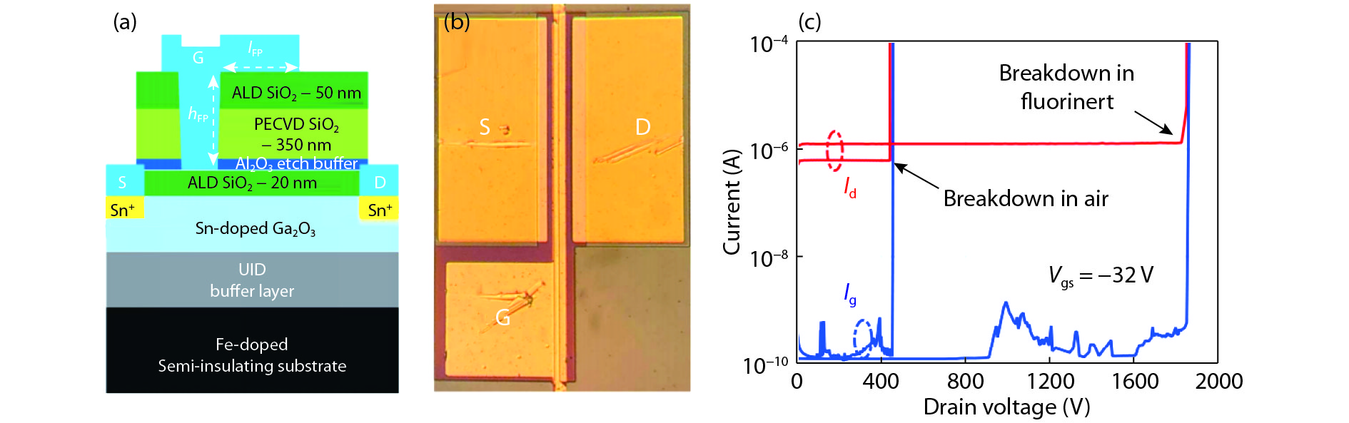
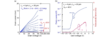
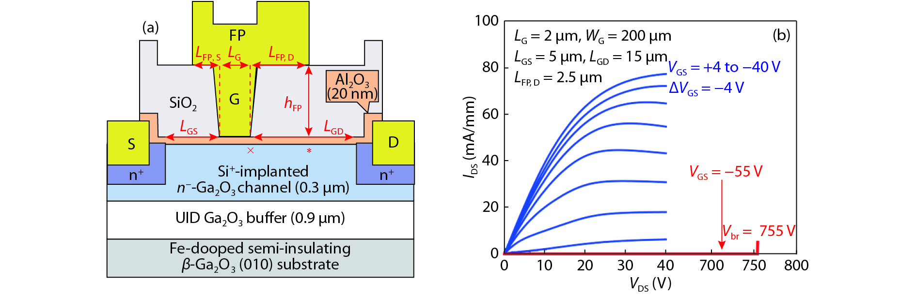
The first metal-semiconductor-FET (MESFET) was demonstrated by Higashiwaki et al. with a Sn-doped β-Ga2O3 epitaxial channel on a semi-insulating (010) β-Ga2O3 substrate[57]. This circular MESFET is with a gate length (LG) of 4 μm and source-drain (LSD) of 20 μm demonstrates a BV of more than 250 V, drain current (ID) of 15 mA and on/off ratio around 104. Output and transfer characteristics are plotted in Fig. 9. Following the MESFET, metal-oxide-semiconductor FETs (MOSFETs) start to attract the power device community’s attention to resolve the shortcomings of the MESFET. The first lateral depletion-mode (D-mode) β-Ga2O3 MOSFET power device with BV more than 600 V was reported by Wong et al.[58]. The device structure is shown as Fig. 10(a) with a MBE grown and Si-doped channel with doping concentration of 3 × 1017 cm−3, a heavily doped source and drain contacts and a FP length of 2.5 μm. A maximum ID of 80 mA/mm, peak gm of 3.5 mS/mm and high on/off ratio of more than 109 are achieved simultaneously. Pulsed IDVDS shows no current collapse phenomenon, verifying the great promise of β-Ga2O3 MOSFET as a candidate for power device application. Recently, Zeng et al. has pushed the BV to be 1850 V by adopting a FP structure and a 400-nm thick composite field plate oxide at a LGD = 20 μm[59]. It is believed that the introduction of another 50 nm of ALD SiO2 is helpful in improving the BV, rather than a simply plasma-enhanced CVD (PECVD) SiO2 layer underneath the gate FP electrode, where the premature breakdown happens and also a high-quality ALD SiO2 is available to sustain a higher EC. The device structure and breakdown characteristics are described in Fig. 11.

Figure  9.  (Color online) (a) DC output characteristics of β-Ga2O3 MESFET and (b) transfer characteristics of the same MESFET at VDS = 40 V. Reprinted from Appl Phys Lett, 100, 013504 (2012). Copyrights 2012 American Institute of Physics[57].
Figure  10.  (Color online) (a) Schematic cross section of a β-Ga2O3 MOSFET with a gate-connected FP structure and (b) Output characteristics of the MOSFET with maximum ID of 78 mA/mm and BV of 750 V. Reprinted from IEEE Electron Device Lett, 37, 2 (2016). Copyright of 2016 IEEE[58].
Figure  11.  (Color online) (a) Cross-section view and (b) optical image of the fabricated field-plated Ga2O3 MOSFET with SOG S/D doping. (c) Three-terminal breakdown measurement of the field-plated Ga2O3 MOSFET and a record-high BV of 1850 V is demonstrated. Reprinted from IEEE Electron Device Lett, 39, 9 (2018). Copyright of 2018 IEEE[59].

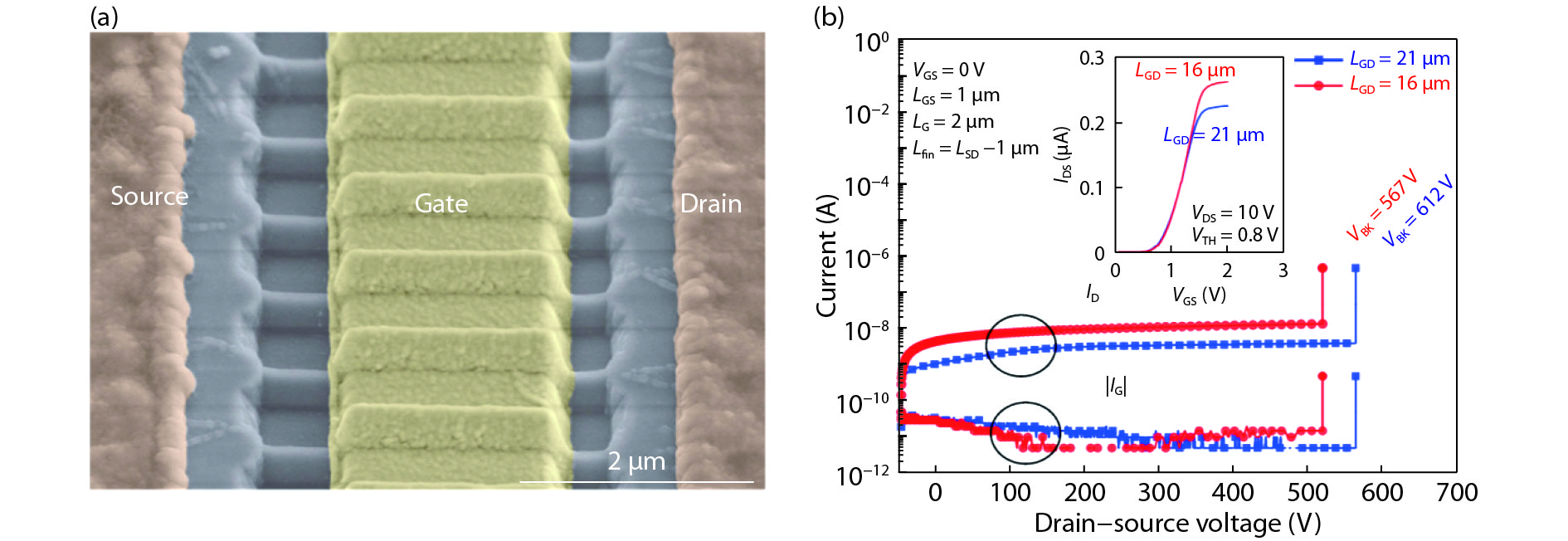
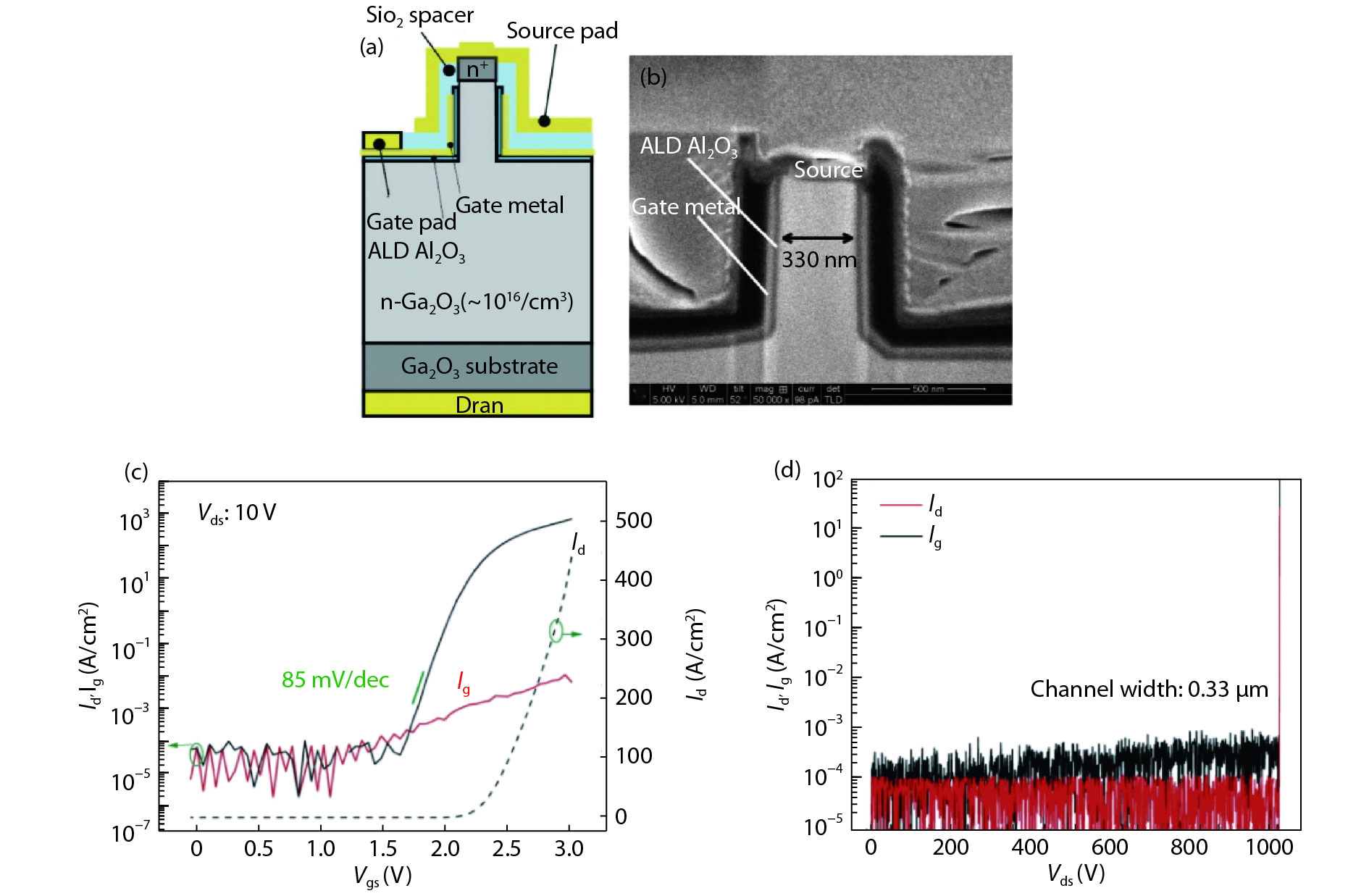
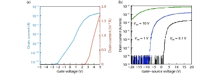
Zeng et al. reported on achieving the first E-mode β-Ga2O3 MOSFET by adopting a high work function Au gate electrode and low doping (6 × 1015 cm−3) MBE β-Ga2O3 channel, so that E-mode operation with VT of 3 V and BV of 400 V are demonstrated[60]. Later, Tadjer et al. fabricated a (001) β-Ga2O3 MOSFET with VT = 2.9 V and HfO2 as the gate dielectric[5]. Figs. 12(a) and 12(b) are the IDVGS characteristics of Zeng’s and Tadjer’s E-mode MOSFET. Chabak et al. demonstrated the E-mode β-Ga2O3 MOSFET via incorporating a fin-array structure with triangular fin-width of 300 nm and fin-height of 200 nm, such that the high work function Ni gate electrode can deplete the β-Ga2O3 channel from two side walls with VT around 1 V[4]. On/OFF ratio greater than 105 and a three-terminal BV of more than 600 V are achieved at a 21-μm gate-drain spacing, as shown in Fig. 13. Hu et al. has adopted a similar Fin-structure to achieve an E-mode operation on a vertical MOSFET[61]. A 10-μm thick HVPE β-Ga2O3 layer on (001) substrate with low charge doping concentration of 2 × 1016 cm−3 is used as the starting wafer. By shrinking the fin-width to 330 nm or even smaller, the VT is extracted to be 1.2–2.2 V. A current on/off ratio of 108, Ron,sp of 13–18 mΩ·cm2, BV up to 1057 V and output current of more than 200 A/cm2 are demonstrated. Figs. 14(a)14(d) depict the device structure of the vertical E-mode β-Ga2O3 MOSFET, on-state IDVGS and three-terminal OFF-state breakdown measurement results, respectively.

Figure  12.  (Color online) IDVGS characteristics of (a) Zeng’s and (b) Tadjer’s E-mode MOSFET. Reprinted from IEEE Device Research Conf and ECS J, Solid State Sci, Technol, 39, 9 (2018). Copyright of 2016 IEEE[60] and 2016 ECS[5].
Figure  13.  (Color online) (a) Tilted false-colored SEM image of a fabricated E-mode β-Ga2O3 Fin-MOSFET and (b) The breakdown characteristics of β-Ga2O3 Fin-MOSFET with LG = 2 μm and LGD = 16, 21 μm at VGS = 0 V. The inset shows the transfer characteristics of the same device indicating a VTH = 0.8 V. Reprinted from Appl Phys Lett, 109, 213501 (2016). Copyrights 2016 American Institute of Physics[4].
Figure  14.  (Color online) (a) Schematic cross-section and (b) SEM image of a vertical E-mode β-Ga2O3 Fin-MOSFET, (c) transfer characteristics of the device with a VTH = 2.2 V, on/off ratio of 108, and on-current of 400 A/cm2. (d) The breakdown characteristics of β-Ga2O3 Fin-MOSFET with channel width of 330 nm. Reprinted from IEEE Electron Device Lett, 39, 869, 2018. Copyright of 2018 IEEE[61].

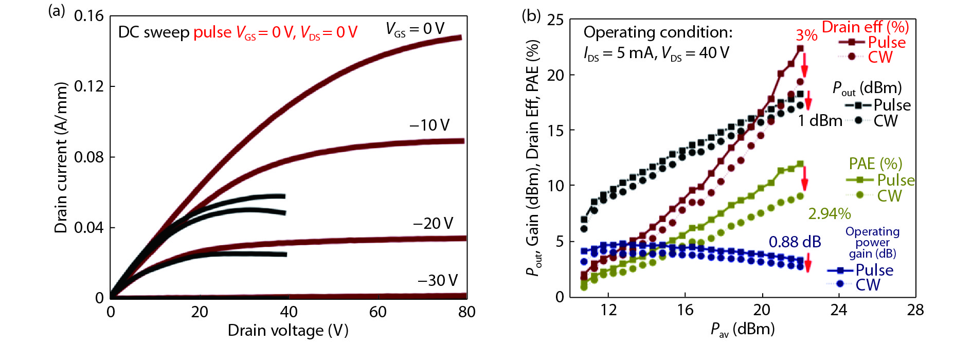
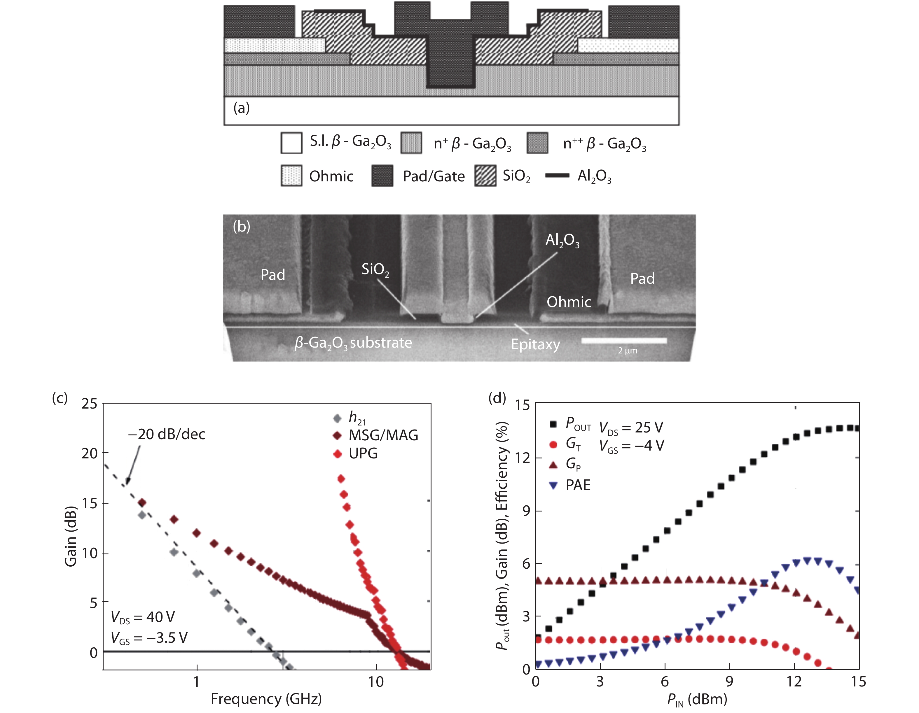
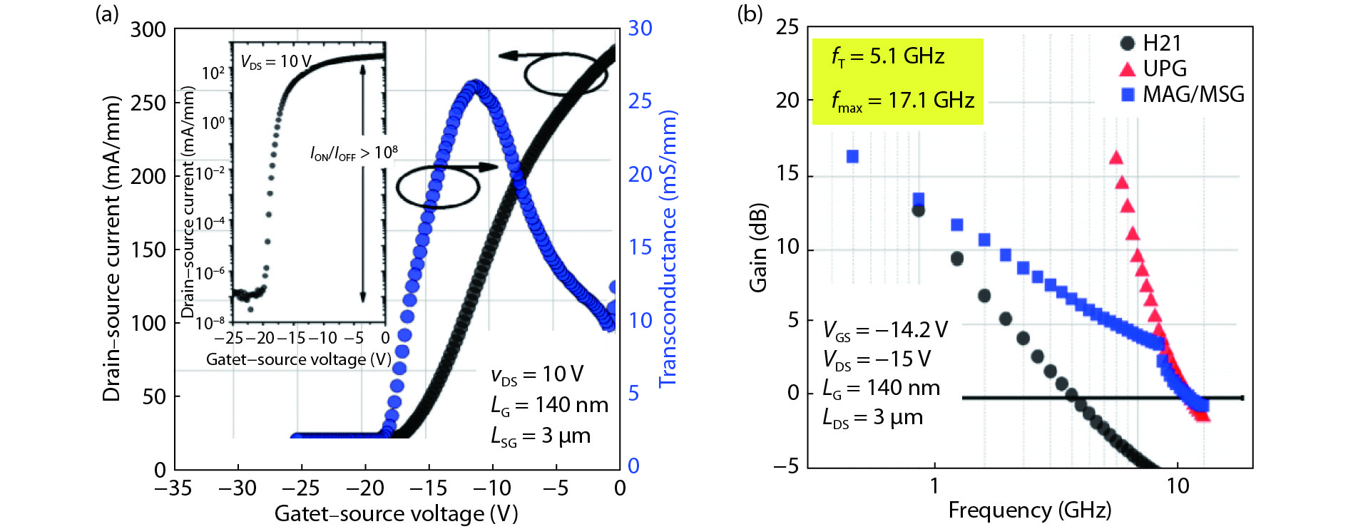
Green et al. reported on demonstrating the first β-Ga2O3 RF transistor on a Si-doped MOCVD β-Ga2O3 channel with doping concentration of 1018 cm−3 and a (100) substrate[62]. By recessing the β-Ga2O3 epi-channel, peak transconductance of 21 mS/mm and extrinsic cut-off frequency (fT) and maximum oscillation frequency (fmax) of 3.3 GHz and 12.9 GHz are achieved. Meanwhile, CW class-A power amplifier demonstrate a output power density (Pout), power gain, and power-added efficiency (PAE) of 0.23 W/mm, 5.1 dB and 6.3%, respectively at the frequency of 800 MHz. Device structure, small signal and large signal performances are described in Fig. 15. Singh et al. carried out the study on the pulsed large signal RF performance of field-plated β-Ga2O3 MOSFET[63]. It is revealed that reduced self-heating when pulse resulted in a PAE of 12%, drain efficiency of 22.4%, Pout of 0.13 W/mm and a maximum gain up to 4.8 dB at 1 GHz for a device with Lg = 2 μm. Self-heating effect at high VDS and IDS caused by the low thermal conductivity is the main factor limiting the device performances, while the trapping effect has the minimal impact on the performance degradation. Pulsed IDVDS measurement and large signal load pull measurement results are shown in Fig. 16 and the comparison between CW and pulsed results are shown in Table 2, indicating the self-heating effect is the primary detrimental factor of degrading device performance. Chabak et al. reported on achieving high performance β-Ga2O3 RF transistor by utilizing a higher doped but thinner Si doped MOVPE (100) channel with sub-micron T-shape gate[64]. A record-high fT/fmax of 5/17 GHz at VDS = 15 V and VGS = −14.2 V is achieved, along with a peak gm of 25 mS/mm. DC and RF results are shown in Fig. 17.

Figure  15.  (Color online) (a) A device cross section schematic is shown for the β-Ga2O3 MOSFET under test. (b) A focused ion beam (FIB) cross sectional image of the device. (c) Extrinsic small signal RF gain performance recorded at VGS = −3.5 V (peak gm) and VDS = 40 V (d) 800 MHz Class-A power sweep of a 2 × 50 μm β-Ga2O3 gate recessed MOSFET. Reprinted from IEEE Electron Device Lett, 38, 790, 2017. Copyright of 2017 IEEE[62].
Figure  16.  (Color online) (a) DC output characteristics and pulsed IV from a quiescent bias of VGS = VDS = 0 V up to VDS = 80 V with 1 μs pulse length and 1 ms period (b) Pulsed and CW large signal measurements at 1 GHz with input available power sweep up to 22 dBm, measured at VDS = 40 V with IDS = 5 mA. Reprinted from IEEE Electron Device Lett, 39, 1572, 2018. Copyright of 2018 IEEE[63].
Table  2.  Comparison of CW and pulse large signal measurements performed at two different operating power levels of 0.4 and 0.8 W/mm. larger differences in performance between cw and pulsed modes can been seen with increasing operating power. Reprinted from IEEE Electron Device Lett, 39, 1572, 2018. Copyright of 2018 IEEE.
Parameter Operating condition 0.4 W/mm 25 °C
(IDS = 5 mA, Vds = 40 V)
Operating condition 0.8 W/mm 25 °C
(IDS = 10 mA, VDS = 40 V)
CW Pulse CW Pulse
Pout (dBm) 17.42 18.28 17.63 19.52
Pout (W/mm) 0.11 0.13 0.11 0.17
Drain Eff (%) 19.56 22.40 13.83 17.04
PAE (%) 9.09 12.01 3.23 6.85
Max gain (dB) 4.17 4.81 2.08 3.68
Channel temperature (°C) 58 28 97 36
DownLoad: CSV  | Show Table
Figure  17.  (Color online) Transfer characteristics of the thin-channel BGO MOSFET with T-gate. The GM reaches 25 mS/mm with current density over 275 mA/mm, and the inset shows a good ION/IOFF ratio greater than 108. (b) Small signal gain at VDS = 15 V of the thin-channel BGO MOSFET with ft/fmax = 5.1/17.1 GHz. Reprinted from IEEE IMWS-AMP, 2018. Copyright of 2018 IEEE[64].

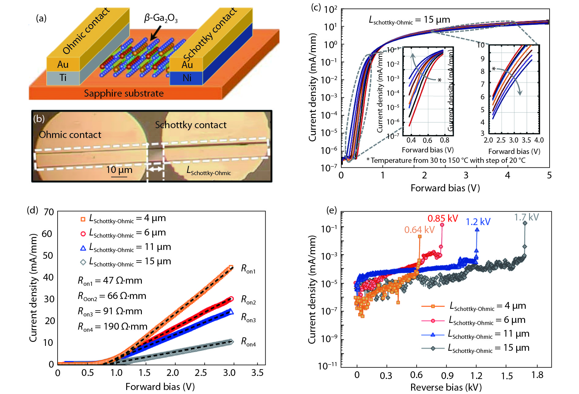
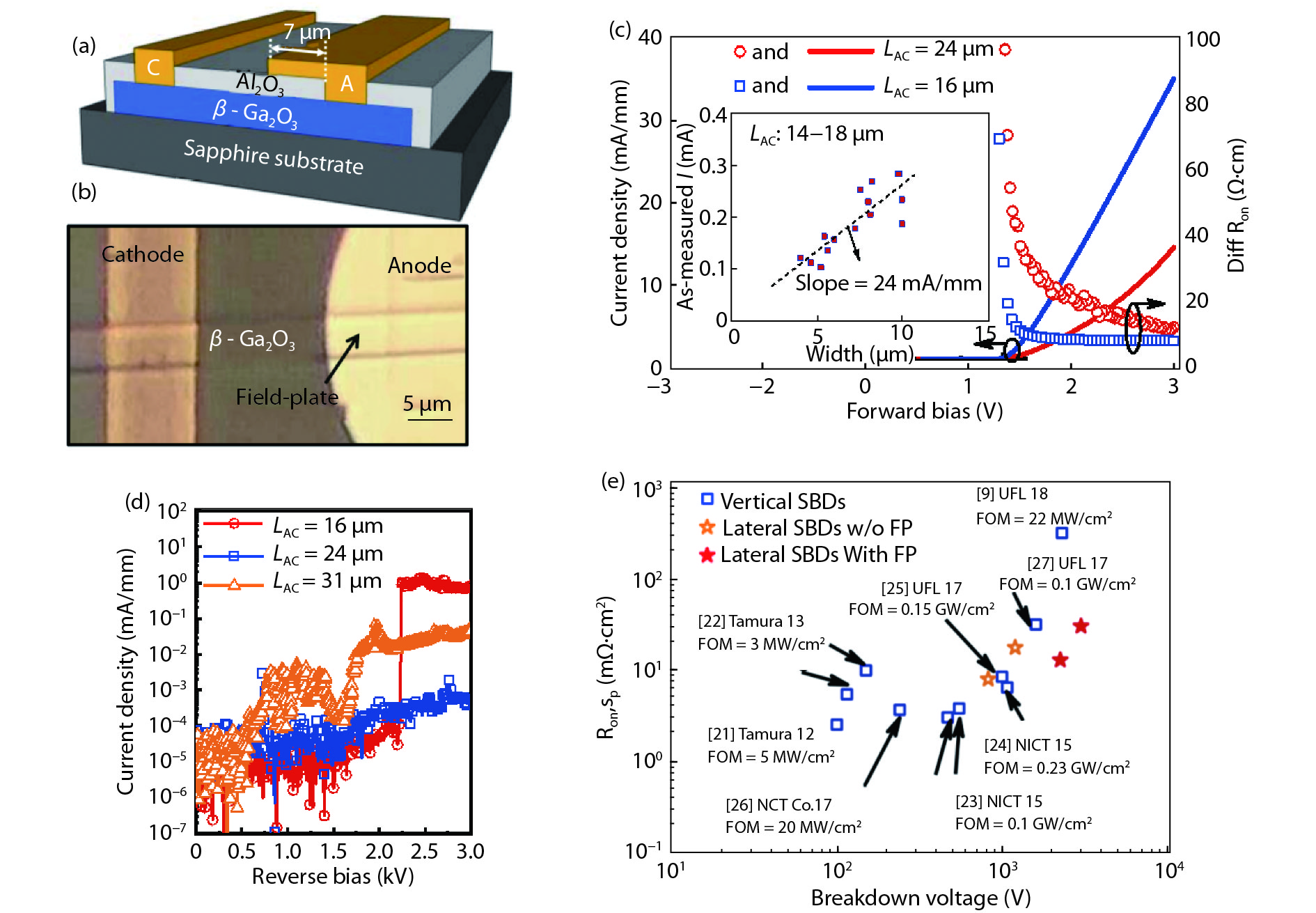
β-Ga2O3 crystal possesses an unique property that its (100) surface has a large lattice constant of 12.23 Å along [100] direction, which allows a facile cleavage into thin belts or nano-membranes[65]. Hence, by transferring β-Ga2O3 nano-membrane from its bulk substrate to a wider bandgap and higher thermal conductivity substrate can minimize low-thermal conductivity of β-Ga2O3 bulk substrate induced severe self-heating effect while maintaining its high breakdown characteristics. Importantly as a research route, it provides an effective methodology to investigate fundamental material property of β-Ga2O3 and fully explore device potentials without using many β-Ga2O3 epitaxy wafers. Hu et al. reported on the first high performance lateral β-Ga2O3 SBD on sapphire substrate by transferring high quality β-Ga2O3 nano-membrane channel from its low defect density bulk substrate[66]. Annealed Ti/Au (60/120 nm) is used as the cathode while Ni/Au (60/120 nm) is used as the anode metal and the β-Ga2O3 nano-membrane is with thickness around 400 nm. The SBDs have an on-current on/off ratio of 107–108 with turn-on voltage (Von) of 1 V determined by the linear extrapolation of the forward I–V. The Ron, sp of each SBD is determined to be Ron = 3.29, 5.94, 12.7, and 34.2 mΩ·cm2 for LSchottky-Ohmic = 4, 6, 11, and 15 μm, respectively. The off-state BV is measured to be 0.64 kV, 0.85 kV, 1.2 kV and 1.7 kV, yielding a power FOM of 0.124, 0.121, 0.113, and 0.09 GW/cm2 for LSchottky-Ohmic = 4, 6, 11, and 15 μm, respectively, by considering the FOM = BV2/Ron, sp. Device structure, forward I–V and reverse breakdown characteristics are shown in Fig. 18. Following the first lateral β-Ga2O3 SBD, Hu et al. also developed a field-plated lateral β-Ga2O3 SBD with record-high reverse blocking voltage of more than 3 kV and high DC power FOM of 500 MW/cm2[51]. In this study, an even thicker (650 nm) β-Ga2O3 nano-membrane channel is used to improve the on-current and hence reducing the Ron,sp and the field plate structure is used to mitigate the E crowding effect at the anode edge. The record-high BV of more than 3 kV is demonstrated on a SBD with LSchottky-Ohmic = 24 μm with low Ron,sp of 24.3 mΩ·cm2. In addition to the high BV of more than 3 kV, a record high power FOM of 0.5 GW/cm2 is also achieved on the SBD with LSchottky-Ohmic = 16 μm and BV = 2.25 kV. The device structure, reverse characteristics and benchmark comparisons between lateral and vertical SBDs are shown in Fig. 19.

Figure  18.  (Color online) (a) Schematic-view and (b) top-view microscopy image of a fabricated lateral β-Ga2O3 SBD on sapphire substrate. (c) Log-scale forward characteristics of β-Ga2O3 SBD with LSchottky-Ohmic = 15 μm at the temperature range from 30 to 150 °C with 20 °C as a step. (d) Linear-scale forward I–V characteristics of β-Ga2O3 SBDs with various LSchottky−Ohmic. (e) Reverse I–V characteristics of lateral β-Ga2O3 SBDs with various LSchottky−Ohmic. Reprinted from IEEE JEDS 6, 815, 2018. Copyright of 2018 IEEE[66].
Figure  19.  (Color online) (a) Tilted 3-D schematic-view and (b) top-view microscopy image of a fabricated lateral field-plated β-Ga2O3 SBD on Sapphire substrate. (c) Forward I–V and differential RonV characteristics in linear scale. The inset shows as-measured current dependence on the width of the SBD at a similar LAC of 14–18 μm. (d) Reverse I–V characteristics of lateral SBDs with field plate structure and various LAC. (e) DC RON,SP versus BV of some both lateral and vertical β-Ga2O3 SBDs. Reprinted from IEEE Electron Device Lett, 39, 1564, 2018. Copyright of 2018 IEEE[51].

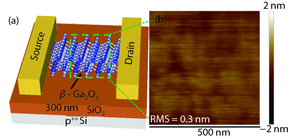
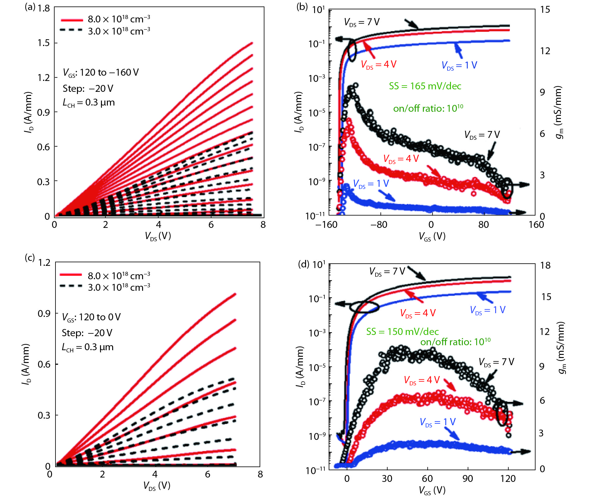
Zhou et al. reported on achieving record-high on-current with a back-gated FETs based on β-Ga2O3 nano-membrane channels[67, 68]. Figs. 20(a) and 20(b) are the schematic of a GOOI FET and atomic force microscopy (AFM) image of a β-Ga2O3 surface after cleavage, which shows atomically flat and uniform within the whole nano-membrane. Device fabrication commenced with 6 mm by 6 mm (-201) β-Ga2O3 bulk substrate with Sn doping concentration of 3 × 1018 cm−3 and 8 × 1018 cm−3. Various β-Ga2O3 nano-membranes with thickness from 50 to 150 nm, confirmed by the AFM measurements, were chosen for the device fabrication. Fig. 21(a) presents the D-mode DC output characteristics (IDVDS). Devices have a LCH of 0.3 μm, channel width (W) of 0.15 μm and channel thickness (t) of 70 nm for 8.0 × 1018 cm−3, and W = 0.6 μm and t = 100 nm for 3.0 × 1018 cm−3 device, respectively. A record high maximum ID (IDMAX) of 1.5 A/mm is obtained, which is more than 2 times of lower doping channel. The device also has a much lower Ron of 5 Ω·mm compared with that of 11 Ω·mm with 3.0 × 1018 cm−3 doping concentration. Fig. 21(b) is the log-scale IDgmVGS transfer characteristics of the same D-mode GOOI FET with 8.0 × 1018 cm−3 doping concentration. This D-mode GOOI FET has a threshold voltage (VT) of −135 V, extracted from the log-scale IDVGS at VDS = 1 V and ID = 0.1 mA/mm. Figs. 21(c) and 21(d) depict the IDVDS output and IDgmVGS transfer characteristics of an E-mode GOOI FET with LCH = 0.3 μm, t = 55 nm and W = 0.17 μm for 8.0 × 1018 cm−3, and t = 75 nm and W = 0.45 μm for 3.0 × 1018 cm−3 device also shown in Fig. 21(c) as black dashed curves for comparison. A record high IDMAX = 1.0 A/mm for higher doping channel is obtained, which is more than 80% higher than lower doping channel. E-mode GOOI FET has a VT of 2 V determined from the IDVGS at VDS = 1 V and ID = 0.1 mA/mm. Further scaling the LCH shows no significant help in boosting the IDMAX, which is primarily limited by the high RC of low doping channel underneath the contact. The improved IDMAX of D/E-mode devices mainly originate from the higher doping concentration induced lower Rc rather than the simply LCH scaling. Finally, benefiting from its wide-bandgap and a low damage transfer process, both D/E-mode devices have achieved high on/off ratio of 1010 and low SS of 150–165 mV/dec for a 300 nm thick SiO2.

Figure  20.  (Color online) (a) Schematic view of a GOOI FET with a 300 nm SiO2 layer on Si substrate and (b) AFM image of the atomic flat β-Ga2O3 surface after cleavage. Reprinted from IEEE Electron Device Lett, 38, 103, 2017. Copyright of 2017 IEEE[68].
Figure  21.  (Color online) (a) and (c) are IDVDS output characteristics of D- and E-mode GOOI FETs with 3.0 × 10¹⁸ and 8.0 × 1018 cm−3 doping channel, respectively. (b) and (d) are IDgmVGS transfer characteristics of D-mode and E-mode GOOI FETs with 8.0 × 1018 cm−3 doping channel, respectively. Record high IDMAX of 1.5 and 1.0 A/mm are demonstrated for D/E mode devices. Both D and E-mode devices have high on/off ratio of 1010 and low SS of 150–165 mV/dec for 300 nm SiO2. Reprinted from Appl Phys Lett, 111, 092102, 2017. Copyright of 2017 AIP[67].

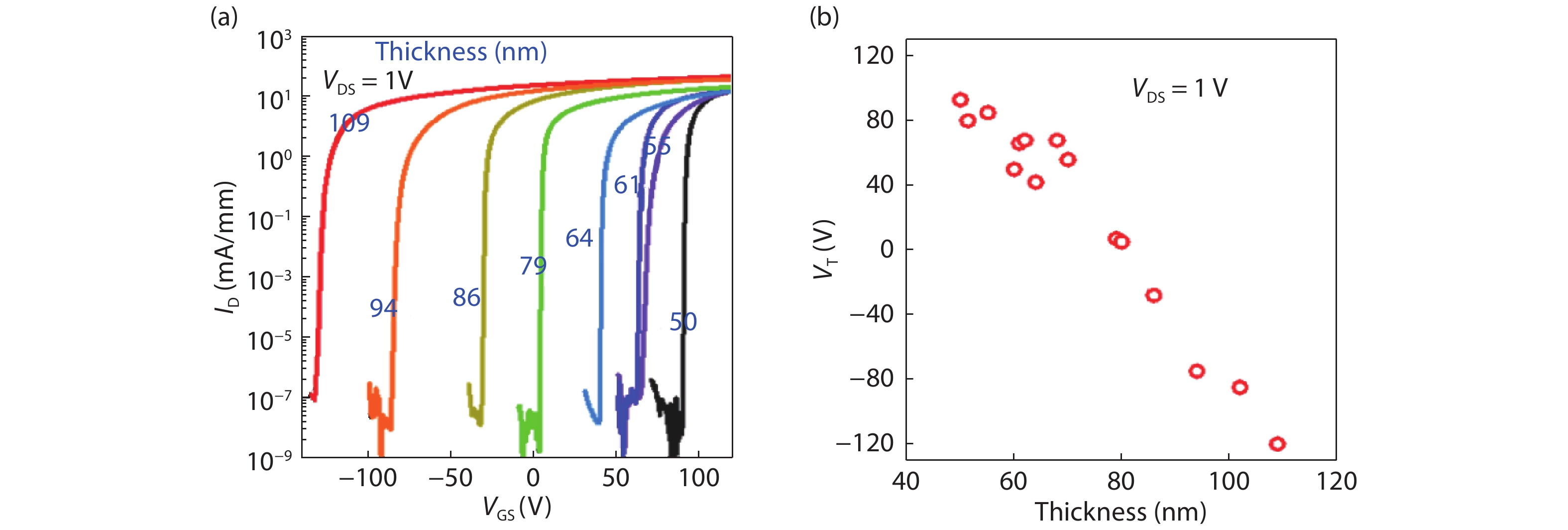
It is found that the VT shifts from negative values in D-mode to positive values in E-mode by shrinking β-Ga2O3 nano-membrane thickness. Fig. 22(a) describes the thickness dependent representative IDVGS characteristics. Obviously, the VT is shifted from negative to positive when the thickness is slowly reduced. Fig. 22(b) summarizes the extracted thickness dependent VT of 15 devices. Generally, they all follow the same trend as shown in Fig. 22(a). The determined thickness dependent VT may be valuable in the realization of high performance top gate E-mode GOOI FETs in the near future.

Figure  22.  (Color online) (a) Thickness dependent IDVGS plots of various GOOI FETs from D-mode of thicker β-Ga2O3 to E-mode of thinner β-Ga2O3. (b) Thickness dependent VT extracted at VDS = 1 V of 15 devices. Reprinted from IEEE Electron Device Lett, 38, 103, 2017. Copyright of 2017 IEEE[68].

The significant VT shift with respect to different β-Ga2O3 nano-membrane thickness is due to the surface depletion of the unpassivated device surface, which has tremendous dangling bonds and surface states on the device surface[69]. This is the reason why E-mode GOOI FETs can also be realized in high doping β-Ga2O3 nano-membrane. The surface depletion effect could be verified by using ALD to deposit 15 nm Al2O3 on top to passivate the top surface. As shown in Fig. 23(a), the VT is significantly shifted to the left for more than 70 V after an ALD passivation, verifying the existence of top and bottom surface depletion on unpassivated GOOI FET surfaces. Based on the surface depletion, each surface depleted charge density (ns) can be estimated by using the TCAD C–V simulation to match the measured and simulated VT from E-mode devices with VT near zero. The ns is determined and simulated to be 1.2 × 1013 cm−2 and 2.2 × 1013 cm−2 for 3.0 × 1018 cm−3 and 8.0 × 1013 cm−3 nano-membranes with thickness of 80 nm and 55 nm, respectively. Higher ns for higher doping β-Ga2O3 nano-membrane is most likely related to the higher surface states with more Sn+4 dopants. Therefore, the actual C–V curve and IDVGS curves are significantly shifted to the right compared with the ideal case without considering surface depletion. Fig. 23(b) shows the simulated C–V curve for E-mode GOOI FET and the VT from C–V simulation is in good agreement with the VT from IDVGS characterization. Figs. 23(c) and 23(d) are the simulated band diagram of the E-mode GOOI FET at VGS = 0 V with lower doping and higher doping channels by considering surface depletion effect. The top and bottom depletion regions pull up the conduction band of β-Ga2O3 with very few carriers left behind in the nano-membrane, so that E-mode GOOI FET can be formed.

Figure  23.  (Color online) (a) IDVGS comparison between GOOI FETs with and without ALD passivation for β-Ga2O3 nano-membrane with doping concentration of 3.0 × 1018 cm−3, (b) simulated C–V curve for E-mode GOOI FET at a β-Ga2O3 nano-membrane thickness of 80 nm and doping concentration of 3.0 × 1018 cm−3 after considering the top and bottom negative surface charge (ns = 1.2 × 1013 cm2) depletion effect. Band diagram and electron density distribution of E-mode GOOI FETs with surface negative charge depletion on (c) lower doping (ns = 1.2 × 1013 cm−2) and (d) high doping (ns = 2.2 × 1013 cm−2) β-Ga2O3 nano-membrane channels at VGS = 0 V. Reprinted from Appl Phys Lett, 111, 092102, 2017. Copyright of 2017 AIP[67].

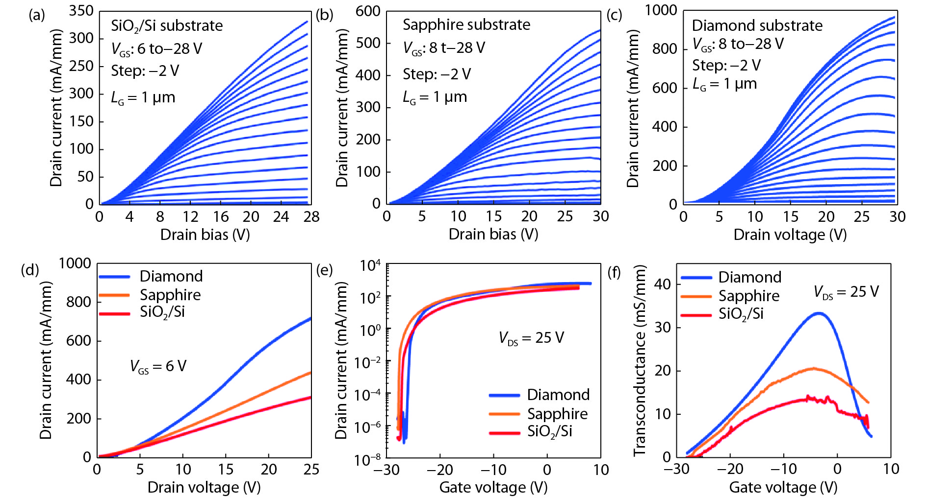
Self-heating effect induced temperature increase and non-uniform distribution of dissipated power have emerged as one of the most dominant concerns in the degradation of the ID, output power density (P), as well as the gate leakage current, device variability, and reliability[70]. This effect would become severe in high power device with a low thermal conductivity (κ) substrate such as β-Ga2O3, whose κ is just 10–25 W/m·K, which has become one of major challenges to realize practical application. An effective approach to mitigate low κ problem is to utilize a higher κ substrate rather than the β-Ga2O3 native substrate through a potential wafer bonding technique. Nowadays, all the GOOI FETs were fabricated on the SiO2/Si substrate, however the κ of SiO2 is just 1.5 W/(m·K). For the thermal management of GOOI FETs, a higher κ substrate is urgently needed. Diamond has the highest thermal conductivity (κ = 1000–2200 W/(m·K)) among all available substrates; thus, it is of great interest to investigate the heat dissipation effect of β-Ga2O3 devices on diamond. Meanwhile, diamond is also a current blocking substrate for transferred β-Ga2O3 nano-membranes due to its wide bandgap of 5.47 eV. In this section, sapphire and diamond substrates are used as a thermal conductor for GOOI FETs to solve the severe self-heating effect and enhance the thermal dissipation and boost device performance[71, 72]. An ultra-fast, high-resolution thermos-reflectance (TR) imaging technique[73] is introduced and then applied to the top-gate GOOI FET to examine the reduced self-heating effect and local surface temperature increase magnitude on sapphire and diamond substrates compared with SiO2/Si substrate. After substituting SiO2/Si with sapphire and diamond substrates, the top-gate GOOI FET has 70% and 2 times higher IDMAX, ~ 3 times and 8 times lower device surface temperature change ΔT, and 3 times and 8 times lower thermal resistance (RT), respectively.

Figs. 24 (a)24(c) are the device schematic and SEM images of fabricated GOOI FETs, respectively. Source and drain regions were defined by the VB6 EBL, followed by Ti/Al/Au (15/60/50 nm) metallization and lift-off processes. 15 nm of Al2O3 was deposited by ASM F-120 ALD at 180 °C with tri-methyl-aluminum (TMA) and H2O as precursors. Finally, Ni/Au (50/50 nm) is deposited as the gate electrode, followed with lift-off process.

Figure  24.  (Color online) Cross-section schematic view of a top-gate GOOI FET on (a) SiO2/Si and (b) sapphire and diamond substrates with different κ marked. 15 nm of Al2O3 is used as the gate dielectric, Ti/Al/Au (15/60/50 nm) is used as the source/drain electrodes, and Ni/Au (30/50 nm) is used the gate electrode. (c) False-colored SEM top-view of a GOOI FET with LG = 1 μm and LSD = 6 μm. Reprinted from ACS Omega 2,11, 2017. Copyright of 2017 ACS[71].

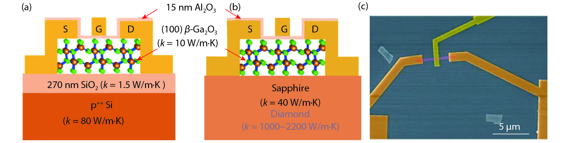
Figs. 25(a), 25(b) and 25(c) show the well-behaved DC IDVDS of three top-gate GOOI FETs with LSD of 6/6.5 μm, LG of 1 μm, and channel thickness of 73/75/74 nm on SiO2/Si, sapphire and diamond substrates, respectively. IDMAX of 960, 535 and 325 mA/mm for diamond, sapphire and SiO2/Si substrates are obtained. IDMAX of GOOI FET on diamond and sapphire substrates is around 3 times and 1.7 times of that on SiO2/Si substrate, originating from better transport properties at a lower device temperature. Fig. 25(d) is the IDVDS comparison at a fixed VGS = 6 V. Figs. 25(e) and 25(f) depict the IDVGS and gmVGS of GOOI FETs on three substrates at VDS = 25 V. High on/off ratio of 109 and low SS of 65 mV/dec are achieved on both devices due to the wide bandgap and high-quality ALD Al2O3/β-Ga2O3 interface, yielding a low interface trap density (Dit) of 2.6 × 10¹¹ eV−1·cm−2 by the equation SS = 60 × (1 + qDit/Cox) mV/dec at room temperature, where Cox is the oxide capacitance. One interesting phenomenon is that the peak gm of diamond and sapphire substrate is 34 mS/mm and 21 mS/mm, which is around 2 times and 60% higher than the gm of SiO2/Si substrate. The extrinsic electron field-effect mobility (μFE) of GOOI FET on diamond, sapphire and SiO2/Si are roughly extracted to be 43, 30.2 and 21.7 cm2/(V·s), respectively, benefiting from the less SHE on diamond.

Figure  25.  (Color online) IDVDS characteristics of GOOI FETs on (a) SiO2/Si, (b) sapphire and (c) diamond substrates with LSD = 6–6.5 μm and LG = 1 μm. A high IDMAX = 960 mA/mm is demonstrated on top-gate β-Ga2O3 GOOI FETs. Comparison of (d) IDVDS (e) log-scale IDVGS and (f) linear-scale gmVGS of β-Ga2O3 FETs on a diamond, sapphire and SiO2/Si substrates. IDVGS transfer characteristics of GOOI FETs on three substrates with high on/off ratio of 109 and low SS of 65 mV/dec, yielding a low Dit of 2.6 × 10¹¹ eV−1·cm−2. Higher gm shows higher electron μ on diamond due to the reduced device temperature. Reprinted from ACS Omega 2,11, 2017. Copyright of 2017 ACS[71] and 2018 IEEE[72].

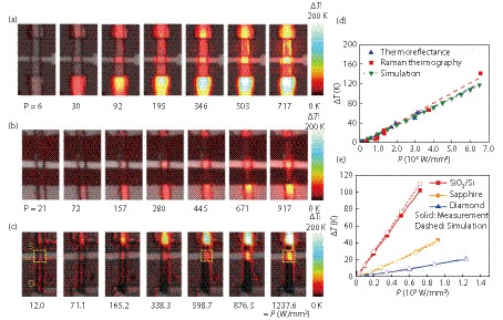
Figs. 26(a), 26(b) and 26(c) are the merged optical and TR thermal image views of GOOI FETs on SiO2/Si, sapphire and diamond substrates at steady state and different P conditions. As higher VDS is applied, the device is heated up simultaneously and the corresponding ΔT is increased. At P = 717 W/mm2 on the SiO2/Si substrate, the ΔT is measured to be 106 K, whereas in contrast the ΔT is just 43 and 21 K at a higher P = 917 W/mm2 and P = 1237 W/mm2 on the sapphire and diamond substrates, respectively. Fig. 26(d) depicts the measured and simulated ΔT versus P (W/mm2) for the Ga2O3 FETs on a diamond substrate, performed both by TR imaging and Raman thermography. Good agreement among these three methods can be observed, with the highest temperature measured by Raman thermography to be 164 °C (ΔT = 141 K) at DC output power of 6565 W/mm2 (64.7 W/mm or VDS = 35 V for this particular exfoliated FET geometry). Fig. 26(e) shows the good agreement of the TR measured and the simulated ΔT versus P (W/mm2) on different substrates. For both the measurement and simulation results, the clear observation is that at the same P, the GOOI FET on the diamond substrate has more than 8 times lower ΔT compared to that on SiO2/Si. The RT of diamond, sapphire and SiO2/Si substrates are calculated to be 1.71 × 10⁻², 4.62 × 10⁻² and 1.47 × 10⁻¹ mm2·K/W, respectively, through RT = ΔT/P. The reduced RT of GOOI FET on diamond and sapphire demonstrate that a higher κ substrate can be more effective in dissipating the heat on the devices. With less heat on the device, the temperature is lower so that the μ is higher to achieve a higher IDMAX of 960 mA/mm for a better device performance.

Figure  26.  (Color online) TR and charge-coupled device (CCD) camera merged images of GOOI FET on (a) SiO2/Si, (b) sapphire and (c) diamond substrates when device P is increased by increasing VDS at VGS = 0 V. (d) Comparison of measured or simulated ΔT versus P (W/mm2) characteristics of top-gate GOOI FETs on a diamond substrate using TR imaging, Raman thermography and the thermal simulations. (e) Measured by TR method and simulated ΔT versus P characteristics of top-gate GOOI FETs on different substrates. The ΔT of GOOI FET on the SiO2/Si substrate is more than 3 and 8 times of that on the sapphire and diamond substrates at the same P. As a result, the RT of GOOI FET on the sapphire substrate is 4.62 × 10⁻² and 1.71 × 10⁻² mm2·K/W, which is less than 1/3 and 1/8 of that on the SiO2/Si substrate. Reprinted from ACS Omega 2,11, 2017. Copyright of 2017 ACS[71].

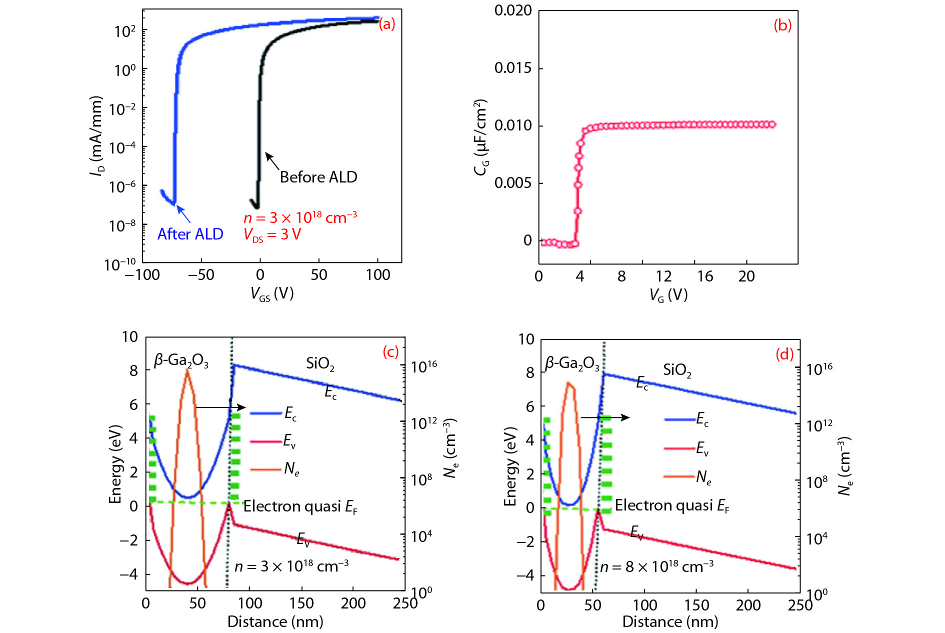
High-temperature solid-state devices and circuits are required for many applications such as in aerospace, automotive, nuclear instrumentations and geothermal wells. Silicon-based complementary metal–oxide–semiconductor (CMOS) technology is not able to operate at such high temperatures, which is limited by its relatively small band gap of 1.12 eV. CMOS circuits using wide band gap semiconductors are promising in these high temperature logic applications. As for the logic application, steep SS is required so as to minimize the power supply so that power consumption and SHE are less severe. In this section, β-Ga2O3 FE-FETs with ferroelectric HZO as a gate dielectric stack is reviewed[74]. Fig. 27(a) shows the schematic diagram of β-Ga2O3 FE-FETs, which consists of a 86 nm thick β-Ga2O3 nanomembrane as the channel, a 3 nm amorphous Al2O3 layer and a 20 nm polycrystalline HZO layer as the gate dielectric, a n++ silicon substrate as the gate electrode, and a Ti/Au source/drain as the metal contacts. Fig. 27(b) shows the false-color SEM image of the fabricated β-Ga2O3 FE-FETs with four different channel lengths, capturing the β-Ga2O3 membrane and the Ti/Au electrodes.
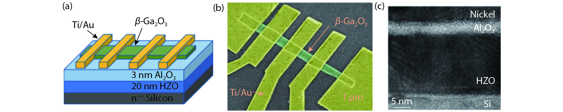
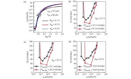
Figure  27.  (Color online) (a) Schematic view of β-Ga2O3 FE-FETs. The gate stack includes a heavily n-doped Si as the gate electrode, 20 nm HZO as the ferroelectric insulator, 3 nm Al2O3 as the capping layer. Ti/Au (30/60 nm) is used as the source/drain electrodes. Sn-doped n-type β-Ga2O3 (86 nm) is used as the channel. (b) Top-view false-color SEM image of representative β-Ga2O3 FE-FETs on the same membrane with different channel lengths. (c) Cross-sectional view of the HZO/Al2O3 gate stack, capturing the polycrystalline HZO and the amorphous Al2O3. Reprinted from ACS Omega 2,10, 2017. Copyright of 2017 ACS[74].

Fig. 28(a) shows the normalized IDVGS characteristics in the log scale of a β-Ga2O3 FE-FET. The back-gate bias is swept from −0.4 to 2 V in 40 mV per step, whereas the VDS is biased at 0.1, 0.5, and 0.9 V. The whole sweep takes roughly 1 min. This device has a LCH of 0.5 μm and a thickness of 86 nm. This particular thickness is chosen to tune the VT slightly above zero. The IDVGS characteristics were measured in bidirectional both forwardly (VGS from low to high) and reversely (VGS from high to low). SS is extracted as a function of ID for both forward sweep (SSmin,For) and reverse sweep (SSmin,Rev) at various VDS. Figs. 28(b)28(d) show the SS–ID characteristics extracted from Fig. 28(a) at VDS = 0.1, 0.5, and 0.9 V, respectively. The device exhibits SSmin,For = 57.2 mV/dec and SSmin,Rev = 41.0 mV/dec at VDS = 0.1 V, SSmin,For = 53.1 mV/dec and SSmin,Rev = 34.3 mV/dec at VDS = 0.5 V, and SSmin,For = 55.0 mV/dec and SSmin,Rev = 34.4 mV/dec at VDS = 0.9 V. SS less than 60 mV/dec at room temperature is demonstrated for both forward and reverse VGS sweeps even at relatively high VDS. Ga2O3 MOSFETs with 15 nm Al2O3 as a gate dielectric exhibit a minimum SS = 118.8 mV/dec. SS–ID characteristics at different VDS are similar, slightly better at high VDS because of the larger impact of a Schottky barrier at lower VDS. Because of the large band gap of β-Ga2O3, the band-to-band tunneling current at high VDS is suppressed. Fig. 29(a) shows the IDVGS characteristics in the linear scale of the same β-Ga2O3 FE-FET as in Fig. 28. VT is extracted by linear extrapolation at VDS = 0.1 V for both forward and reverse VGS sweeps. VT in the forward VGS sweep (VT, For) is extracted as 0.47 V, whereas VT in the reverse VGS sweep (VT, Rev) is extracted as 0.38 V. Hence, the E-mode operation with VT greater than zero for both forward and reverse VGS sweeps is demonstrated. A negligible hysteresis is obtained for both on-state (high VGS, as shown in Fig. 10(a)) and off-state (low VGS, as shown in Fig. 28(a)), except that when VGS is near the VT region. At the VT, low hysteresis is achieved to be 90 mV, calculated by using |VT, RevVT, For|, showing the great promise of using β-Ga2O3 for wide bandgap logic applications.

Figure  28.  (Color online) (a) IDVGS characteristics in the log scale of a β-Ga2O3 FE-FET. This device has a channel length of 0.5 μm and a channel thickness of 86 nm. SS versus ID characteristics of the same device in (a) at (b) VDS = 0.1, (c) VDS = 0.5, and (d) VDS = 0.9 V. SS less than 60 mV/dec at room temperature is demonstrated for both forward and reverse VGS sweeps. Reprinted from ACS Omega 2,10, 2017. Copyright of 2017 ACS[74].
Figure  29.  (Color online) (a) IDVGS characteristics in the linear scale of the same β-Ga2O3 FE-FET as in Fig. 9. (b) IDVDS characteristics of the same β-Ga2O3 FE-FET as in Fig. 9. Reprinted from ACS Omega 2,10, 2017. Copyright of 2017 ACS[74].

In conclusion, significant progresses have been achieved with remarkable power device performances even at this premature development stage, such as BV more than 3 kV of lateral Schottky Rectifiers, high current density 1.5/1 A/mm of D/E-modes FETs, BV of 1.8 kV for field-plated lateral MOSFET and fT/famx of 5.1/17.1 GHz, respectively. In addition to device performance, sufficient low defect density less than 103 cm−2 of melt-grown native substrate and very smooth surface with RMS roughness less than 0.5 nm of epitaxial β-Ga2O3 thin film on its native substrate have all been demonstrated. However, some open questions about how to realize p-type β-Ga2O3 and how to resolve the low thermal conductivity issue are yet to be established. Once resolving those aforementioned issues, the bright future of β-Ga2O3 devices as power electronic products are definitely coming soon.


[1]
Zhang Y, Joishi C, Xia Z et al. Demonstration of β-(AlxGa1-x)2O3/Ga2O3 double heterostructure field effect transistors. Appl Phys Lett 2018, 112: 233503 doi: 10.1063/1.5037095
[2]
Lv Y, Zhou X, Long S et al. Source-Field-Plated β-Ga2O3 MOSFET with Record Power Figure of Merit of 50.4 MW/cm2. IEEE Electron Device Lett 2019, 39 doi: 10.1109/LED.2018.2881274
[3]
Green A J, Chabak K, Heller E R, et al. 3.8 MV/cm Breakdown strength of MOVPE-grown Sn-doped Ga2O3 MOSFETs. IEEE Electron Device Lett, 2016, 37 (7): 902. doi: 10.1109/LED.2016.2568139
[4]
Chabak K D, Moser N, Green A J, et al. Enhancement-mode Ga2O3 wrap-gate fin field-effect transistors on native (100) β-Ga2O3 substrate with high breakdown voltage. Appl Phys Lett, 2016, 109: 213501. doi: 10.1063/1.4967931
[5]
Tadjer M, Mahadik N, Wheeler V D, et al. Communications-A (001) β-Ga2O3 MOSFETs with +2.9 V threshold voltage and HfO2 gate dielectric. ECS J Solid State Sci Tech, 2016, 5: 468. doi: 10.1149/2.0061609jss
[6]
Zeng K, Wallace J S, Heimburger C, et al. Ga2O3 MOSFETs using spin-on-glass source/drain doping technology. IEEE Electron Device Lett, 2017, 38 (4): 513. doi: 10.1109/LED.2017.2675544
[7]
Wort C J H, Balmer R S. Diamond as an electronic material. Mater Today, 2008, 11 (1): 22. doi: 10.1016/S1369-7021(07)70349-8
[8]
Fu H, Baranowski I, Huang X, et al. Demonstration of AlN Schottky barrier diodes with blocking voltage over 1 kV. IEEE Electron Device Lett, 2017, 38 (9): 1286. doi: 10.1109/LED.2017.2723603
[9]
Baliga B J. Power semiconductor-device figure of merit for high-frequency applications. IEEE Electron Device Lett, 1989, 10(10): 455. doi: 10.1109/55.43098
[10]
Wenckstern H V. Group‐III sesquioxides: growth, physical properties and devices. Adv Electron Mater, 2017, 3(9): 1600350. doi: 10.1002/aelm.v3.9
[11]
Yoshioka S, Hayashi H, Kuwabara A, et al. Structures and energetics of Ga2O3 polymorphs. J Phys: Condens Matter, 2007, 19: 346211. doi: 10.1088/0953-8984/19/34/346211
[12]
He H, Orlando R, Blanco M A, et al. First-principles study of the structural, electronic, and optical properties of Ga2O3 in its monoclinic and hexagonal phases. Phys Rev B, 2006, 74 (19): 195123. doi: 10.1103/PhysRevB.74.195123
[13]
He H, Blanco M A, Pandey R. Electronic and thermodynamic properties of Ga2O3. Appl Phys Lett, 2006, 88: 261904. doi: 10.1063/1.2218046
[14]
Kroll P, Dronskowski R, Martin M. Formation of spinel-type gallium oxynitrides: a density-functional study of binary and ternary phases in the system Ga–O–N. J Mater Chem, 2005, 15: 3296. doi: 10.1039/b506687e
[15]
Playford H Y, Hannon A C, Barney E R, et al. Structures of Uncharacterised Polymorphs of Gallium Oxide from Total Neutron Diffraction. Eur J, 2013, 19 (8): 2803. doi: 10.1002/chem.201203359
[16]
Peelaers H, Van de Walle C G. Brillouin zone and band structure of β‐Ga2O3. Phys Status Solidi B, 2015, 252 (4): 828. doi: 10.1002/pssb.201451551
[17]
Varley J B, Weber J R, Janotti A, et al. Oxygen vacancies and donor impurities in β-Ga2O3. Appl Phys Lett, 2010, 97: 142106. doi: 10.1063/1.3499306
[18]
Vasyltsiv V I, Rym Y I, Zakharo Y M. Optical absorption and photoconductivity at the band edge of β‐Ga2−xInxO3. Phys Status Solidi B, 1996, 195, 653. doi: 10.1002/(ISSN)1521-3951
[19]
Galazka Z, Irmscher K, Uecker R, et al. On the bulk β-Ga2O3 single crystals grown by the Czochralski method. J Cryst Growth, 2014, 404 (15): 184. doi: 10.1016/j.jcrysgro.2014.07.021
[20]
Galazka Z, Uecker R, Irmscher K, et al. Czochralski growth and characterization of β‐Ga2O3 single crystals. Cryst Res Technol, 2010, 45 (12), 1229. doi: 10.1002/crat.v45.12
[21]
Kuramata A, Koshi K, Watanabe S, et al. High-quality β-Ga2O3 single crystals grown by edge-defined film-fed growth. Jpn J App Phys Part 1, 2016, 55, 1202A2. doi: 10.7567/JJAP.55.1202A2
[22]
Vıllora E G, Morioka Y, Atou T. Infrared reflectance and electrical conductivity of β-Ga2O3. Phys. Status Solidi A, 2002, 193: 187. doi: 10.1002/(ISSN)1521-396X
[23]
Zhang J, Li B, Xia C, Growth and spectral characterization of β-Ga2O3 single crystals. J Phys Chem Solids, 2006, 67: 2448. doi: 10.1016/j.jpcs.2006.06.025
[24]
Suzuki N, Ohira S, Tanaka M. Fabrication and characterization of transparent conductive Sn-doped β-Ga2O3 single crystal. Phys Status Solidi C, 2007, 4 (7): 2310. doi: 10.1002/(ISSN)1610-1642
[25]
Mohamed M, Irmscher K, Janowitz C, et al. Schottky barrier height of Au on the transparent semiconducting oxide β-Ga2O3. Appl Phys Lett, 2012, 101: 132106. doi: 10.1063/1.4755770
[26]
Suzuki K, Okamoto T, Takata M. Crystal growth of β-Ga2O3 by electric current heating method. Ceram Int, 2004, 30(7): 1679. doi: 10.1016/j.ceramint.2003.12.154
[27]
Zhang J, Xia C, Deng Q, et al. Growth and characterization of new transparent conductive oxides single crystals β-Ga2O3: Sn. J Phys Chem Solids, 2006, 67: 1656. doi: 10.1016/j.jpcs.2006.02.018
[28]
Tomm Y, Reiche P, Klimm D, et al. Czochralski grown Ga2O3 crystals. J Cryst Growth, 2000, 220 (4): 510. doi: 10.1016/S0022-0248(00)00851-4
[29]
Galazka Z, Uecker R, Klimm D et al.Scaling-Up of Bulk β-Ga2O3 Single Crystals by the Czochralski Method. ECS J Solid State Sci Technol 2017, 6: Q3007 doi: 10.1016/j.jcrysgro.2014.07.021
[30]
Higashiwaki M, Kuramata A, Murakami H, et al. State-of-the-art technologies of gallium oxide power devices. J Phys D, 2017, 50: 333002. doi: 10.1088/1361-6463/aa7aff
[31]
Hoshikawa K, Ohba E, Kobayashi E, et al. Growth of β-Ga2O3 single crystals using vertical Bridgman method in ambient air. J Cryst Growth, 2016, 447 (1): 36. doi: 10.1016/j.jcrysgro.2016.04.022
[32]
Alema F, Hertog B, Osinsky A, et al. Fast growth rate of epitaxial β–Ga2O3 by close coupled showerhead MOCVD. J Cryst Growth, 2017, 475: 77. doi: 10.1016/j.jcrysgro.2017.06.001
[33]
Gogova D, Wagner G, Baldini M, et al. Structural properties of Si-doped β-Ga2O3 layers grown by MOVPE. J Cryst Growth, 2014, 401: 665. doi: 10.1016/j.jcrysgro.2013.11.056
[34]
Baldini M, Albrecht M, Fiedler A, et al. Semiconducting Sn-doped β-Ga2O3 homoepitaxial layers grown by metal organic vapour-phase epitaxy. J Mater Sci, 2016, 51(7): 3650. doi: 10.1007/s10853-015-9693-6
[35]
Sasaki K, Higashiwaki M, Kuramata A, et al. Growth temperature dependences of structural and electrical properties of Ga2O3 epitaxial films grown on β-Ga2O3 (010) substrates by molecular beam epitaxy. J Cryst Growth, 2014, 392: 30. doi: 10.1016/j.jcrysgro.2014.02.002
[36]
Oshima T, Okuno T, Fujita S. Ga2O3 thin film growth on c-plane sapphire substrates by molecular beam epitaxy for deep-ultraviolet photodetectors. Jpn J Appl Phys, 2007, 46: 7217. doi: 10.1143/JJAP.46.7217
[37]
Okumura H, Kita M, Sasaki K, et al. Systematic investigation of the growth rate of β-Ga2O3(010) by plasma-assisted molecular beam epitaxy. Appl Phys Express, 2014, 7: 095501. doi: 10.7567/APEX.7.095501
[38]
Oshima T, Arai N, Suzuki N, et al. Surface morphology of homoepitaxial β-Ga2O3 thin films grown by molecular beam epitaxy. Thin Solid Films, 2008, 516: 5768. doi: 10.1016/j.tsf.2007.10.045
[39]
Y Oshima, E G Vıllora, K Shimamura. Halide vapor phase epitaxy of twin-free α-Ga2O3 on sapphire (0001) substrates. Appl Phys Express, 2015, 8: 055501. doi: 10.7567/APEX.8.055501
[40]
Watahiki T, Yuda Y, Furukawa A, et al. Heterojunction p-Cu2O/n-Ga2O3 diode with high breakdown voltage. Appl Phys Lett, 2017, 111: 222104. doi: 10.1063/1.4998311
[41]
Murakami H, Nomura K, Goto K, et al. Homoepitaxial growth of β-Ga2O3 layers by halide vapor phase epitaxy. Appl Phys Express, 2015, 8: 015503. doi: 10.7567/APEX.8.015503
[42]
K Nomura, K Goto, R Togashi, et al. Thermodynamic study of β-Ga2O3 growth by halide vapor phase epitaxy. J Cryst Growth, 2014, 405: 19. doi: 10.1016/j.jcrysgro.2014.06.051
[43]
Hebert C, Petitmangin A, Perrie're J, et al. Phase separation in oxygen deficient gallium oxide films grown by pulsed-laser deposition. Mater Chem Phys, 2012, 133 (1): 135. doi: 10.1016/j.matchemphys.2011.12.078
[44]
Chen Z, Wang X, Noda S, et al. Effects of dopant contents on structural, morphological and optical properties of Er doped Ga2O3 films. Superlattices Microstruct, 2016, 90: 207. doi: 10.1016/j.spmi.2015.12.025
[45]
Kawaharamura T. Physics on development of open-air atmospheric pressure thin film fabrication technique using mist droplets: Control of precursor flow. Jpn J Appl Phys, 2014, 53: 05FF08. doi: 10.7567/JJAP.53.05FF08
[46]
Lee S D, Kaneko K, Fujita S. Homoepitaxial growth of beta gallium oxide films by mist chemical vapor deposition. Jpn J Appl Phys, 2016, 55: 1202B8. doi: 10.7567/JJAP.55.1202B8
[47]
Dang G T, Kawaharamura T, Furuta M, et al. Metal–semiconductor field-effect transistors with In–Ga–Zn–O channel grown by nonvacuum-processed mist chemical vapor deposition. IEEE Electron Device Lett, 2015, 36 (5): 463. doi: 10.1109/LED.2015.2412124
[48]
Fujita S, Kaneko K. Epitaxial growth of corundum-structured wide band gap III-oxide semiconductor thin films. J Cryst Growth, 2014, 401: 588. doi: 10.1016/j.jcrysgro.2014.02.032
[49]
Akaiwa K, Fujita S. Electrical conductive corundum-structured α-Ga2O3 thin films on sapphire with tin-doping grown by spray-assisted mist chemical vapor deposition. Jpn J Appl Phys, 2012, 51: 070203. doi: 10.1143/JJAP.51.070203
[50]
Baldini M, Albrecht M, Gogova D, et al. Effect of indium as a surfactant in (Ga1−xInx)2O3 epitaxial growth on β-Ga2O3 by metal organic vapour phase epitaxy. Semicond Sci Technol, 2015, 30: 024013. doi: 10.1088/0268-1242/30/2/024013
[51]
Hu Z, Zhou H, Feng Q. Field-plated lateral β-Ga2O3 Schottky barrier diode with high reverse blocking voltage of more than 3 kV and high power figure-of-merit of 500 MW/cm2. IEEE Electron Device Lett, 2018, 39(10): 1564. doi: 10.1109/LED.2018.2868444
[52]
Sasaki K, Kuramata A, Masui T, et al. Device-quality beta-Ga2O3 epitaxial films fabricated by ozone molecular beam epitaxy. Appl Phys Exp, 2012, 5: 035502. doi: 10.1143/APEX.5.035502
[53]
Konishi K, Goto K, Murakami H, et al. 1-kV vertical β-Ga2O3 field-plated Schottky barrier diodes. Appl Phys Lett, 2017, 110 (10): 103506. doi: 10.1063/1.4977857
[54]
Yang J, Ahn S, Ren F, et al. High reverse breakdown voltage Schottky rectifiers without edge termination on β-Ga2O3. Appl Phys Lett, 2017, 110 (19): 192101. doi: 10.1063/1.4983203
[55]
Yang J, Ahn S, Ren F, et al. High breakdown voltage (−201) β-Ga2O3 Schottky rectifiers. IEEE Electron Device Lett, 2017, 38 (7): 906. doi: 10.1109/LED.2017.2703609
[56]
Yang J, Ren F, Pearton S J, et al. Vertical geometry 2-A forward current Ga2O3 Schottky rectifiers on bulk Ga2O3 substrates. IEEE Trans Electron Devices, 2018, 65(7): 2790. doi: 10.1109/TED.2018.2838439
[57]
Higashiwaki M, Sasaki K, Kuramata A, et al. Gallium oxide (Ga2O3) metal−semiconductor field-effect transistors on single-crystal β-Ga2O3 (010) substrates. Appl Phys Lett 2012, 100: 013504. doi: 10.1063/1.3674287
[58]
Wong M H, Sasaki K, Kuramata A, et al. Field-plated Ga2O3 MOSFETs with a breakdown voltage of over 750 V. IEEE Electron Device Lett, 2016, 37: 212. doi: 10.1109/LED.2015.2512279
[59]
Zeng K, Vaidya A, Singisetti U, et al. 1.85 kV breakdown voltage in lateral field-plated Ga2O3 MOSFETs. IEEE Electron Device Lett, 2018, 39(9): 1385. doi: 10.1109/LED.2018.2859049
[60]
Zeng K, Sasaki K, Kuramata A, et al. Depletion and enhancement mode β-Ga2O3 MOSFETs with ALD SiO2 gate and near 400 V breakdown voltage. Proc 74th Annu DRC, 2016: 1
[61]
Hu Z, Nomoto K, Li W, et al. Enhancement-mode Ga2O3 vertical transistors with breakdown voltage >1 kV. IEEE Electron Device Lett, 2018, 39(6): 869. doi: 10.1109/LED.2018.2830184
[62]
Green A J, Chabak K D, Baldini M, et al. β-Ga2O3 MOSFETs for radio frequency operation. IEEE Electron Device Lett, 2017.38 (6): 790. doi: 10.1109/LED.2017.2694805
[63]
Singh M, Casbon M A, Uren M J, et al. Pulsed large signal rf performance of field-plated Ga2O3 MOSFETs. IEEE Electron Device Lett, 2018.39 (10): 1572. doi: 10.1109/led.2018.2865832
[64]
Chabak K D, Walker D E, Green A J, et al. sub-micron gallium oxide radio frequency field-effect transistors. IEEE MTT-S IMWS-AMP, 2018: 1
[65]
Hwang W S, Verma A, Peelaers H, et al. High-voltage field effect transistors with wide-bandgap beta-Ga2O3 nanomembranes. Appl Phys Lett, 2014, 104: 203111. doi: 10.1063/1.4879800
[66]
Hu Z, Zhou H, Dang K, et al. lateral-ga2o3 schottky barrier diode on sapphire substrate with reverse blocking voltage of 1.7 kV. IEEE J Electron Device Soc, 2018, 6: 815. doi: 10.1109/JEDS.2018.2853615
[67]
Zhou H, Maize K, Qiu G, et al. β-Ga2O3 on insulator field-effect transistors with drain currents exceeding 1.5 A/mm and their self-heating effect. Appl Phys Lett, 2017, 111: 092102. doi: 10.1063/1.5000735
[68]
: Zhou H, Si M, Alghamdi S, et al. High performance depletion/ enhancement mode β-Ga2O3 on insulator (GOOI) field-effect transistors with record drain currents of 600/450 mA/mm. IEEE Electron Device Lett, 2017, 38: 103. doi: 10.1109/LED.2016.2635579
[69]
Moser N A, Mccandless J P, Crespo A, et al. High pulsed density β-Ga2O3 MOSFETs verified by an analytical model corrected for interface charge. Appl Phys Lett, 2017, 110: 143505. doi: 10.1063/1.4979789
[70]
Shin S H, Wahab M A, Masuduzzaman A, et al. Direct observation of self-heating in III–V gate-all-around nanowire MOSFETs. IEEE Trans Electron Devices, 2014, 62: 3516. doi: 10.1109/IEDM.2014.7047088
[71]
Zhou H, Maize K, Noh J, et al. Thermo-dynamic studies of β-Ga2O3 nano-membrane field-effect transistors on sapphire substrate. ACS Omega, 2017, 2: 7723. doi: 10.1021/acsomega.7b01313
[72]
Noh J, Si M, Zhou H, et al. The impact of substrates on the performance of top-gate β-Ga2O3 field-effect transistors: record high drain current of 980 mA/mm on diamond. IEEE Device Research Conference, 2018: 1.
[73]
Maize K, Zibari A, French W D, et al. Thermoreflectance ccd imaging of self-heating in power MOSFET arrays. IEEE Trans Electron Devices 2014, 61: 3047. doi: 10.1109/TED.2014.2332466
[74]
Si M, Yang L, Zhou H, et al. β-Ga2O3 Nanomembrane negative capacitance field-effect transistors with steep subthreshold slope for wide band gap logic applications. ACS Omega, 2017, 2: 7136. doi: 10.1021/acsomega.7b01289
Fig. 1.  (Color online) Atomic unit cell of β-Ga2O3 with lattice constant and angle marked.

Fig. 2.  Band structure of β-Ga2O3 with Fermi energy aligned to zero. Reprint from Appl Phys Lett, 88, 261904 (2006). Copyright 2006 American Institute of Physics.

Fig. 3.  Photograph of 4-inch-diameter β-Ga2O3 wafer. Reprinted from Higashiwaki et al., J Phy D, 50 (2017). Copyright 2017 IOP Publishing[30].

Fig. 4.  (Color online) β-Ga2O3 crystals grown by the VB method in either (a) a full-diameter crucible (a’), and (b) or in a conical crucible (b’). Reprinted from Hoshikawa et al., J Cryst Growth 447, 36 (2016). Copyright 2016 Elsevier[31].

Fig. 5.  (Color online) (a) HRTEM image of an undoped homoepitaxial β-Ga2O3 layer from MOVPE method. (b) Surface morphologies of 60-nm-thick β-Ga2O3 (010) layers grown on Sn-doped β-Ga2O3 (010) substrates at a growth rate of 1 nm/min under slightly Ga-rich conditions at the growth temperatures of 500, 700, 800, and 900 °C, respectively. NDIC microscopy images of β-Ga2O3 surfaces after HVPE growth on (001) β-Ga2O3 substrates for 1 h at (c) 800 and (d) 1000 °C. Reprinted from Refs. [33, 37, 41].

Fig. 6.  (Color online) (a) Electron mobility as a function of carrier concentration. (b) I–V characteristics of Pt/β-Ga2O3 Schottky barrier diodes. The inset shows the schematic structure of the β-Ga2O3 SBD. Reprinted from Sasaki et al., Appl Phys Express, 5, 035502 (2012)[52]. Copyright of 2012 Japanese Society of Applied Physics.

Fig. 7.  (Color online) (a) Forward and (b) reverse J–V characteristics of β-Ga2O3 FP-SBD at room temperature. Inset shows the cross-section device schematic of the vertical SBD. Reprinted from Appl Phys Lett, 110, 103506 (2017). Copyright 2017 American Institute of Physics[53].

Fig. 8.  (Color online) (a) Reverse I–V characteristics of 3 diodes with two different diameters, showing a diameter dependence of the BV, and (b) forward and reverse I–V characteristics from a 20 μm diameter diode. Reprinted from Appl Phys Lett, 110, 192101 (2017) and IEEE Electron Device Lett. Copyrights 2017 American Institute of Physics and 2017 IEEE[54, 55].

Fig. 9.  (Color online) (a) DC output characteristics of β-Ga2O3 MESFET and (b) transfer characteristics of the same MESFET at VDS = 40 V. Reprinted from Appl Phys Lett, 100, 013504 (2012). Copyrights 2012 American Institute of Physics[57].

Fig. 10.  (Color online) (a) Schematic cross section of a β-Ga2O3 MOSFET with a gate-connected FP structure and (b) Output characteristics of the MOSFET with maximum ID of 78 mA/mm and BV of 750 V. Reprinted from IEEE Electron Device Lett, 37, 2 (2016). Copyright of 2016 IEEE[58].

Fig. 11.  (Color online) (a) Cross-section view and (b) optical image of the fabricated field-plated Ga2O3 MOSFET with SOG S/D doping. (c) Three-terminal breakdown measurement of the field-plated Ga2O3 MOSFET and a record-high BV of 1850 V is demonstrated. Reprinted from IEEE Electron Device Lett, 39, 9 (2018). Copyright of 2018 IEEE[59].

Fig. 12.  (Color online) IDVGS characteristics of (a) Zeng’s and (b) Tadjer’s E-mode MOSFET. Reprinted from IEEE Device Research Conf and ECS J, Solid State Sci, Technol, 39, 9 (2018). Copyright of 2016 IEEE[60] and 2016 ECS[5].

Fig. 13.  (Color online) (a) Tilted false-colored SEM image of a fabricated E-mode β-Ga2O3 Fin-MOSFET and (b) The breakdown characteristics of β-Ga2O3 Fin-MOSFET with LG = 2 μm and LGD = 16, 21 μm at VGS = 0 V. The inset shows the transfer characteristics of the same device indicating a VTH = 0.8 V. Reprinted from Appl Phys Lett, 109, 213501 (2016). Copyrights 2016 American Institute of Physics[4].

Fig. 14.  (Color online) (a) Schematic cross-section and (b) SEM image of a vertical E-mode β-Ga2O3 Fin-MOSFET, (c) transfer characteristics of the device with a VTH = 2.2 V, on/off ratio of 108, and on-current of 400 A/cm2. (d) The breakdown characteristics of β-Ga2O3 Fin-MOSFET with channel width of 330 nm. Reprinted from IEEE Electron Device Lett, 39, 869, 2018. Copyright of 2018 IEEE[61].

Fig. 15.  (Color online) (a) A device cross section schematic is shown for the β-Ga2O3 MOSFET under test. (b) A focused ion beam (FIB) cross sectional image of the device. (c) Extrinsic small signal RF gain performance recorded at VGS = −3.5 V (peak gm) and VDS = 40 V (d) 800 MHz Class-A power sweep of a 2 × 50 μm β-Ga2O3 gate recessed MOSFET. Reprinted from IEEE Electron Device Lett, 38, 790, 2017. Copyright of 2017 IEEE[62].

Fig. 16.  (Color online) (a) DC output characteristics and pulsed IV from a quiescent bias of VGS = VDS = 0 V up to VDS = 80 V with 1 μs pulse length and 1 ms period (b) Pulsed and CW large signal measurements at 1 GHz with input available power sweep up to 22 dBm, measured at VDS = 40 V with IDS = 5 mA. Reprinted from IEEE Electron Device Lett, 39, 1572, 2018. Copyright of 2018 IEEE[63].

Fig. 17.  (Color online) Transfer characteristics of the thin-channel BGO MOSFET with T-gate. The GM reaches 25 mS/mm with current density over 275 mA/mm, and the inset shows a good ION/IOFF ratio greater than 108. (b) Small signal gain at VDS = 15 V of the thin-channel BGO MOSFET with ft/fmax = 5.1/17.1 GHz. Reprinted from IEEE IMWS-AMP, 2018. Copyright of 2018 IEEE[64].

Fig. 18.  (Color online) (a) Schematic-view and (b) top-view microscopy image of a fabricated lateral β-Ga2O3 SBD on sapphire substrate. (c) Log-scale forward characteristics of β-Ga2O3 SBD with LSchottky-Ohmic = 15 μm at the temperature range from 30 to 150 °C with 20 °C as a step. (d) Linear-scale forward I–V characteristics of β-Ga2O3 SBDs with various LSchottky−Ohmic. (e) Reverse I–V characteristics of lateral β-Ga2O3 SBDs with various LSchottky−Ohmic. Reprinted from IEEE JEDS 6, 815, 2018. Copyright of 2018 IEEE[66].

Fig. 19.  (Color online) (a) Tilted 3-D schematic-view and (b) top-view microscopy image of a fabricated lateral field-plated β-Ga2O3 SBD on Sapphire substrate. (c) Forward I–V and differential RonV characteristics in linear scale. The inset shows as-measured current dependence on the width of the SBD at a similar LAC of 14–18 μm. (d) Reverse I–V characteristics of lateral SBDs with field plate structure and various LAC. (e) DC RON,SP versus BV of some both lateral and vertical β-Ga2O3 SBDs. Reprinted from IEEE Electron Device Lett, 39, 1564, 2018. Copyright of 2018 IEEE[51].

Fig. 20.  (Color online) (a) Schematic view of a GOOI FET with a 300 nm SiO2 layer on Si substrate and (b) AFM image of the atomic flat β-Ga2O3 surface after cleavage. Reprinted from IEEE Electron Device Lett, 38, 103, 2017. Copyright of 2017 IEEE[68].

Fig. 21.  (Color online) (a) and (c) are IDVDS output characteristics of D- and E-mode GOOI FETs with 3.0 × 10¹⁸ and 8.0 × 1018 cm−3 doping channel, respectively. (b) and (d) are IDgmVGS transfer characteristics of D-mode and E-mode GOOI FETs with 8.0 × 1018 cm−3 doping channel, respectively. Record high IDMAX of 1.5 and 1.0 A/mm are demonstrated for D/E mode devices. Both D and E-mode devices have high on/off ratio of 1010 and low SS of 150–165 mV/dec for 300 nm SiO2. Reprinted from Appl Phys Lett, 111, 092102, 2017. Copyright of 2017 AIP[67].

Fig. 22.  (Color online) (a) Thickness dependent IDVGS plots of various GOOI FETs from D-mode of thicker β-Ga2O3 to E-mode of thinner β-Ga2O3. (b) Thickness dependent VT extracted at VDS = 1 V of 15 devices. Reprinted from IEEE Electron Device Lett, 38, 103, 2017. Copyright of 2017 IEEE[68].

Fig. 23.  (Color online) (a) IDVGS comparison between GOOI FETs with and without ALD passivation for β-Ga2O3 nano-membrane with doping concentration of 3.0 × 1018 cm−3, (b) simulated C–V curve for E-mode GOOI FET at a β-Ga2O3 nano-membrane thickness of 80 nm and doping concentration of 3.0 × 1018 cm−3 after considering the top and bottom negative surface charge (ns = 1.2 × 1013 cm2) depletion effect. Band diagram and electron density distribution of E-mode GOOI FETs with surface negative charge depletion on (c) lower doping (ns = 1.2 × 1013 cm−2) and (d) high doping (ns = 2.2 × 1013 cm−2) β-Ga2O3 nano-membrane channels at VGS = 0 V. Reprinted from Appl Phys Lett, 111, 092102, 2017. Copyright of 2017 AIP[67].

Fig. 24.  (Color online) Cross-section schematic view of a top-gate GOOI FET on (a) SiO2/Si and (b) sapphire and diamond substrates with different κ marked. 15 nm of Al2O3 is used as the gate dielectric, Ti/Al/Au (15/60/50 nm) is used as the source/drain electrodes, and Ni/Au (30/50 nm) is used the gate electrode. (c) False-colored SEM top-view of a GOOI FET with LG = 1 μm and LSD = 6 μm. Reprinted from ACS Omega 2,11, 2017. Copyright of 2017 ACS[71].

Fig. 25.  (Color online) IDVDS characteristics of GOOI FETs on (a) SiO2/Si, (b) sapphire and (c) diamond substrates with LSD = 6–6.5 μm and LG = 1 μm. A high IDMAX = 960 mA/mm is demonstrated on top-gate β-Ga2O3 GOOI FETs. Comparison of (d) IDVDS (e) log-scale IDVGS and (f) linear-scale gmVGS of β-Ga2O3 FETs on a diamond, sapphire and SiO2/Si substrates. IDVGS transfer characteristics of GOOI FETs on three substrates with high on/off ratio of 109 and low SS of 65 mV/dec, yielding a low Dit of 2.6 × 10¹¹ eV−1·cm−2. Higher gm shows higher electron μ on diamond due to the reduced device temperature. Reprinted from ACS Omega 2,11, 2017. Copyright of 2017 ACS[71] and 2018 IEEE[72].

Fig. 26.  (Color online) TR and charge-coupled device (CCD) camera merged images of GOOI FET on (a) SiO2/Si, (b) sapphire and (c) diamond substrates when device P is increased by increasing VDS at VGS = 0 V. (d) Comparison of measured or simulated ΔT versus P (W/mm2) characteristics of top-gate GOOI FETs on a diamond substrate using TR imaging, Raman thermography and the thermal simulations. (e) Measured by TR method and simulated ΔT versus P characteristics of top-gate GOOI FETs on different substrates. The ΔT of GOOI FET on the SiO2/Si substrate is more than 3 and 8 times of that on the sapphire and diamond substrates at the same P. As a result, the RT of GOOI FET on the sapphire substrate is 4.62 × 10⁻² and 1.71 × 10⁻² mm2·K/W, which is less than 1/3 and 1/8 of that on the SiO2/Si substrate. Reprinted from ACS Omega 2,11, 2017. Copyright of 2017 ACS[71].

Fig. 27.  (Color online) (a) Schematic view of β-Ga2O3 FE-FETs. The gate stack includes a heavily n-doped Si as the gate electrode, 20 nm HZO as the ferroelectric insulator, 3 nm Al2O3 as the capping layer. Ti/Au (30/60 nm) is used as the source/drain electrodes. Sn-doped n-type β-Ga2O3 (86 nm) is used as the channel. (b) Top-view false-color SEM image of representative β-Ga2O3 FE-FETs on the same membrane with different channel lengths. (c) Cross-sectional view of the HZO/Al2O3 gate stack, capturing the polycrystalline HZO and the amorphous Al2O3. Reprinted from ACS Omega 2,10, 2017. Copyright of 2017 ACS[74].

Fig. 28.  (Color online) (a) IDVGS characteristics in the log scale of a β-Ga2O3 FE-FET. This device has a channel length of 0.5 μm and a channel thickness of 86 nm. SS versus ID characteristics of the same device in (a) at (b) VDS = 0.1, (c) VDS = 0.5, and (d) VDS = 0.9 V. SS less than 60 mV/dec at room temperature is demonstrated for both forward and reverse VGS sweeps. Reprinted from ACS Omega 2,10, 2017. Copyright of 2017 ACS[74].

Fig. 29.  (Color online) (a) IDVGS characteristics in the linear scale of the same β-Ga2O3 FE-FET as in Fig. 9. (b) IDVDS characteristics of the same β-Ga2O3 FE-FET as in Fig. 9. Reprinted from ACS Omega 2,10, 2017. Copyright of 2017 ACS[74].

Table 1.   Properties of β-Ga2O3 relative to some other major semiconductors used for power electronics applications, considering their different kinds of FOM.

Material Parameter Si GaAs 4H-SiC GaN Diamond β-Ga2O3
Bandgap Eg (eV) 1.14 1.43 3.25 3.4 5.5 4.8
Dielectric constant ε 12 13 10 9 5.5 11
Breakdown field EC (MV/cm) 0.3 0.4 2.5 3.3 10 8
Carrier mobility μ (cm2/(V·s)) 1450 8400 1000 1200 2000 300
Saturation velocity νsat (107 cm/s) 1 1.2 2 2.5 1 2
Thermal conductivity κ (W/mK) 150 50 370 250 2000 10–30
FOM relative to Si
Baliga FOM = εμEc3 1 14.7 317 846 24 660 3200
Johnson FOM = Ec2νsat2/4π2 1 1.8 278 1089 1110 2844
Baliga High Frequency FOM = μEc2 1 10 46 100 1500 142
Keyes FOM = κ[(sat)(4πε)]1/2 1 0.3 3.6 1.8 41.5 0.2
DownLoad: CSV

Table 2.   Comparison of CW and pulse large signal measurements performed at two different operating power levels of 0.4 and 0.8 W/mm. larger differences in performance between cw and pulsed modes can been seen with increasing operating power. Reprinted from IEEE Electron Device Lett, 39, 1572, 2018. Copyright of 2018 IEEE.

Parameter Operating condition 0.4 W/mm 25 °C
(IDS = 5 mA, Vds = 40 V)
Operating condition 0.8 W/mm 25 °C
(IDS = 10 mA, VDS = 40 V)
CW Pulse CW Pulse
Pout (dBm) 17.42 18.28 17.63 19.52
Pout (W/mm) 0.11 0.13 0.11 0.17
Drain Eff (%) 19.56 22.40 13.83 17.04
PAE (%) 9.09 12.01 3.23 6.85
Max gain (dB) 4.17 4.81 2.08 3.68
Channel temperature (°C) 58 28 97 36
DownLoad: CSV
[1]
Zhang Y, Joishi C, Xia Z et al. Demonstration of β-(AlxGa1-x)2O3/Ga2O3 double heterostructure field effect transistors. Appl Phys Lett 2018, 112: 233503 doi: 10.1063/1.5037095
[2]
Lv Y, Zhou X, Long S et al. Source-Field-Plated β-Ga2O3 MOSFET with Record Power Figure of Merit of 50.4 MW/cm2. IEEE Electron Device Lett 2019, 39 doi: 10.1109/LED.2018.2881274
[3]
Green A J, Chabak K, Heller E R, et al. 3.8 MV/cm Breakdown strength of MOVPE-grown Sn-doped Ga2O3 MOSFETs. IEEE Electron Device Lett, 2016, 37 (7): 902. doi: 10.1109/LED.2016.2568139
[4]
Chabak K D, Moser N, Green A J, et al. Enhancement-mode Ga2O3 wrap-gate fin field-effect transistors on native (100) β-Ga2O3 substrate with high breakdown voltage. Appl Phys Lett, 2016, 109: 213501. doi: 10.1063/1.4967931
[5]
Tadjer M, Mahadik N, Wheeler V D, et al. Communications-A (001) β-Ga2O3 MOSFETs with +2.9 V threshold voltage and HfO2 gate dielectric. ECS J Solid State Sci Tech, 2016, 5: 468. doi: 10.1149/2.0061609jss
[6]
Zeng K, Wallace J S, Heimburger C, et al. Ga2O3 MOSFETs using spin-on-glass source/drain doping technology. IEEE Electron Device Lett, 2017, 38 (4): 513. doi: 10.1109/LED.2017.2675544
[7]
Wort C J H, Balmer R S. Diamond as an electronic material. Mater Today, 2008, 11 (1): 22. doi: 10.1016/S1369-7021(07)70349-8
[8]
Fu H, Baranowski I, Huang X, et al. Demonstration of AlN Schottky barrier diodes with blocking voltage over 1 kV. IEEE Electron Device Lett, 2017, 38 (9): 1286. doi: 10.1109/LED.2017.2723603
[9]
Baliga B J. Power semiconductor-device figure of merit for high-frequency applications. IEEE Electron Device Lett, 1989, 10(10): 455. doi: 10.1109/55.43098
[10]
Wenckstern H V. Group‐III sesquioxides: growth, physical properties and devices. Adv Electron Mater, 2017, 3(9): 1600350. doi: 10.1002/aelm.v3.9
[11]
Yoshioka S, Hayashi H, Kuwabara A, et al. Structures and energetics of Ga2O3 polymorphs. J Phys: Condens Matter, 2007, 19: 346211. doi: 10.1088/0953-8984/19/34/346211
[12]
He H, Orlando R, Blanco M A, et al. First-principles study of the structural, electronic, and optical properties of Ga2O3 in its monoclinic and hexagonal phases. Phys Rev B, 2006, 74 (19): 195123. doi: 10.1103/PhysRevB.74.195123
[13]
He H, Blanco M A, Pandey R. Electronic and thermodynamic properties of Ga2O3. Appl Phys Lett, 2006, 88: 261904. doi: 10.1063/1.2218046
[14]
Kroll P, Dronskowski R, Martin M. Formation of spinel-type gallium oxynitrides: a density-functional study of binary and ternary phases in the system Ga–O–N. J Mater Chem, 2005, 15: 3296. doi: 10.1039/b506687e
[15]
Playford H Y, Hannon A C, Barney E R, et al. Structures of Uncharacterised Polymorphs of Gallium Oxide from Total Neutron Diffraction. Eur J, 2013, 19 (8): 2803. doi: 10.1002/chem.201203359
[16]
Peelaers H, Van de Walle C G. Brillouin zone and band structure of β‐Ga2O3. Phys Status Solidi B, 2015, 252 (4): 828. doi: 10.1002/pssb.201451551
[17]
Varley J B, Weber J R, Janotti A, et al. Oxygen vacancies and donor impurities in β-Ga2O3. Appl Phys Lett, 2010, 97: 142106. doi: 10.1063/1.3499306
[18]
Vasyltsiv V I, Rym Y I, Zakharo Y M. Optical absorption and photoconductivity at the band edge of β‐Ga2−xInxO3. Phys Status Solidi B, 1996, 195, 653. doi: 10.1002/(ISSN)1521-3951
[19]
Galazka Z, Irmscher K, Uecker R, et al. On the bulk β-Ga2O3 single crystals grown by the Czochralski method. J Cryst Growth, 2014, 404 (15): 184. doi: 10.1016/j.jcrysgro.2014.07.021
[20]
Galazka Z, Uecker R, Irmscher K, et al. Czochralski growth and characterization of β‐Ga2O3 single crystals. Cryst Res Technol, 2010, 45 (12), 1229. doi: 10.1002/crat.v45.12
[21]
Kuramata A, Koshi K, Watanabe S, et al. High-quality β-Ga2O3 single crystals grown by edge-defined film-fed growth. Jpn J App Phys Part 1, 2016, 55, 1202A2. doi: 10.7567/JJAP.55.1202A2
[22]
Vıllora E G, Morioka Y, Atou T. Infrared reflectance and electrical conductivity of β-Ga2O3. Phys. Status Solidi A, 2002, 193: 187. doi: 10.1002/(ISSN)1521-396X
[23]
Zhang J, Li B, Xia C, Growth and spectral characterization of β-Ga2O3 single crystals. J Phys Chem Solids, 2006, 67: 2448. doi: 10.1016/j.jpcs.2006.06.025
[24]
Suzuki N, Ohira S, Tanaka M. Fabrication and characterization of transparent conductive Sn-doped β-Ga2O3 single crystal. Phys Status Solidi C, 2007, 4 (7): 2310. doi: 10.1002/(ISSN)1610-1642
[25]
Mohamed M, Irmscher K, Janowitz C, et al. Schottky barrier height of Au on the transparent semiconducting oxide β-Ga2O3. Appl Phys Lett, 2012, 101: 132106. doi: 10.1063/1.4755770
[26]
Suzuki K, Okamoto T, Takata M. Crystal growth of β-Ga2O3 by electric current heating method. Ceram Int, 2004, 30(7): 1679. doi: 10.1016/j.ceramint.2003.12.154
[27]
Zhang J, Xia C, Deng Q, et al. Growth and characterization of new transparent conductive oxides single crystals β-Ga2O3: Sn. J Phys Chem Solids, 2006, 67: 1656. doi: 10.1016/j.jpcs.2006.02.018
[28]
Tomm Y, Reiche P, Klimm D, et al. Czochralski grown Ga2O3 crystals. J Cryst Growth, 2000, 220 (4): 510. doi: 10.1016/S0022-0248(00)00851-4
[29]
Galazka Z, Uecker R, Klimm D et al.Scaling-Up of Bulk β-Ga2O3 Single Crystals by the Czochralski Method. ECS J Solid State Sci Technol 2017, 6: Q3007 doi: 10.1016/j.jcrysgro.2014.07.021
[30]
Higashiwaki M, Kuramata A, Murakami H, et al. State-of-the-art technologies of gallium oxide power devices. J Phys D, 2017, 50: 333002. doi: 10.1088/1361-6463/aa7aff
[31]
Hoshikawa K, Ohba E, Kobayashi E, et al. Growth of β-Ga2O3 single crystals using vertical Bridgman method in ambient air. J Cryst Growth, 2016, 447 (1): 36. doi: 10.1016/j.jcrysgro.2016.04.022
[32]
Alema F, Hertog B, Osinsky A, et al. Fast growth rate of epitaxial β–Ga2O3 by close coupled showerhead MOCVD. J Cryst Growth, 2017, 475: 77. doi: 10.1016/j.jcrysgro.2017.06.001
[33]
Gogova D, Wagner G, Baldini M, et al. Structural properties of Si-doped β-Ga2O3 layers grown by MOVPE. J Cryst Growth, 2014, 401: 665. doi: 10.1016/j.jcrysgro.2013.11.056
[34]
Baldini M, Albrecht M, Fiedler A, et al. Semiconducting Sn-doped β-Ga2O3 homoepitaxial layers grown by metal organic vapour-phase epitaxy. J Mater Sci, 2016, 51(7): 3650. doi: 10.1007/s10853-015-9693-6
[35]
Sasaki K, Higashiwaki M, Kuramata A, et al. Growth temperature dependences of structural and electrical properties of Ga2O3 epitaxial films grown on β-Ga2O3 (010) substrates by molecular beam epitaxy. J Cryst Growth, 2014, 392: 30. doi: 10.1016/j.jcrysgro.2014.02.002
[36]
Oshima T, Okuno T, Fujita S. Ga2O3 thin film growth on c-plane sapphire substrates by molecular beam epitaxy for deep-ultraviolet photodetectors. Jpn J Appl Phys, 2007, 46: 7217. doi: 10.1143/JJAP.46.7217
[37]
Okumura H, Kita M, Sasaki K, et al. Systematic investigation of the growth rate of β-Ga2O3(010) by plasma-assisted molecular beam epitaxy. Appl Phys Express, 2014, 7: 095501. doi: 10.7567/APEX.7.095501
[38]
Oshima T, Arai N, Suzuki N, et al. Surface morphology of homoepitaxial β-Ga2O3 thin films grown by molecular beam epitaxy. Thin Solid Films, 2008, 516: 5768. doi: 10.1016/j.tsf.2007.10.045
[39]
Y Oshima, E G Vıllora, K Shimamura. Halide vapor phase epitaxy of twin-free α-Ga2O3 on sapphire (0001) substrates. Appl Phys Express, 2015, 8: 055501. doi: 10.7567/APEX.8.055501
[40]
Watahiki T, Yuda Y, Furukawa A, et al. Heterojunction p-Cu2O/n-Ga2O3 diode with high breakdown voltage. Appl Phys Lett, 2017, 111: 222104. doi: 10.1063/1.4998311
[41]
Murakami H, Nomura K, Goto K, et al. Homoepitaxial growth of β-Ga2O3 layers by halide vapor phase epitaxy. Appl Phys Express, 2015, 8: 015503. doi: 10.7567/APEX.8.015503
[42]
K Nomura, K Goto, R Togashi, et al. Thermodynamic study of β-Ga2O3 growth by halide vapor phase epitaxy. J Cryst Growth, 2014, 405: 19. doi: 10.1016/j.jcrysgro.2014.06.051
[43]
Hebert C, Petitmangin A, Perrie're J, et al. Phase separation in oxygen deficient gallium oxide films grown by pulsed-laser deposition. Mater Chem Phys, 2012, 133 (1): 135. doi: 10.1016/j.matchemphys.2011.12.078
[44]
Chen Z, Wang X, Noda S, et al. Effects of dopant contents on structural, morphological and optical properties of Er doped Ga2O3 films. Superlattices Microstruct, 2016, 90: 207. doi: 10.1016/j.spmi.2015.12.025
[45]
Kawaharamura T. Physics on development of open-air atmospheric pressure thin film fabrication technique using mist droplets: Control of precursor flow. Jpn J Appl Phys, 2014, 53: 05FF08. doi: 10.7567/JJAP.53.05FF08
[46]
Lee S D, Kaneko K, Fujita S. Homoepitaxial growth of beta gallium oxide films by mist chemical vapor deposition. Jpn J Appl Phys, 2016, 55: 1202B8. doi: 10.7567/JJAP.55.1202B8
[47]
Dang G T, Kawaharamura T, Furuta M, et al. Metal–semiconductor field-effect transistors with In–Ga–Zn–O channel grown by nonvacuum-processed mist chemical vapor deposition. IEEE Electron Device Lett, 2015, 36 (5): 463. doi: 10.1109/LED.2015.2412124
[48]
Fujita S, Kaneko K. Epitaxial growth of corundum-structured wide band gap III-oxide semiconductor thin films. J Cryst Growth, 2014, 401: 588. doi: 10.1016/j.jcrysgro.2014.02.032
[49]
Akaiwa K, Fujita S. Electrical conductive corundum-structured α-Ga2O3 thin films on sapphire with tin-doping grown by spray-assisted mist chemical vapor deposition. Jpn J Appl Phys, 2012, 51: 070203. doi: 10.1143/JJAP.51.070203
[50]
Baldini M, Albrecht M, Gogova D, et al. Effect of indium as a surfactant in (Ga1−xInx)2O3 epitaxial growth on β-Ga2O3 by metal organic vapour phase epitaxy. Semicond Sci Technol, 2015, 30: 024013. doi: 10.1088/0268-1242/30/2/024013
[51]
Hu Z, Zhou H, Feng Q. Field-plated lateral β-Ga2O3 Schottky barrier diode with high reverse blocking voltage of more than 3 kV and high power figure-of-merit of 500 MW/cm2. IEEE Electron Device Lett, 2018, 39(10): 1564. doi: 10.1109/LED.2018.2868444
[52]
Sasaki K, Kuramata A, Masui T, et al. Device-quality beta-Ga2O3 epitaxial films fabricated by ozone molecular beam epitaxy. Appl Phys Exp, 2012, 5: 035502. doi: 10.1143/APEX.5.035502
[53]
Konishi K, Goto K, Murakami H, et al. 1-kV vertical β-Ga2O3 field-plated Schottky barrier diodes. Appl Phys Lett, 2017, 110 (10): 103506. doi: 10.1063/1.4977857
[54]
Yang J, Ahn S, Ren F, et al. High reverse breakdown voltage Schottky rectifiers without edge termination on β-Ga2O3. Appl Phys Lett, 2017, 110 (19): 192101. doi: 10.1063/1.4983203
[55]
Yang J, Ahn S, Ren F, et al. High breakdown voltage (−201) β-Ga2O3 Schottky rectifiers. IEEE Electron Device Lett, 2017, 38 (7): 906. doi: 10.1109/LED.2017.2703609
[56]
Yang J, Ren F, Pearton S J, et al. Vertical geometry 2-A forward current Ga2O3 Schottky rectifiers on bulk Ga2O3 substrates. IEEE Trans Electron Devices, 2018, 65(7): 2790. doi: 10.1109/TED.2018.2838439
[57]
Higashiwaki M, Sasaki K, Kuramata A, et al. Gallium oxide (Ga2O3) metal−semiconductor field-effect transistors on single-crystal β-Ga2O3 (010) substrates. Appl Phys Lett 2012, 100: 013504. doi: 10.1063/1.3674287
[58]
Wong M H, Sasaki K, Kuramata A, et al. Field-plated Ga2O3 MOSFETs with a breakdown voltage of over 750 V. IEEE Electron Device Lett, 2016, 37: 212. doi: 10.1109/LED.2015.2512279
[59]
Zeng K, Vaidya A, Singisetti U, et al. 1.85 kV breakdown voltage in lateral field-plated Ga2O3 MOSFETs. IEEE Electron Device Lett, 2018, 39(9): 1385. doi: 10.1109/LED.2018.2859049
[60]
Zeng K, Sasaki K, Kuramata A, et al. Depletion and enhancement mode β-Ga2O3 MOSFETs with ALD SiO2 gate and near 400 V breakdown voltage. Proc 74th Annu DRC, 2016: 1
[61]
Hu Z, Nomoto K, Li W, et al. Enhancement-mode Ga2O3 vertical transistors with breakdown voltage >1 kV. IEEE Electron Device Lett, 2018, 39(6): 869. doi: 10.1109/LED.2018.2830184
[62]
Green A J, Chabak K D, Baldini M, et al. β-Ga2O3 MOSFETs for radio frequency operation. IEEE Electron Device Lett, 2017.38 (6): 790. doi: 10.1109/LED.2017.2694805
[63]
Singh M, Casbon M A, Uren M J, et al. Pulsed large signal rf performance of field-plated Ga2O3 MOSFETs. IEEE Electron Device Lett, 2018.39 (10): 1572. doi: 10.1109/led.2018.2865832
[64]
Chabak K D, Walker D E, Green A J, et al. sub-micron gallium oxide radio frequency field-effect transistors. IEEE MTT-S IMWS-AMP, 2018: 1
[65]
Hwang W S, Verma A, Peelaers H, et al. High-voltage field effect transistors with wide-bandgap beta-Ga2O3 nanomembranes. Appl Phys Lett, 2014, 104: 203111. doi: 10.1063/1.4879800
[66]
Hu Z, Zhou H, Dang K, et al. lateral-ga2o3 schottky barrier diode on sapphire substrate with reverse blocking voltage of 1.7 kV. IEEE J Electron Device Soc, 2018, 6: 815. doi: 10.1109/JEDS.2018.2853615
[67]
Zhou H, Maize K, Qiu G, et al. β-Ga2O3 on insulator field-effect transistors with drain currents exceeding 1.5 A/mm and their self-heating effect. Appl Phys Lett, 2017, 111: 092102. doi: 10.1063/1.5000735
[68]
: Zhou H, Si M, Alghamdi S, et al. High performance depletion/ enhancement mode β-Ga2O3 on insulator (GOOI) field-effect transistors with record drain currents of 600/450 mA/mm. IEEE Electron Device Lett, 2017, 38: 103. doi: 10.1109/LED.2016.2635579
[69]
Moser N A, Mccandless J P, Crespo A, et al. High pulsed density β-Ga2O3 MOSFETs verified by an analytical model corrected for interface charge. Appl Phys Lett, 2017, 110: 143505. doi: 10.1063/1.4979789
[70]
Shin S H, Wahab M A, Masuduzzaman A, et al. Direct observation of self-heating in III–V gate-all-around nanowire MOSFETs. IEEE Trans Electron Devices, 2014, 62: 3516. doi: 10.1109/IEDM.2014.7047088
[71]
Zhou H, Maize K, Noh J, et al. Thermo-dynamic studies of β-Ga2O3 nano-membrane field-effect transistors on sapphire substrate. ACS Omega, 2017, 2: 7723. doi: 10.1021/acsomega.7b01313
[72]
Noh J, Si M, Zhou H, et al. The impact of substrates on the performance of top-gate β-Ga2O3 field-effect transistors: record high drain current of 980 mA/mm on diamond. IEEE Device Research Conference, 2018: 1.
[73]
Maize K, Zibari A, French W D, et al. Thermoreflectance ccd imaging of self-heating in power MOSFET arrays. IEEE Trans Electron Devices 2014, 61: 3047. doi: 10.1109/TED.2014.2332466
[74]
Si M, Yang L, Zhou H, et al. β-Ga2O3 Nanomembrane negative capacitance field-effect transistors with steep subthreshold slope for wide band gap logic applications. ACS Omega, 2017, 2: 7136. doi: 10.1021/acsomega.7b01289
1

Recent advances in NiO/Ga2O3 heterojunctions for power electronics

Xing Lu, Yuxin Deng, Yanli Pei, Zimin Chen, Gang Wang, et al.

Journal of Semiconductors, 2023, 44(6): 061802. doi: 10.1088/1674-4926/44/6/061802

2

Anisotropic optical and electric properties of β-gallium oxide

Yonghui Zhang, Fei Xing

Journal of Semiconductors, 2023, 44(7): 071801. doi: 10.1088/1674-4926/44/7/071801

3

Growth properties of gallium oxide on sapphire substrate by plasma-assisted pulsed laser deposition

Congyu Hu, Katsuhiko Saito, Tooru Tanaka, Qixin Guo

Journal of Semiconductors, 2019, 40(12): 122801. doi: 10.1088/1674-4926/40/12/122801

4

Temperature-dependent electrical properties of β-Ga2O3 Schottky barrier diodes on highly doped single-crystal substrates

Tsung-Han Yang, Houqiang Fu, Hong Chen, Xuanqi Huang, Jossue Montes, et al.

Journal of Semiconductors, 2019, 40(1): 012801. doi: 10.1088/1674-4926/40/1/012801

5

Engineering in-plane silicon nanowire springs for highly stretchable electronics

Zhaoguo Xue, Taige Dong, Zhimin Zhu, Yaolong Zhao, Ying Sun, et al.

Journal of Semiconductors, 2018, 39(1): 011001. doi: 10.1088/1674-4926/39/1/011001

6

Oxide-based thin film transistors for flexible electronics

Yongli He, Xiangyu Wang, Ya Gao, Yahui Hou, Qing Wan, et al.

Journal of Semiconductors, 2018, 39(1): 011005. doi: 10.1088/1674-4926/39/1/011005

7

Hybrid functional microfibers for textile electronics and biosensors

Bichitra Nanda Sahoo, Byungwoo Choi, Jungmok Seo, Taeyoon Lee

Journal of Semiconductors, 2018, 39(1): 011009. doi: 10.1088/1674-4926/39/1/011009

8

Materials and applications of bioresorbable electronics

Xian Huang

Journal of Semiconductors, 2018, 39(1): 011003. doi: 10.1088/1674-4926/39/1/011003

9

Thermo-electronic solar power conversion with a parabolic concentrator

Olawole C. Olukunle, Dilip K. De

Journal of Semiconductors, 2016, 37(2): 024002. doi: 10.1088/1674-4926/37/2/024002

10

In situ TEM/SEM electronic/mechanical characterization of nano material with MEMS chip

Yuelin Wang, Tie Li, Xiao Zhang, Hongjiang Zeng, Qinhua Jin, et al.

Journal of Semiconductors, 2014, 35(8): 081001. doi: 10.1088/1674-4926/35/8/081001

11

The effects of electron irradiation on the optical properties of the organic semiconductor polypyrrole

J. V. Thombare, M. C. Rath, S. H. Han, V. J. Fulari

Journal of Semiconductors, 2013, 34(9): 093001. doi: 10.1088/1674-4926/34/9/093001

12

Structural parameters improvement of an integrated HBT in a cascode configuration opto-electronic mixer

Hassan Kaatuzian, Hadi Dehghan Nayeri, Masoud Ataei, Ashkan Zandi

Journal of Semiconductors, 2013, 34(9): 094001. doi: 10.1088/1674-4926/34/9/094001

13

AC-electronic and dielectric properties of semiconducting phthalocyanine compounds:a comparative study

Safa'a M. Hraibat, Rushdi M-L. Kitaneh, Mohammad M. Abu-Samreh, Abdelkarim M. Saleh

Journal of Semiconductors, 2013, 34(11): 112001. doi: 10.1088/1674-4926/34/11/112001

14

Fabrication and characterization of a GaN/(4H)SiC vertical pn power diode using direct and interfaced epitaxial-growth approaches

Bose Srikanta, S K Mazumder

Journal of Semiconductors, 2013, 34(4): 044001. doi: 10.1088/1674-4926/34/4/044001

15

Novel high-voltage, high-side and low-side power devices with a single control signal

Moufu Kong, Xingbi Chen

Journal of Semiconductors, 2013, 34(9): 094009. doi: 10.1088/1674-4926/34/9/094009

16

Potential of asymmetrical Si/Ge and Ge/Si based hetero-junction transit time devices over homo-junction counterparts for generation of high power

Moumita Mukherjee, Pravash R. Tripathy, S. P. Pati

Journal of Semiconductors, 2011, 32(11): 113001. doi: 10.1088/1674-4926/32/11/113001

17

Electrical and optical properties of deep ultraviolet transparent conductive Ga2O3/ITO films by magnetron sputtering

Liu Jianjun, Yan Jinliang, Shi Liang, Li Ting

Journal of Semiconductors, 2010, 31(10): 103001. doi: 10.1088/1674-4926/31/10/103001

18

CuPc/C60 heterojunction thin film optoelectronic devices

Imran Murtaza, Ibrahim Qazi, Khasan S. Karimov

Journal of Semiconductors, 2010, 31(6): 064005. doi: 10.1088/1674-4926/31/6/064005

19

Monolithically Integrated Optoelectronic Receivers Implemented in 0.25μm MS/RF CMOS

Chen Hongda, Gao Peng, Mao Luhong, Huang Jiale

Chinese Journal of Semiconductors , 2006, 27(2): 323-327.

20

Electron Injection Enhancement by Diamond-Like Carbon Film in Polymer Electroluminescence Devices

Li Hongjian, Yan Lingling, Huang Baiyun, Yi Danqing, Hu Jin, et al.

Chinese Journal of Semiconductors , 2006, 27(1): 30-34.

1. Yin, C., Meng, B., Zhao, S. et al. Multiphysical field full-process simulation of gallium oxide with EFG approach. Journal of the American Ceramic Society, 2025, 108(6): e20421. doi:10.1111/jace.20421
2. Feng, Y., Zhou, H., Alghamdi, S. et al. 1.5 kV β-Ga2O3 vertical Schottky diodes with 58 A surge current and off-state stressing study. Applied Physics Letters, 2025, 126(18): 182101. doi:10.1063/5.0260146
3. Xu, M., Wang, Z., Wang, R. et al. Morphology features of β-Ga2O3 bulk crystals by EFG and CZ methods: A review. Progress in Crystal Growth and Characterization of Materials, 2025, 71(1): 100658. doi:10.1016/j.pcrysgrow.2024.100658
4. Chou, T.-S., Bin Anooz, S., Galazka, Z. et al. In-situ reflectance analysis of Si-doped β-Ga2O3 films grown by MOVPE: The influence of doping concentration and substrate conductivity. Journal of Applied Physics, 2025, 137(9): 095703. doi:10.1063/5.0251523
5. Chen, C., Zhang, T., Lei, Y. et al. Application and prospect of in situ TEM in wide bandgap semiconductor materials and devices. Applied Physics Reviews, 2025, 12(1): 011326. doi:10.1063/5.0225128
6. Yang, X., Dong, Z., Kang, R. et al. Cleavage and anisotropy dependence of material removal behavior of monocrystalline β-Ga2O3 in abrasive machining. Wear, 2025. doi:10.1016/j.wear.2024.205651
7. Seguret, A., Okuno, H., Roussel, H. et al. Molecular Beam Epitaxy of Al-Polar Wurtzite AlN(0001) on β-Ga2O3(-201) Substrates. ACS Materials Letters, 2025, 7(2): 660-667. doi:10.1021/acsmaterialslett.4c02479
8. Chou, T.-S., Rehm, J., Bin Anooz, S. et al. Impurity-induced step pinning and recovery in MOVPE-grown (100) β-Ga2O3 film. Applied Physics Letters, 2025, 126(2): 022101. doi:10.1063/5.0242301
9. Xu, H., Zhang, J., Gong, X. Optimization of fin-slanted angles for enhanced electrical performance in lateral β-Ga2O3 MOSFETs. Applied Physics Letters, 2025, 126(1): 013505. doi:10.1063/5.0237715
10. Reynolds, S., Nicol, D., Smith, M. et al. Carrier transport and electronic defects in gallium oxide studied by photoconductivity techniques. Journal of Physics: Conference Series, 2025, 2952(1): 012001. doi:10.1088/1742-6596/2952/1/012001
11. Moore, A., Rafique, S., Llewelyn, C. et al. A Review of Ga₂O₃ Heterojunctions for Deep-UV Photodetection: Current Progress, Methodologies, and Challenges. Advanced Electronic Materials, 2025. doi:10.1002/aelm.202400898
12. Butenko, P., Boiko, M., Guzilova, L. et al. Mist-Chemical Vapor Deposition Homoepitaxial β-Ga2O3 Films Grown on Ni Mask. Physica Status Solidi (B): Basic Research, 2025. doi:10.1002/pssb.202400449
13. Chou, T.-S., Tran, T.T.V., Peelaers, H. et al. Out-Diffusion and Uphill-Diffusion of Mg in Czochralski-Grown (100) β-Ga2O3 Under High-Temperature Annealing and Its Influence on Lateral MOSFET Devices. Advanced Electronic Materials, 2025, 11(1): 2400342. doi:10.1002/aelm.202400342
14. Sun, S., Wang, C., Alghamdi, S. et al. Recent Advanced Ultra-Wide Bandgap β-Ga2O3 Material and Device Technologies. Advanced Electronic Materials, 2025, 11(1): 2300844. doi:10.1002/aelm.202300844
15. Than, P.H., Than, T.Q., Takaki, Y. Vertical p-GaN/n-Ga2O3 heterojunction diode with high switching performance. Materials Advances, 2025. doi:10.1039/d5ma00037h
16. Xi, Z., Liu, Z., Fang, J. et al. Etching of Ga2O3: an important process for device manufacturing. Journal of Physics D: Applied Physics, 2024, 57(49): 493002. doi:10.1088/1361-6463/ad773d
17. He, Y., Sheng, B., Lu, X. et al. Study on Electrical and Temperature Characteristics of β-Ga2O3-Based Diodes Controlled by Varying Anode Work Function. Nanomaterials, 2024, 14(24): 2035. doi:10.3390/nano14242035
18. Lee, J.-W., Won, J.H., Kim, W. et al. Ultrahigh Breakdown Field in Gallium (III) Oxide Dielectric Structure Fabricated by Novel Aerosol Deposition Method. Small Structures, 2024, 5(12): 2400321. doi:10.1002/sstr.202400321
19. Qin, X., Zhang, J., Liu, J. et al. Heterogeneous wafer bonding of ultra-wide bandgap Ga2O3: A review. Materials Today Physics, 2024. doi:10.1016/j.mtphys.2024.101557
20. Goyal, P., Patel, K., Kaur, H. Design of a novel split-recessed-gate β-Ga2O3 MOSFET-based maximum-gain microwave amplifier. Journal of Physics D: Applied Physics, 2024, 57(37): 375107. doi:10.1088/1361-6463/ad520f
21. Kumaran, V.N.S., Venkatesh, M., Mubarakali, A. et al. Fabrication and characterization of modulation-doped β-(AlxGa1−x)2O3/Ga2O3 tri-metal FET utilizing ultra-high vacuum deposition based on plasma-assisted molecular beam epitaxy. Journal of Materials Science: Materials in Electronics, 2024, 35(26): 1710. doi:10.1007/s10854-024-13430-6
22. Fang, P., Liao, Z., Su, D. et al. Impact of NaOH solution surface treatment on Al2O3/β-Ga2O3 MOS capacitors. Semiconductor Science and Technology, 2024, 39(8): 085003. doi:10.1088/1361-6641/ad59bc
23. Dawe, C.A., Markevich, V.P., Halsall, M.P. et al. Deep level traps in (010) β-Ga2O3 epilayers grown by metal organic chemical vapor deposition on Sn-doped β-Ga2O3 substrates. Journal of Applied Physics, 2024, 136(4): 045705. doi:10.1063/5.0202581
24. Zhang, S., Yuan, H., Wang, P. et al. Performance Modulation of Printed Two-Dimensional GaOx Film Transistor Upon Annealing Treatment. ACS Applied Electronic Materials, 2024, 6(5): 3630-3637. doi:10.1021/acsaelm.4c00333
25. Min, J.Y., Labed, M., Prasad, C.V. et al. Non-damaging growth and band alignment of p-type NiO/β-Ga2O3 heterojunction diodes for high power applications. Journal of Materials Chemistry C, 2024, 12(29): 11020-11032. doi:10.1039/d3tc04268e
26. Nicol, D., Reynolds, S., Barr, K. et al. Constant Photocurrent Method to Probe the Sub-Bandgap Absorption in Wide Bandgap Semiconductor Films: The Case of α-Ga2O3. Physica Status Solidi (B) Basic Research, 2024, 261(5): 2300470. doi:10.1002/pssb.202300470
27. Su, C., Zhou, H., Zhang, K. et al. Low turn-on voltage and 2.3 kV β-Ga2O3 heterojunction barrier Schottky diodes with Mo anode. Applied Physics Letters, 2024, 124(17): 173506. doi:10.1063/5.0189890
28. Chou, T.-S., Bin Anooz, S., Grüneberg, R. et al. In-situ spectral reflectance investigation of hetero-epitaxially grown β-Ga2O3 thin films on c-plane Al2O3 via MOVPE process. Applied Surface Science, 2024. doi:10.1016/j.apsusc.2024.159370
29. Yang, X., Kang, R., Ren, J. et al. Study on Material Removal Mechanism and Damage Evolution of Monocrystalline Gallium Oxide in Grinding Process | [氧 化 镓 单 晶 的 磨 削 材 料 去 除 机 理 和 损 伤 演 化 研 究]. Hunan Daxue Xuebao/Journal of Hunan University Natural Sciences, 2024, 51(4): 10-19. doi:10.16339/j.cnki.hdxbzkb.2024165
30. Jamwal, N.S., Kiani, A. Advanced Fabrication of 3D Micro/Nanostructures of Gallium Oxide with a Tuned Band Gap and Optical Properties. Micromachines, 2024, 15(3): 347. doi:10.3390/mi15030347
31. Paul, S., Lopez, R., Neal, A.T. et al. Low-temperature electrical properties and barrier inhomogeneities in ITO/β-Ga2O3 Schottky diode. Journal of Vacuum Science and Technology B, 2024, 42(2): 024004. doi:10.1116/6.0003401
32. Sui, Y., Liang, H., Huo, W. et al. Flexible UV detectors based on in-situ hydrogen doped amorphous Ga2O3 with high photo-to-dark current ratio. Materials Futures, 2024, 3(1): 015701. doi:10.1088/2752-5724/ad19e1
33. Xi, Z., Yan, S., Liu, Z. et al. Tunable Ga2O3 solar-blind photosensing performance via thermal reorder engineering and energy-band modulation. Nanotechnology, 2024, 35(9): 095204. doi:10.1088/1361-6528/ad10e3
34. Xi, Z., Yang, L., Liu, Z. et al. Study on PECVD-hetero-grown β-Ga2O3 thin film and temperature-modulated solar-blind UV photodetection. Journal of Physics D: Applied Physics, 2024, 57(8): 085101. doi:10.1088/1361-6463/ad0bc4
35. Katta, A., Alema, F., Brand, W. et al. Demonstration of MOCVD based in situ etching of β-Ga2O3 using TEGa. Journal of Applied Physics, 2024, 135(7): 075705. doi:10.1063/5.0195361
36. Saquib, T., Akyol, F., Ozden, H. et al. Carrier transport in LPCVD grown Ge-doped β-Ga2O3/4H-SiC isotype heterojunction. Journal of Applied Physics, 2024, 135(6): 065701. doi:10.1063/5.0188055
37. Li, M., Yuan, J., Xu, S. et al. Experimental Study of β-Ga2O3 Schottky Barrier Diodes With single field plate termination. 2024. doi:10.1109/SSLCHINAIFWS64644.2024.10835296
38. Zika, F., Albagul, M., Zhang, W. et al. Gallium Oxide and Its Applications in Electronics: An Overview. WSEAS Transactions on Electronics, 2024. doi:10.37394/232017.2024.15.14
39. Irvine, S.J.C.. Film growth and epitaxy methods. Encyclopedia of Condensed Matter Physics, 2024. doi:10.1016/B978-0-323-90800-9.00210-9
40. Zhang, S., Deng, Y., Chen, L. et al. Pulsed X-Ray Detector Based on Vertical p-NiO/β-Ga2O3 Heterojunction Diode. Physica Status Solidi (B) Basic Research, 2024. doi:10.1002/pssb.202400363
41. Wang, Z., Wang, X., Ma, Y. et al. Highly Reliable and Sensitive Solar-Blind Ultraviolet and X-Ray Detector Based on ALD Deposited Amorphous Ga2O3. IEEE Electron Device Letters, 2024, 45(10): 1879-1882. doi:10.1109/LED.2024.3437459
42. Yang, Y., Shi, Z., Zang, H. et al. How do the oxygen vacancies affect the photoexcited carriers dynamics in β-Ga2O3?. Materials Today Physics, 2024. doi:10.1016/j.mtphys.2024.101328
43. Schulte, A., Modak, S., Landa, Y. et al. Impact of Solid-State Charge Injection on Spectral Photoresponse of NiO/Ga2O3 p–n Heterojunction. Condensed Matter, 2023, 8(4): 106. doi:10.3390/condmat8040106
44. Li, J.-S., Wan, H.-H., Chiang, C.-C. et al. NiO/Ga2O3 Vertical Rectifiers of 7 kV and 1 mm2 with 5.5 A Forward Conduction Current. Crystals, 2023, 13(12): 1624. doi:10.3390/cryst13121624
45. Nikolskaya, A., Revin, A., Korolev, D. et al. Electrical properties of silicon-implanted β-Ga2O3:Fe crystals. Applied Physics Letters, 2023, 123(21): 211901. doi:10.1063/5.0174490
46. Al-Hardan, N.H., Abdul Hamid, M.A., Jalar, A. et al. Unleashing the potential of gallium oxide: A paradigm shift in optoelectronic applications for image sensing and neuromorphic computing applications. Materials Today Physics, 2023. doi:10.1016/j.mtphys.2023.101279
47. Sheoran, H., Singh, R. Investigation of high-performance Schottky diodes on a Ga2O3 epilayer using Cu with high barrier height, high temperature stability and repeatability. Journal of Physics D: Applied Physics, 2023, 56(40): 405113. doi:10.1088/1361-6463/acdfda
48. Sheoran, H., Kaushik, J.K., Singh, R. Study of electrical characteristics of high quality Pt SBDs fabricated on HVPE-Grown β-Ga2O3 epilayers in a wide temperature range (80–525 K). Materials Science in Semiconductor Processing, 2023. doi:10.1016/j.mssp.2023.107606
49. Gao, C., Wang, Y., Fu, S. et al. High-Performance Solar-Blind Ultraviolet Photodetectors Based on β-Ga2O3 Thin Films Grown on p-Si(111) Substrates with Improved Material Quality via an AlN Buffer Layer Introduced by Metal-Organic Chemical Vapor Deposition. ACS Applied Materials and Interfaces, 2023, 15(32): 38612-38622. doi:10.1021/acsami.3c07876
50. Kim, M.-Y., Byun, D.-W., Lee, G.-H. et al. Schottky barrier heights and electronic transport in Ga2O3 Schottky diodes. Materials Research Express, 2023, 10(7): 075902. doi:10.1088/2053-1591/ace0a4
51. Xi, Z.-Y., Yang, L.-L., Shu, L.-C. et al. The growth and expansive applications of amorphous Ga2O3. Chinese Physics B, 2023, 32(8): 088502. doi:10.1088/1674-1056/accf81
52. Sáez, P., Bernabé, I., Gómez, J.M. et al. Assessment of Two Materials as Adsorbents for the Effective Removal and Further Pre-Concentration of Gallium from Aqueous Solutions: Mesoporous Carbon vs. Clinoptilolite. Separations, 2023, 10(6): 349. doi:10.3390/separations10060349
53. Lu, X., Deng, Y., Pei, Y. et al. Recent advances in NiO/Ga2O3 heterojunctions for power electronics. Journal of Semiconductors, 2023, 44(6): 061802. doi:10.1088/1674-4926/44/6/061802
54. Tang, X., Lu, Y., Li, X. Flexible gallium oxide electronics. Semiconductor Science and Technology, 2023, 38(6): 063001. doi:10.1088/1361-6641/acca9e
55. Gao, S., Yang, X., Cheng, J. et al. Deformation and fracture behaviors of monocrystalline β-Ga2O3 characterized using indentation method and first-principles calculations. Materials Characterization, 2023. doi:10.1016/j.matchar.2023.112920
56. Kumar, A., Singh, L., Bag, A. Tailoring of structural and optical properties of electrosprayed β-Ga2O3 nanostructures via self-assembly. Optical and Quantum Electronics, 2023, 55(5): 437. doi:10.1007/s11082-023-04707-x
57. Nikolskaya, A.A., Korolev, D.S., Trushin, V.N. et al. Structural disorder and distribution of impurity atoms in β-Ga2O3 under boron ion implantation. Nuclear Instruments and Methods in Physics Research, Section B: Beam Interactions with Materials and Atoms, 2023. doi:10.1016/j.nimb.2023.01.014
58. Han, R., Guo, Y., Gao, K. et al. Gas Sensing Response Characteristics of New Environmentally Friendly Insulating Gas CF3SO2F on β-Ga2O3 (010) Surface | [β-Ga2O3 (010)表面对新型环保绝缘气体 CF3SO2F 的气敏响应特性]. Gaodianya Jishu/High Voltage Engineering, 2023, 49(3): 990-999. doi:10.13336/j.1003-6520.hve.20220846
59. Mao, Y., Meng, B., Qin, Z. et al. Device-Level Thermal Analysis for Gallium Oxide Lateral Field-Effect Transistor. IEEE Transactions on Electron Devices, 2023, 70(3): 953-958. doi:10.1109/TED.2023.3238681
60. Purnachandra Rao, G., Lenka, T.R., Singh, R. et al. Comparative Study of III-Nitride Nano-HEMTs on Different Substrates for Emerging High-Power Nanoelectronics and Millimetre Wave Applications. Journal of Electronic Materials, 2023, 52(3): 1948-1957. doi:10.1007/s11664-022-10145-4
61. Chmielewski, A.E., Deng, Z., Duarte-Ruiz, D. et al. Al Coordination and Ga Interstitial Stability in a β-(Al0.2Ga0.8)2O3 Thin Film. ACS Applied Materials and Interfaces, 2023, 15(6): 8601-8608. doi:10.1021/acsami.2c17934
62. Xia, N., Liu, Y., Wu, D. et al. β-Ga2O3 bulk single crystals grown by a casting method. Journal of Alloys and Compounds, 2023. doi:10.1016/j.jallcom.2022.168036
63. Chou, T.-S., Bin Anooz, S., Grüneberg, R. et al. Homoepitaxial growth rate measurement and surface morphology monitoring of MOVPE-grown Si-doped (1 0 0) β-Ga2O3 thin films using in-situ reflectance spectroscopy. Journal of Crystal Growth, 2023. doi:10.1016/j.jcrysgro.2022.127003
64. Ezeh, C.V., Egbo, K.O., Musah, J.-D. et al. Wide gap p-type NiO-Ga2O3 alloy via electronic band engineering. Journal of Alloys and Compounds, 2023. doi:10.1016/j.jallcom.2022.167275
65. Mishra, M., Saha, R., Bhowmick, S. et al. Impact of UV-Ozone (UVO) treatment on optical and electrical properties of RF sputtered Ga2O3 thin films for opto-electronic application. Proceedings of SPIE - The International Society for Optical Engineering, 2023. doi:10.1117/12.2679102
66. Rawtani, A., Tomar, A., Kumar, R. Theoretical Investigation of Thickness Variation on Ga2O3MESFET: Depletion to Enhancement Mode Transition. 2023. doi:10.1109/DELCON57910.2023.10127322
67. Chen, H., Xie, K., Zhang, Y. et al. Experimental Study on Vacuum Carbothermal Reduction of Ga2O3 | [Ga2O3 真空碳热还原实验研究]. Zhenkong Kexue yu Jishu Xuebao/Journal of Vacuum Science and Technology, 2023, 43(1): 60-65. doi:10.13922/j.cnki.cjvst.202110012
68. Saha, R., Bhowmick, S., Mishra, M. et al. Impact of deposition temperature on crystalline quality, oxygen vacancy, defect modulations and hetero-interfacial properties of RF sputtered deposited Ga2O3 thin films on Si substrate. Journal of Physics D: Applied Physics, 2022, 55(50): 505101. doi:10.1088/1361-6463/ac9b69
69. Li, H., Gao, P., Cheng, H. et al. Study on Surface Quality of β-Ga2O3 Crystal Cut by Diamond Wire Saw | [β-Ga2O3晶体金刚石线锯切割的表面质量研究]. Rengong Jingti Xuebao/Journal of Synthetic Crystals, 2022, 51(12): 2040-2047 and 2062.
70. Zhang, J., Dong, P., Dang, K. et al. Ultra-wide bandgap semiconductor Ga2O3 power diodes. Nature Communications, 2022, 13(1): 3900. doi:10.1038/s41467-022-31664-y
71. Kumar, A., Singisetti, U. Full-band Monte Carlo simulation of two-dimensional electron gas in (Alx Ga1- x )2O3/Ga2O3heterostructures. Journal of Applied Physics, 2022, 132(20): 205701. doi:10.1063/5.0109577
72. Mondal, A.K., Deivasigamani, R., Ping, L.K. et al. Heteroepitaxial Growth of an Ultrathin β-Ga2O3Film on a Sapphire Substrate Using Mist CVD with Fluid Flow Modeling. ACS Omega, 2022, 7(45): 41236-41245. doi:10.1021/acsomega.2c04888
73. Fang, P., Rao, C., Liao, C. et al. Effects of microwave plasma treatment on β-Ga2O3 Schottky barrier diodes. Semiconductor Science and Technology, 2022, 37(11): 115007. doi:10.1088/1361-6641/ac93aa
74. Zhu, J., Xu, Z., Ha, S. et al. Gallium Oxide for Gas Sensor Applications: A Comprehensive Review. Materials, 2022, 15(20): 7339. doi:10.3390/ma15207339
75. Hilfiker, M., Kilic, U., Stokey, M. et al. Anisotropic dielectric function, direction dependent bandgap energy, band order, and indirect to direct gap crossover in α-(AlxGa1-x)2O3(0 ≤ x ≤ 1). Applied Physics Letters, 2022, 121(5): 052101. doi:10.1063/5.0087602
76. Lei, W., Dang, K., Zhou, H. et al. Proposal and Simulation of Ga2O3MOSFET With PN Heterojunction Structure for High-Performance E-Mode Operation. IEEE Transactions on Electron Devices, 2022, 69(7): 3617-3622. doi:10.1109/TED.2022.3172919
77. Sheoran, H., Kumar, V., Singh, R. A Comprehensive Review on Recent Developments in Ohmic and Schottky Contacts on Ga2O3for Device Applications. ACS Applied Electronic Materials, 2022, 4(6): 2589-2628. doi:10.1021/acsaelm.2c00101
78. Jamwal, N.S., Kiani, A. Gallium Oxide Nanostructures: A Review of Synthesis, Properties and Applications. Nanomaterials, 2022, 12(12): 2061. doi:10.3390/nano12122061
79. Yang, X., Kang, R., Gao, S. et al. Subsurface damage pattern and formation mechanism of monocrystalline β-Ga2O3 in grinding process. Frontiers of Mechanical Engineering, 2022, 17(2): 21. doi:10.1007/s11465-022-0677-3
80. Korolev, D.S., Matyunina, K.S., Nikolskaya, A.A. et al. Ion-Beam Synthesis of Gallium Oxide Nanocrystals in a SiO2/Si Dielectric Matrix. Nanomaterials, 2022, 12(11): 1840. doi:10.3390/nano12111840
81. Wang, B., Feng, C., Jiang, L. et al. Optimization of Finite-Zone Implanted Edge Termination for β-Ga2O3SBD. ECS Journal of Solid State Science and Technology, 2022, 11(5): 055009. doi:10.1149/2162-8777/ac7000
82. Dong, P., Zhang, J., Yan, Q. et al. 6 kV/3.4 mΩ·cm2Vertical β-Ga2O3Schottky Barrier Diode With BV2/Ron, spPerformance Exceeding 1-D Unipolar Limit of GaN and SiC. IEEE Electron Device Letters, 2022, 43(5): 765-768. doi:10.1109/LED.2022.3160366
83. Hilfiker, M., Williams, E., Kilic, U. et al. Elevated temperature spectroscopic ellipsometry analysis of the dielectric function, exciton, band-to-band transition, and high-frequency dielectric constant properties for single-crystal ZnGa2O4. Applied Physics Letters, 2022, 120(13): 132105. doi:10.1063/5.0087623
84. Yan, Q., Gong, H., Zhou, H. et al. Low density of interface trap states and temperature dependence study of Ga2O3Schottky barrier diode with p-NiOxtermination. Applied Physics Letters, 2022, 120(9): 092106. doi:10.1063/5.0082377
85. Li, L.-M., Zhou, B., Gao, L.-C. et al. Influence of oxygen partial pressure on the optical properties of β-Ga2O3-δ films deposited by pulsed laser deposition | [氧分压对脉冲激光沉积β-Ga2O3-δ薄膜光学性能的影响]. Hongwai Yu Haomibo Xuebao/Journal of Infrared and Millimeter Waves, 2022, 41(1): 279-284. doi:10.11972/j.issn.1001-9014.2022.01.022
86. Fu, B., Jian, G., He, G. et al. Investigation on β-Ga2O3 (101) plane with high-density surface dangling bonds. Journal of Alloys and Compounds, 2022. doi:10.1016/j.jallcom.2021.161714
87. Goyal, P., Kaur, H. Performance Evaluation of Gaussian Doped & Work Function Engineered Lateral β-Ga2O3MOSFET for High Power RF Applications. 2022. doi:10.1109/WIECON-ECE57977.2022.10150943
88. Mishra, M., Saha, R., Bhowmick, S. et al. Effect of post-deposition annealing ambient on Gallium Oxide (Ga2O3) films. Proceedings of SPIE - The International Society for Optical Engineering, 2022. doi:10.1117/12.2633307
89. Kim, M.-Y., Lee, G.-H., Lee, H.-J. et al. Influence of Metal on Schottky Barrier Inhomogeneity in Ga2O3Schottky Barrier Diodes. European Solid-State Device Research Conference, 2022. doi:10.1109/ESSDERC55479.2022.9947163
90. Herath Mudiyanselage, D., Wang, D., Fu, H. Wide Bandgap Vertical kV-Class β-GaO/GaN Heterojunction p-n Power Diodes with Mesa Edge Termination. IEEE Journal of the Electron Devices Society, 2022. doi:10.1109/JEDS.2021.3139565
91. Kim, H.. Control and understanding of metal contacts to β-Ga2O3 single crystals: a review. SN Applied Sciences, 2022, 4(1): 27. doi:10.1007/s42452-021-04895-9
92. Fu, B., Mu, W., Li, Y. et al. Investigation of the blue color center in β-Ga2O3crystals by the EFG method. CrystEngComm, 2021, 23(47): 8360-8366. doi:10.1039/d1ce01078f
93. Liu, D., Huang, Y., Zhang, Z. et al. Enhancing Breakdown Voltage of a Ga2O3Schottky Barrier Diode with Small-Angle Beveled and High-k Oxide Field Plate. ECS Journal of Solid State Science and Technology, 2021, 10(12): 125001. doi:10.1149/2162-8777/ac3afd
94. Dikandé, A.M., Aban, E.C., Sunda-Meya, A. Thermal lensing-induced soliton molecules in β-phase gallium oxide. Microwave and Optical Technology Letters, 2021, 63(12): 3100-3107. doi:10.1002/mop.33050
95. Zeman, C.J., Kielar, S.M., Jones, L.O. et al. Investigation of p-type doping in β- and κ-Ga2O3. Journal of Alloys and Compounds, 2021. doi:10.1016/j.jallcom.2021.160227
96. Zhou, H., Zeng, S., Zhang, J. et al. Comprehensive study and optimization of implementing p-nio in β-ga2 o3 based diodes via tcad simulation. Crystals, 2021, 11(10): 1186. doi:10.3390/cryst11101186
97. Hao, Y., Xiang, S., Han, G. et al. Recent progress of integrated circuits and optoelectronic chips. Science China Information Sciences, 2021, 64(10): 201401. doi:10.1007/s11432-021-3235-7
98. Gao, P., Tan, B., Yang, F. et al. Influence of diamond wire saw slicing parameters on (010) lattice plane beta-gallium oxide single crystal wafer. Materials Science in Semiconductor Processing, 2021. doi:10.1016/j.mssp.2021.105939
99. Hilfiker, M., Kilic, U., Stokey, M. et al. High-frequency and below bandgap anisotropic dielectric constants in α-(AlxGa1-x)2O3 (0 ≤ x ≤ 1). Applied Physics Letters, 2021, 119(9): 1ENG. doi:10.1063/5.0064528
100. Hernandez, A., Islam, M.M., Saddatkia, P. et al. MOCVD growth and characterization of conductive homoepitaxial Si-doped Ga2O3. Results in Physics, 2021. doi:10.1016/j.rinp.2021.104167
101. Zhang, M., Kang, S., Wang, L. et al. Facile synthesis of β-Ga2O3nanowires network for solar-blind ultraviolet photodetector. Journal of Physics D: Applied Physics, 2021, 54(17): 175106. doi:10.1088/1361-6463/abe15a
102. Li, T., Zheng, W., Zhu, S. et al. High-Pressure O2Annealing Enhances the Crystallinity of Ultrawide-Band-Gap Sesquioxides Combined with Graphene for Vacuum-Ultraviolet Photovoltaic Detection. ACS Applied Materials and Interfaces, 2021, 13(14): 16660-16668. doi:10.1021/acsami.1c00429
103. Lee, J., Kim, H., Gautam, L. et al. High thermal stability of κ-ga2o3 grown by mocvd. Crystals, 2021, 11(4): 446. doi:10.3390/cryst11040446
104. Almadhoun, M.N., Speckbacher, M., Olsen, B.C. et al. Bipolar Resistive Switching in Junctions of Gallium Oxide and p-type Silicon. Nano Letters, 2021, 21(6): 2666-2674. doi:10.1021/acs.nanolett.1c00539
105. Shan-shan, R., He, Z., Xiao-qian, F. et al. Cs adsorption characteristics on β-Ga1.9375Mg0.0625O3 (100) surface: the first principles calculation investigation. Ferroelectrics, 2021, 582(1): 171-184. doi:10.1080/00150193.2021.1951045
106. Wang, Z., Chen, X., Ren, F.-F. et al. Deep-level defects in gallium oxide. Journal of Physics D: Applied Physics, 2021, 54(4): 043002. doi:10.1088/1361-6463/abbeb1
107. Yu, M., Lv, C., Yu, J. et al. High-performance photodetector based on sol–gel epitaxially grown α/β Ga2O3 thin films. Materials Today Communications, 2020. doi:10.1016/j.mtcomm.2020.101532
108. Lv, Y., Liu, H., Wang, Y. et al. Oxygen annealing impact on β -Ga2O3MOSFETs: Improved pinch-off characteristic and output power density. Applied Physics Letters, 2020, 117(13): 133503. doi:10.1063/5.0021242
109. Li, C., Chen, C., Chen, J. et al. High-performance junction field-effect transistor based on black phosphorus/β-Ga2O3heterostructure. Journal of Semiconductors, 2020, 41(8): 082002. doi:10.1088/1674-4926/41/8/082002
110. Park, T.H., Yang, J.Y., Ma, J. et al. Impact of ALD HfO2 Gate-Oxide Geometries on the Electrical Properties and Single-Event Effects of β-Ga2O3 MOSFETs: A Simulation Study. Journal of the Korean Physical Society, 2020, 77(4): 317-322. doi:10.3938/jkps.77.317
111. Hany, I., Yang, G., Chung, C.-C. Fast X-ray detectors based on bulk β-Ga2O3 (Fe). Journal of Materials Science, 2020, 55(22): 9461-9469. doi:10.1007/s10853-020-04665-9
112. Wang, D., He, L., Ma, X. et al. Preparation and properties of heteroepitaxial β-Ga2O3 films on KTaO3 (100) substrates by MOCVD. Materials Characterization, 2020. doi:10.1016/j.matchar.2020.110391
113. Braniste, T., Dragoman, M., Zhukov, S. et al. Aero-Ga2o3 nanomaterial electromagnetically transparent from microwaves to terahertz for internet of things applications. Nanomaterials, 2020, 10(6): 1047. doi:10.3390/nano10061047
114. Zhang, Y., Su, Q., Zhu, J. et al. Thickness-dependent thermal conductivity of mechanically exfoliated β -Ga2O3thin films. Applied Physics Letters, 2020, 116(20): 202101. doi:10.1063/5.0004984
115. Islam, M.M., Adhikari, N., Hernandez, A. et al. Direct measurement of the density and energy level of compensating acceptors and their impact on the conductivity of n-type Ga2O3 films. Journal of Applied Physics, 2020, 127(14): 145701. doi:10.1063/1.5143030
116. Wang, D., He, L., Le, Y. et al. Characterization of single crystal β-Ga2O3 films grown on SrTiO3 (100) substrates by MOCVD. Ceramics International, 2020, 46(4): 4568-4572. doi:10.1016/j.ceramint.2019.10.185
117. Sui, Y., Liang, H., Chen, Q. et al. Room-Temperature Ozone Sensing Capability of IGZO-Decorated Amorphous Ga2O3 Films. ACS Applied Materials and Interfaces, 2020, 12(7): 8929-8934. doi:10.1021/acsami.9b22400
118. Yadava, N., Chauhan, R.K. Review - Recent Advances in Designing Gallium Oxide MOSFET for RF Application. ECS Journal of Solid State Science and Technology, 2020, 9(6): 065010. doi:10.1149/2162-8777/aba729
119. Yang, J., Fares, C., Elhassani, R. et al. Reverse breakdown in large area, field-plated, vertical β-Ga2O3 rectifiers. ECS Journal of Solid State Science and Technology, 2019, 8(7): Q3159-Q3164. doi:10.1149/2.0211907jss
  • Search

    Advanced Search >>

    GET CITATION

    Hong Zhou, Jincheng Zhang, Chunfu Zhang, Qian Feng, Shenglei Zhao, Peijun Ma, Yue Hao. A review of the most recent progresses of state-of-art gallium oxide power devices[J]. Journal of Semiconductors, 2019, 40(1): 011803. doi: 10.1088/1674-4926/40/1/011803
    H Zhou, J C Zhang, C F Zhang, Q Feng, S L Zhao, P J Ma, Y Hao, A review of the most recent progresses of state-of-art gallium oxide power devices[J]. J. Semicond., 2019, 40(1): 011803. doi: 10.1088/1674-4926/40/1/011803.
    shu

    Export: BibTex EndNote

    Article Metrics

    Article views: 9657 Times PDF downloads: 759 Times Cited by: 119 Times

    History

    Received: 16 October 2018 Revised: 17 December 2018 Online: Accepted Manuscript: 21 December 2018Uncorrected proof: 24 December 2018Published: 07 January 2019

    Catalog

      Email This Article

      User name:
      Email:*请输入正确邮箱
      Code:*验证码错误
      Hong Zhou, Jincheng Zhang, Chunfu Zhang, Qian Feng, Shenglei Zhao, Peijun Ma, Yue Hao. A review of the most recent progresses of state-of-art gallium oxide power devices[J]. Journal of Semiconductors, 2019, 40(1): 011803. doi: 10.1088/1674-4926/40/1/011803 ****H Zhou, J C Zhang, C F Zhang, Q Feng, S L Zhao, P J Ma, Y Hao, A review of the most recent progresses of state-of-art gallium oxide power devices[J]. J. Semicond., 2019, 40(1): 011803. doi: 10.1088/1674-4926/40/1/011803.
      Citation:
      Hong Zhou, Jincheng Zhang, Chunfu Zhang, Qian Feng, Shenglei Zhao, Peijun Ma, Yue Hao. A review of the most recent progresses of state-of-art gallium oxide power devices[J]. Journal of Semiconductors, 2019, 40(1): 011803. doi: 10.1088/1674-4926/40/1/011803 ****
      H Zhou, J C Zhang, C F Zhang, Q Feng, S L Zhao, P J Ma, Y Hao, A review of the most recent progresses of state-of-art gallium oxide power devices[J]. J. Semicond., 2019, 40(1): 011803. doi: 10.1088/1674-4926/40/1/011803.

      A review of the most recent progresses of state-of-art gallium oxide power devices

      DOI: 10.1088/1674-4926/40/1/011803
      More Information
      • Corresponding author: jchzhang@xidian.edu.cn
      • Received Date: 2018-10-16
      • Revised Date: 2018-12-17
      • Published Date: 2019-01-01

      Catalog

        /

        DownLoad:  Full-Size Img  PowerPoint
        Return
        Return