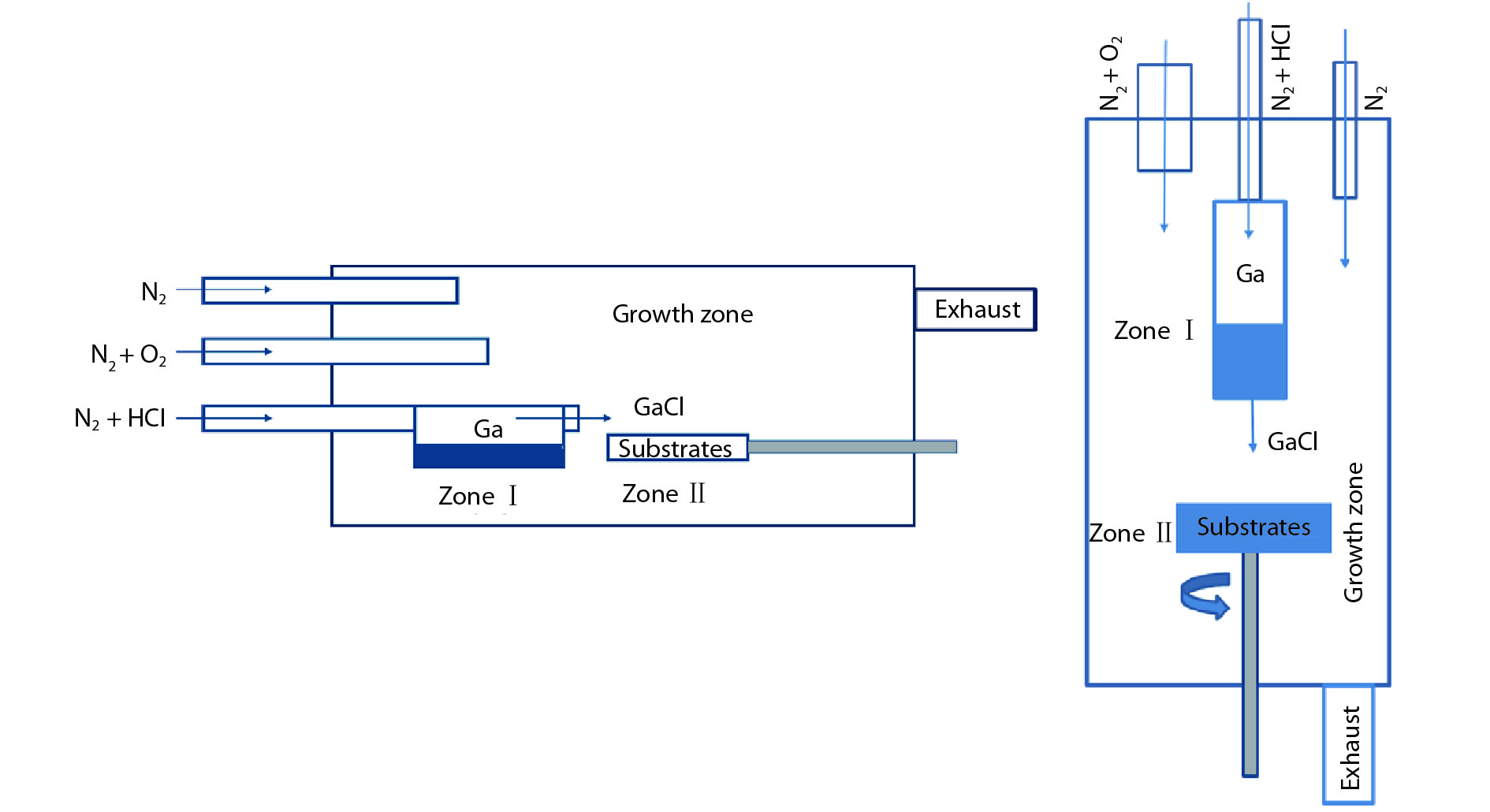
Fig. 1.
(Color online) Schematic diagram of (a) horizontal HVPE and (b) vertical HVPE.
REVIEWS
Xiangqian Xiu, Liying Zhang, Yuewen Li, Zening Xiong, Rong Zhang and Youdou Zheng
Corresponding author: Xiangqian Xiu, Email: xqxiu@nju.edu.cn
Abstract: Halide vapor phase epitaxy (HVPE) is widely used in the semiconductor industry for the growth of Si, GaAs, GaN, etc. HVPE is a non-organic chemical vapor deposition (CVD) technique, characterized by high quality growth of epitaxial layers with fast growth rate, which is versatile for the fabrication of both substrates and devices with wide applications. In this paper, we review the usage of HVPE for the growth and device applications of Ga2O3, with detailed discussions on a variety of technological aspects of HVPE. It is concluded that HVPE is a promising candidate for the epitaxy of large-area Ga2O3 substrates and for the fabrication of high power β-Ga2O3 devices.
Key words: halide vapor phase epitaxy, Ga2O3, Schottky barrier diodes, epitaxy growth
| [1] |
R Roy, V G Hill, E F Osborn, et al. Polymorphism of Ga2O3 and the system Ga2O3–H2O. J Am Chem Soc, 1952,74(3): 719 doi: 10.1021/ja01123a039
|
| [2] |
H H Tippins. Optical absorption and photoconductivity in the band edge of β-Ga2O3. Phys Rev, 1965, 140: A316. doi: 10.1103/PhysRev.140.A316
|
| [3] |
H He, R Orlando, M A Blanco, et al. First-principles study of structural, electronic, and optical properties of Ga2O3 in its monoclinic and hexagonal phases. Phys Rev B, 2006, 74: 195123. doi: 10.1103/PhysRevB.74.195123
|
| [4] |
M Orita, H Ohta, M Hirano, et al. Deep-ultraviolet transparent conductive β-Ga2O3 thin films. Appl Phys Lett, 2000, 77: 4166. doi: 10.1063/1.1330559
|
| [5] |
T Onuma, S Fujioka, T Yamaguchi, et al. Correlation between blue luminescence intensity and resistivity in β-Ga2O3 single crystals. Appl Phys Lett, 2013, 103: 041910. doi: 10.1063/1.4816759
|
| [6] |
T Oshima, T Okuno, N Arai, et al. Vertical solar-blind deep-ultraviolet Schottky photodetectors based on β-Ga2O3 substrates. Appl Phys Express, 2008, 1(1): 011202 doi: 10.1143/APEX.1.011202
|
| [7] |
E G Víllora, K Shimamura, K Kitamura, et al. Epitaxial relationship between wurtzite GaN and β-Ga2O3. Appl Phys Lett, 2007, 90(23): 234102. doi: 10.1063/1.2745645
|
| [8] |
E G Víllora, S Arjoca, K Shimamura, et al. β-Ga2O3 and single-crystal phosphors for high-brightness white LEDs and LDs, and β-Ga2O3 potential for next generation of power devices. Proc SPIE, 2014, 8987: 89871U doi: 10.1117/12.2039305
|
| [9] |
K Sasaki, A Kuramata, T Masui T, et al. Device-quality β-Ga2O3 epitaxial films fabricated by ozone molecular beam epitaxy. Appl Phys Express, 2012, 5(3): 035502. doi: 10.1143/APEX.5.035502
|
| [10] |
M Higashiwaki, K Sasaki, A Kuramata, et al. Gallium oxide (Ga2O3) metal-semiconductor field-effect transistors on single-crystal β-Ga2O3 (010) substrates. Appl Phys Lett, 2012, 100(1): 013504. doi: 10.1063/1.3674287
|
| [11] |
M Higashiwaki, K Sasaki, T Kamimura, et al. Depletion-mode Ga2O3 metal-oxide-semiconductor field-effect transistors on β-Ga2O3 (010) substrates and temperature dependence of their device characteristics. Appl Phys Lett, 2013, 103(12): 123511. doi: 10.1063/1.4821858
|
| [12] |
Z Galazka, K Irmscher, R Uecker, et al. On the bulk β-Ga2O3 single crystals grown by czochralski method. J Cryst Growth, 2014, 404: 184. doi: 10.1016/j.jcrysgro.2014.07.021
|
| [13] |
N Ueda, H Hosono, R Waseda, et al. Anisotropy of electrical and optical properties in β-Ga2O3 single crystals. Appl Phys Lett, 1997, 70: 3561. doi: 10.1063/1.119233
|
| [14] |
E G Villora, K Shimamura, Y Yoshikawa, et al. Large-size β-Ga2O3 single crystals and wafers. J Cryst Growth, 2004, 270: 420. doi: 10.1016/j.jcrysgro.2004.06.027
|
| [15] |
A Kuramata, K Koshi, S Watanabe, et al. High-quality β-Ga2O3 single crystals grown by edge-defined film-fed growth. Jpn J Appl Phys, 2016, 55: 1202A2. doi: 10.7567/JJAP.55.1202A2
|
| [16] |
T Oshima, T Okuno, S Fujita. Ga2O3 thin film growth on c-plane sapphire substrates by molecular beam epitaxy for deep-ultraviolet photodetectors. Jpn J Appl Phys, 2007, 46(11R): 7217. doi: 10.1143/JJAP.46.7217
|
| [17] |
G Wagner, M Baldini, D Gogova, et al. Homoepitaxial growth of β‐Ga2O3 layers by metal‐organic vapor phase epitaxy. Phys Status Solidi A, 2014, 211(1): 27 doi: 10.1002/pssa.201330092
|
| [18] |
K Fujito, S Kubo, H Nagaoka, et al. Bulk GaN crystals grown by HVPE. J Cryst Growth, 2009, 311(10): 3011 doi: 10.1016/j.jcrysgro.2009.01.046
|
| [19] |
R Masuda, T Fujii, N Yoshii, et al. Step-flow growth of homoepitaxial ZnO thin layers by halide vapor phase epitaxy using ZnCl2 and H2O source gases. J Cryst Growth, 2010, 312(16/17): 2324 doi: 10.1016/j.jcrysgro.2010.05.005
|
| [20] |
Y Kumagai, Y Kubota, T Nagashima, et al. Preparation of a freestanding AlN substrate from a thick AlN layer grown by hydride vapor phase epitaxy on a bulk AlN substrate prepared by physical vapor transport. Appl Phys Express, 2012, 5(5): 055504. doi: 10.1143/APEX.5.055504
|
| [21] |
K Nomura, K Goto, R Togashi, et al. Thermodynamic study of β-Ga2O3 growth by halide vapor phase epitaxy. J Cryst Growth, 2014, 405: 19 doi: 10.1016/j.jcrysgro.2014.06.051
|
| [22] |
Y Oshima, E G Vίllora, K Shimamura. Quasi-heteroepitaxial growth of β-Ga2O3 on off-angled sapphire (0001) substrates by halide vapor phase epitaxy. J Cryst Growth, 2015, 410: 53 doi: 10.1016/j.jcrysgro.2014.10.038
|
| [23] |
N Suzuki, S Ohira, M Tanaka, et al. Fabrication and characterization of transparent conductive Sn‐doped β‐Ga2O3 single crystals. Phys Status Solidi C, 2007, 4(7): 2310 doi: 10.1002/(ISSN)1610-1642
|
| [24] |
M Slomski, N Blumenschein, P P Paskov, et al. Anisotropic thermal conductivity of β-Ga2O3 at elevated temperatures: Effect of Sn and Fe dopants. J Appl Phys, 2017, 121(23): 235104. doi: 10.1063/1.4986478
|
| [25] |
T Harwig, G J Wubs, G J Dirksen. Electrical properties of β-Ga2O3 single crystals. Solid State Commun., 1976, 18(9/10): 1223 doi: 10.1016/0038-1098(76)90944-3
|
| [26] |
T Matsumoto, M Aoki, A Kinoshita, et al. Absorption and reflection of vapor grown single crystal platelets of β-Ga2O3. Jpn J Appl Phys, 1974, 13(10): 1578. doi: 10.1143/JJAP.13.1578
|
| [27] |
E G Víllora, K Shimamura, K Kitamura, et al. Rf-plasma-assisted molecular-beam epitaxy of β-Ga2O3. Appl Phys Lett, 2006, 88(3): 031105. doi: 10.1063/1.2164407
|
| [28] |
M Y Tsai, O Bierwagen, M E White, et al. β-Ga2O3 growth by plasma-assisted molecular beam epitaxy. J Vac Sci Technol, 2010, 28(2): 354 doi: 10.1116/1.3294715
|
| [29] |
V Gottschalch, K Mergenthaler, G Wagner, et al. Growth of β‐Ga2O3 on Al2O3 and GaAs using metal‐organic vapor‐phase epitaxy. Phys Stat Solidi (a), 2009, 206(2): 243 doi: 10.1002/pssa.v206:2
|
| [30] |
W Mi, J Ma, Z Zhu, et al. Epitaxial growth of Ga2O3 thin films on MgO (110) substrate by metal–organic chemical vapor deposition. J Cryst Growth, 2012, 354(1): 93 doi: 10.1016/j.jcrysgro.2012.06.022
|
| [31] |
F B Zhang, K Saito, T Tanaka, et al. Structural and optical properties of Ga2O3 films on sapphire substrates by pulsed laser deposition. J Cryst Growth, 2014, 387: 96 doi: 10.1016/j.jcrysgro.2013.11.022
|
| [32] |
Z N Xiong, X Q Xiu, Y W Li, et al. Growth of β-Ga2O3 films on sapphire by HVPE. Chin Phys Lett, 2018, 35: 058101 doi: 10.1088/0256-307X/35/5/058101
|
| [33] |
M Orita, H Hiramatsu, H Ohta, et al. Preparation of highly conductive, deep ultraviolet transparent β-Ga2O3 thin film at low deposition temperatures. Thin Solid Films, 2002, 411(1): 134 doi: 10.1016/S0040-6090(02)00202-X
|
| [34] |
D Shinohara, S Fujita. Heteroepitaxy of corundum-structured α-Ga2O3 thin films on α-Al2O3 substrates by ultrasonic mist chemical vapor deposition. Jpn J Appl Phys, 2008, 47(9R): 7311. doi: 10.1143/JJAP.47.7311
|
| [35] |
T Kawaharamura, G T Dang, M Furuta. Successful growth of conductive highly crystalline Sn-doped α-Ga2O3 thin films by fine-channel mist chemical vapor deposition. Jpn J Appl Phys, 2012, 51(4R): 040207. doi: 10.7567/JJAP.51.040207
|
| [36] |
K Akaiwa, S Fujita. Electrical conductive corundum-structured α-Ga2O3 thin films on sapphire with tin-doping grown by spray-assisted mist chemical vapor deposition. Jpn J Appl Phys, 2012, 51(7R): 070203. doi: 10.7567/JJAP.51.070203
|
| [37] |
S Fujita, K Kaneko. Epitaxial growth of corundum-structured wide band gap III-oxide semiconductor thin films. J Cryst Growth, 2014, 401: 588 doi: 10.1016/j.jcrysgro.2014.02.032
|
| [38] |
Y Oshima, E G Víllora, K Shimamura. Halide vapor phase epitaxy of twin-free α-Ga2O3 on sapphire (0001) substrates. Appl Phys Express, 2015, 8(5): 055501. doi: 10.7567/APEX.8.055501
|
| [39] |
Y Oshima Y, E G Víllora, Y Matsushita, et al. Epitaxial growth of phase-pure ε-Ga2O3 by halide vapor phase epitaxy. J Appl Phys, 2015, 118(8): 085301. doi: 10.1063/1.4929417
|
| [40] |
Y Yao, S Okur, A M Lyle, et al. Growth and characterization of α-, β-, and ϵ-phases of Ga2O3 using MOCVD and HVPE techniques. Mater Res Lett, 2018, 6(5): 268 doi: 10.1080/21663831.2018.1443978
|
| [41] |
M Mohamed, K Irmscher, C Janowitz, et al. Schottky barrier height of Au on the transparent semiconducting oxide β-Ga2O3. Appl Phys Lett, 2012, 101(13): 132106. doi: 10.1063/1.4755770
|
| [42] |
S Oh, G Yang, J Kim. Electrical characteristics of vertical Ni/β-Ga2O3 schottky barrier diodes at high temperatures. ECS J Solid State Sci Technol, 2017, 6(2): Q3022 doi: 10.1149/2.0041702jss
|
| [43] |
J Yang, S Ahn, F Ren, et al. High reverse breakdown voltage Schottky rectifiers without edge termination on Ga2O3. Appl Phys Lett, 2017, 110(19): 192101. doi: 10.1063/1.4983203
|
| [44] |
M Higashiwaki, K Konishi, K Sasaki, et al. Temperature-dependent capacitance–voltage and current–voltage characteristics of Pt/Ga2O3 (001) Schottky barrier diodes fabricated on n––Ga2O3 drift layers grown by halide vapor phase epitaxy. Appl Phys Lett, 2016, 108(13): 133503. doi: 10.1063/1.4945267
|
| [45] |
H Murakami, K Nomura, K Goto, et al. Homoepitaxial growth of β-Ga2O3 layers by halide vapor phase epitaxy. Appl Phys Express, 2014, 8(1): 015503. doi: 10.7567/APEX.8.015503
|
| [46] |
Z Z Hu, H Zhou, Q Feng, et al. Field-plated lateral β- Ga2O3 Schottky barrier diode with high reverse blocking voltage of more than 3 kV and high DC power figure-of-merit of 500 MW/cm2. IEEE Electron Device Lett, 2018, 39 (10): 1564 doi: 10.1109/LED.2018.2868444
|
| [47] |
M Higashiwaki, K Sasaki, H Murakami, et al. Recent progress in Ga2O3 power devices. Semicond Sci Technol, 2016, 31(3): 034001. doi: 10.1088/0268-1242/31/3/034001
|
| [48] |
K Konishi, K Goto, H Murakami, et al. 1-kV vertical Ga2O3 field-plated Schottky barrier diodes. Appl Phys Lett, 2017, 110(10): 103506. doi: 10.1063/1.4977857
|
| [49] |
K Shimamura, E G Víllora, K Domen, et al. Epitaxial growth of GaN on (100) β-Ga2O3 substrates by metalorganic vapor phase epitaxy. Jpn J Appl Phys, 2004, 44(1L): L7. doi: 10.1143/JJAP.44.L7
|
| [50] |
E G Víllora, K Shimamura, K Aoki, et al. Molecular beam epitaxy of c-plane wurtzite GaN on nitridized a-plane β-Ga2O3. Thin Solid Films, 2006, 500(1/2): 209 doi: 10.1016/j.tsf.2005.10.080
|
| [51] |
Z L Xie, R Zhang, C T Xia, et al. Demonstration of GaN/InGaN light emitting diodes on (100) beta-Ga2O3 substrates by metalorganic chemical vapour deposition. Chin Phys Lett, 2008, 25: 2185 doi: 10.1088/0256-307X/25/6/071
|
| [52] |
I A Ajia, Y Yamashita, K Lorenz, et al. GaN/AlGaN multiple quantum wells grown on transparent and conductive (-201)-oriented β-Ga2O3 substrate for UV vertical light emitting devices. Appl Phys Lett, 2018, 113(8): 082102. doi: 10.1063/1.5025178
|
| [53] |
V M Krymov, S I Stepanov, N K Zhumashev, et al. GaN growth on β-Ga2O3 substrates by HVPE. Mater Phys Mech, 2015, 22: 59
|
| [54] |
S Ito, K Takeda, K Nagata, et al. Growth of GaN and AlGaN on (100) β‐Ga2O3 substrates. Phys. Stat. Solidi c, 2012, 9(3/4): 519 doi: 10.1002/pssc.201100499
|
| [55] |
H J Lee, T I Shin, D H Yoon. Influence of NH3 gas for GaN epilayer on β-Ga2O3 substrate by nitridation. Surf Coat.Tech, 2008, 202(22/23): 5497 doi: 10.1016/j.surfcoat.2008.06.103
|
| [56] |
K Kachel, M Korytov, D Gogova, et al. A new approach to free-standing GaN using β-Ga2O3 as a substrate. CrystEngComm, 2012, 14(24): 8536 doi: 10.1039/c2ce25976a
|
| [57] |
V I Nikolaev, A I Pechnikov, V N Maslov, et al. GaN growth on β-Ga2O3 substrates by HVPE. Mater Phys Mechan, 2015, 22:59 doi: 10.4028/www.scientific.net/KEM.674.302
|
| [58] |
Y W Li, X Q Xiu, Z N Xiong, et al. Single crystal GaN layer converted from β-Ga2O3 films and its application for free-Standing GaN. CrystEngComm, 2019, DOI: 10.1039/C8CE01336E
|


Article views: 5705 Times PDF downloads: 359 Times Cited by: 0 Times
Received: 27 September 2018 Revised: 04 December 2018 Online: Accepted Manuscript: 03 January 2019Uncorrected proof: 04 January 2019Published: 07 January 2019
| Citation: |
Xiangqian Xiu, Liying Zhang, Yuewen Li, Zening Xiong, Rong Zhang, Youdou Zheng. Application of halide vapor phase epitaxy for the growth of ultra-wide band gap Ga2O3[J]. Journal of Semiconductors, 2019, 40(1): 011805. doi: 10.1088/1674-4926/40/1/011805
****
X Q Xiu, L Y Zhang, Y W Li, Z N Xiong, R Zhang, Y D Zheng, Application of halide vapor phase epitaxy for the growth of ultra-wide band gap Ga2O3[J]. J. Semicond., 2019, 40(1): 011805. doi: 10.1088/1674-4926/40/1/011805.

|
| [1] |
R Roy, V G Hill, E F Osborn, et al. Polymorphism of Ga2O3 and the system Ga2O3–H2O. J Am Chem Soc, 1952,74(3): 719 doi: 10.1021/ja01123a039
|
| [2] |
H H Tippins. Optical absorption and photoconductivity in the band edge of β-Ga2O3. Phys Rev, 1965, 140: A316. doi: 10.1103/PhysRev.140.A316
|
| [3] |
H He, R Orlando, M A Blanco, et al. First-principles study of structural, electronic, and optical properties of Ga2O3 in its monoclinic and hexagonal phases. Phys Rev B, 2006, 74: 195123. doi: 10.1103/PhysRevB.74.195123
|
| [4] |
M Orita, H Ohta, M Hirano, et al. Deep-ultraviolet transparent conductive β-Ga2O3 thin films. Appl Phys Lett, 2000, 77: 4166. doi: 10.1063/1.1330559
|
| [5] |
T Onuma, S Fujioka, T Yamaguchi, et al. Correlation between blue luminescence intensity and resistivity in β-Ga2O3 single crystals. Appl Phys Lett, 2013, 103: 041910. doi: 10.1063/1.4816759
|
| [6] |
T Oshima, T Okuno, N Arai, et al. Vertical solar-blind deep-ultraviolet Schottky photodetectors based on β-Ga2O3 substrates. Appl Phys Express, 2008, 1(1): 011202 doi: 10.1143/APEX.1.011202
|
| [7] |
E G Víllora, K Shimamura, K Kitamura, et al. Epitaxial relationship between wurtzite GaN and β-Ga2O3. Appl Phys Lett, 2007, 90(23): 234102. doi: 10.1063/1.2745645
|
| [8] |
E G Víllora, S Arjoca, K Shimamura, et al. β-Ga2O3 and single-crystal phosphors for high-brightness white LEDs and LDs, and β-Ga2O3 potential for next generation of power devices. Proc SPIE, 2014, 8987: 89871U doi: 10.1117/12.2039305
|
| [9] |
K Sasaki, A Kuramata, T Masui T, et al. Device-quality β-Ga2O3 epitaxial films fabricated by ozone molecular beam epitaxy. Appl Phys Express, 2012, 5(3): 035502. doi: 10.1143/APEX.5.035502
|
| [10] |
M Higashiwaki, K Sasaki, A Kuramata, et al. Gallium oxide (Ga2O3) metal-semiconductor field-effect transistors on single-crystal β-Ga2O3 (010) substrates. Appl Phys Lett, 2012, 100(1): 013504. doi: 10.1063/1.3674287
|
| [11] |
M Higashiwaki, K Sasaki, T Kamimura, et al. Depletion-mode Ga2O3 metal-oxide-semiconductor field-effect transistors on β-Ga2O3 (010) substrates and temperature dependence of their device characteristics. Appl Phys Lett, 2013, 103(12): 123511. doi: 10.1063/1.4821858
|
| [12] |
Z Galazka, K Irmscher, R Uecker, et al. On the bulk β-Ga2O3 single crystals grown by czochralski method. J Cryst Growth, 2014, 404: 184. doi: 10.1016/j.jcrysgro.2014.07.021
|
| [13] |
N Ueda, H Hosono, R Waseda, et al. Anisotropy of electrical and optical properties in β-Ga2O3 single crystals. Appl Phys Lett, 1997, 70: 3561. doi: 10.1063/1.119233
|
| [14] |
E G Villora, K Shimamura, Y Yoshikawa, et al. Large-size β-Ga2O3 single crystals and wafers. J Cryst Growth, 2004, 270: 420. doi: 10.1016/j.jcrysgro.2004.06.027
|
| [15] |
A Kuramata, K Koshi, S Watanabe, et al. High-quality β-Ga2O3 single crystals grown by edge-defined film-fed growth. Jpn J Appl Phys, 2016, 55: 1202A2. doi: 10.7567/JJAP.55.1202A2
|
| [16] |
T Oshima, T Okuno, S Fujita. Ga2O3 thin film growth on c-plane sapphire substrates by molecular beam epitaxy for deep-ultraviolet photodetectors. Jpn J Appl Phys, 2007, 46(11R): 7217. doi: 10.1143/JJAP.46.7217
|
| [17] |
G Wagner, M Baldini, D Gogova, et al. Homoepitaxial growth of β‐Ga2O3 layers by metal‐organic vapor phase epitaxy. Phys Status Solidi A, 2014, 211(1): 27 doi: 10.1002/pssa.201330092
|
| [18] |
K Fujito, S Kubo, H Nagaoka, et al. Bulk GaN crystals grown by HVPE. J Cryst Growth, 2009, 311(10): 3011 doi: 10.1016/j.jcrysgro.2009.01.046
|
| [19] |
R Masuda, T Fujii, N Yoshii, et al. Step-flow growth of homoepitaxial ZnO thin layers by halide vapor phase epitaxy using ZnCl2 and H2O source gases. J Cryst Growth, 2010, 312(16/17): 2324 doi: 10.1016/j.jcrysgro.2010.05.005
|
| [20] |
Y Kumagai, Y Kubota, T Nagashima, et al. Preparation of a freestanding AlN substrate from a thick AlN layer grown by hydride vapor phase epitaxy on a bulk AlN substrate prepared by physical vapor transport. Appl Phys Express, 2012, 5(5): 055504. doi: 10.1143/APEX.5.055504
|
| [21] |
K Nomura, K Goto, R Togashi, et al. Thermodynamic study of β-Ga2O3 growth by halide vapor phase epitaxy. J Cryst Growth, 2014, 405: 19 doi: 10.1016/j.jcrysgro.2014.06.051
|
| [22] |
Y Oshima, E G Vίllora, K Shimamura. Quasi-heteroepitaxial growth of β-Ga2O3 on off-angled sapphire (0001) substrates by halide vapor phase epitaxy. J Cryst Growth, 2015, 410: 53 doi: 10.1016/j.jcrysgro.2014.10.038
|
| [23] |
N Suzuki, S Ohira, M Tanaka, et al. Fabrication and characterization of transparent conductive Sn‐doped β‐Ga2O3 single crystals. Phys Status Solidi C, 2007, 4(7): 2310 doi: 10.1002/(ISSN)1610-1642
|
| [24] |
M Slomski, N Blumenschein, P P Paskov, et al. Anisotropic thermal conductivity of β-Ga2O3 at elevated temperatures: Effect of Sn and Fe dopants. J Appl Phys, 2017, 121(23): 235104. doi: 10.1063/1.4986478
|
| [25] |
T Harwig, G J Wubs, G J Dirksen. Electrical properties of β-Ga2O3 single crystals. Solid State Commun., 1976, 18(9/10): 1223 doi: 10.1016/0038-1098(76)90944-3
|
| [26] |
T Matsumoto, M Aoki, A Kinoshita, et al. Absorption and reflection of vapor grown single crystal platelets of β-Ga2O3. Jpn J Appl Phys, 1974, 13(10): 1578. doi: 10.1143/JJAP.13.1578
|
| [27] |
E G Víllora, K Shimamura, K Kitamura, et al. Rf-plasma-assisted molecular-beam epitaxy of β-Ga2O3. Appl Phys Lett, 2006, 88(3): 031105. doi: 10.1063/1.2164407
|
| [28] |
M Y Tsai, O Bierwagen, M E White, et al. β-Ga2O3 growth by plasma-assisted molecular beam epitaxy. J Vac Sci Technol, 2010, 28(2): 354 doi: 10.1116/1.3294715
|
| [29] |
V Gottschalch, K Mergenthaler, G Wagner, et al. Growth of β‐Ga2O3 on Al2O3 and GaAs using metal‐organic vapor‐phase epitaxy. Phys Stat Solidi (a), 2009, 206(2): 243 doi: 10.1002/pssa.v206:2
|
| [30] |
W Mi, J Ma, Z Zhu, et al. Epitaxial growth of Ga2O3 thin films on MgO (110) substrate by metal–organic chemical vapor deposition. J Cryst Growth, 2012, 354(1): 93 doi: 10.1016/j.jcrysgro.2012.06.022
|
| [31] |
F B Zhang, K Saito, T Tanaka, et al. Structural and optical properties of Ga2O3 films on sapphire substrates by pulsed laser deposition. J Cryst Growth, 2014, 387: 96 doi: 10.1016/j.jcrysgro.2013.11.022
|
| [32] |
Z N Xiong, X Q Xiu, Y W Li, et al. Growth of β-Ga2O3 films on sapphire by HVPE. Chin Phys Lett, 2018, 35: 058101 doi: 10.1088/0256-307X/35/5/058101
|
| [33] |
M Orita, H Hiramatsu, H Ohta, et al. Preparation of highly conductive, deep ultraviolet transparent β-Ga2O3 thin film at low deposition temperatures. Thin Solid Films, 2002, 411(1): 134 doi: 10.1016/S0040-6090(02)00202-X
|
| [34] |
D Shinohara, S Fujita. Heteroepitaxy of corundum-structured α-Ga2O3 thin films on α-Al2O3 substrates by ultrasonic mist chemical vapor deposition. Jpn J Appl Phys, 2008, 47(9R): 7311. doi: 10.1143/JJAP.47.7311
|
| [35] |
T Kawaharamura, G T Dang, M Furuta. Successful growth of conductive highly crystalline Sn-doped α-Ga2O3 thin films by fine-channel mist chemical vapor deposition. Jpn J Appl Phys, 2012, 51(4R): 040207. doi: 10.7567/JJAP.51.040207
|
| [36] |
K Akaiwa, S Fujita. Electrical conductive corundum-structured α-Ga2O3 thin films on sapphire with tin-doping grown by spray-assisted mist chemical vapor deposition. Jpn J Appl Phys, 2012, 51(7R): 070203. doi: 10.7567/JJAP.51.070203
|
| [37] |
S Fujita, K Kaneko. Epitaxial growth of corundum-structured wide band gap III-oxide semiconductor thin films. J Cryst Growth, 2014, 401: 588 doi: 10.1016/j.jcrysgro.2014.02.032
|
| [38] |
Y Oshima, E G Víllora, K Shimamura. Halide vapor phase epitaxy of twin-free α-Ga2O3 on sapphire (0001) substrates. Appl Phys Express, 2015, 8(5): 055501. doi: 10.7567/APEX.8.055501
|
| [39] |
Y Oshima Y, E G Víllora, Y Matsushita, et al. Epitaxial growth of phase-pure ε-Ga2O3 by halide vapor phase epitaxy. J Appl Phys, 2015, 118(8): 085301. doi: 10.1063/1.4929417
|
| [40] |
Y Yao, S Okur, A M Lyle, et al. Growth and characterization of α-, β-, and ϵ-phases of Ga2O3 using MOCVD and HVPE techniques. Mater Res Lett, 2018, 6(5): 268 doi: 10.1080/21663831.2018.1443978
|
| [41] |
M Mohamed, K Irmscher, C Janowitz, et al. Schottky barrier height of Au on the transparent semiconducting oxide β-Ga2O3. Appl Phys Lett, 2012, 101(13): 132106. doi: 10.1063/1.4755770
|
| [42] |
S Oh, G Yang, J Kim. Electrical characteristics of vertical Ni/β-Ga2O3 schottky barrier diodes at high temperatures. ECS J Solid State Sci Technol, 2017, 6(2): Q3022 doi: 10.1149/2.0041702jss
|
| [43] |
J Yang, S Ahn, F Ren, et al. High reverse breakdown voltage Schottky rectifiers without edge termination on Ga2O3. Appl Phys Lett, 2017, 110(19): 192101. doi: 10.1063/1.4983203
|
| [44] |
M Higashiwaki, K Konishi, K Sasaki, et al. Temperature-dependent capacitance–voltage and current–voltage characteristics of Pt/Ga2O3 (001) Schottky barrier diodes fabricated on n––Ga2O3 drift layers grown by halide vapor phase epitaxy. Appl Phys Lett, 2016, 108(13): 133503. doi: 10.1063/1.4945267
|
| [45] |
H Murakami, K Nomura, K Goto, et al. Homoepitaxial growth of β-Ga2O3 layers by halide vapor phase epitaxy. Appl Phys Express, 2014, 8(1): 015503. doi: 10.7567/APEX.8.015503
|
| [46] |
Z Z Hu, H Zhou, Q Feng, et al. Field-plated lateral β- Ga2O3 Schottky barrier diode with high reverse blocking voltage of more than 3 kV and high DC power figure-of-merit of 500 MW/cm2. IEEE Electron Device Lett, 2018, 39 (10): 1564 doi: 10.1109/LED.2018.2868444
|
| [47] |
M Higashiwaki, K Sasaki, H Murakami, et al. Recent progress in Ga2O3 power devices. Semicond Sci Technol, 2016, 31(3): 034001. doi: 10.1088/0268-1242/31/3/034001
|
| [48] |
K Konishi, K Goto, H Murakami, et al. 1-kV vertical Ga2O3 field-plated Schottky barrier diodes. Appl Phys Lett, 2017, 110(10): 103506. doi: 10.1063/1.4977857
|
| [49] |
K Shimamura, E G Víllora, K Domen, et al. Epitaxial growth of GaN on (100) β-Ga2O3 substrates by metalorganic vapor phase epitaxy. Jpn J Appl Phys, 2004, 44(1L): L7. doi: 10.1143/JJAP.44.L7
|
| [50] |
E G Víllora, K Shimamura, K Aoki, et al. Molecular beam epitaxy of c-plane wurtzite GaN on nitridized a-plane β-Ga2O3. Thin Solid Films, 2006, 500(1/2): 209 doi: 10.1016/j.tsf.2005.10.080
|
| [51] |
Z L Xie, R Zhang, C T Xia, et al. Demonstration of GaN/InGaN light emitting diodes on (100) beta-Ga2O3 substrates by metalorganic chemical vapour deposition. Chin Phys Lett, 2008, 25: 2185 doi: 10.1088/0256-307X/25/6/071
|
| [52] |
I A Ajia, Y Yamashita, K Lorenz, et al. GaN/AlGaN multiple quantum wells grown on transparent and conductive (-201)-oriented β-Ga2O3 substrate for UV vertical light emitting devices. Appl Phys Lett, 2018, 113(8): 082102. doi: 10.1063/1.5025178
|
| [53] |
V M Krymov, S I Stepanov, N K Zhumashev, et al. GaN growth on β-Ga2O3 substrates by HVPE. Mater Phys Mech, 2015, 22: 59
|
| [54] |
S Ito, K Takeda, K Nagata, et al. Growth of GaN and AlGaN on (100) β‐Ga2O3 substrates. Phys. Stat. Solidi c, 2012, 9(3/4): 519 doi: 10.1002/pssc.201100499
|
| [55] |
H J Lee, T I Shin, D H Yoon. Influence of NH3 gas for GaN epilayer on β-Ga2O3 substrate by nitridation. Surf Coat.Tech, 2008, 202(22/23): 5497 doi: 10.1016/j.surfcoat.2008.06.103
|
| [56] |
K Kachel, M Korytov, D Gogova, et al. A new approach to free-standing GaN using β-Ga2O3 as a substrate. CrystEngComm, 2012, 14(24): 8536 doi: 10.1039/c2ce25976a
|
| [57] |
V I Nikolaev, A I Pechnikov, V N Maslov, et al. GaN growth on β-Ga2O3 substrates by HVPE. Mater Phys Mechan, 2015, 22:59 doi: 10.4028/www.scientific.net/KEM.674.302
|
| [58] |
Y W Li, X Q Xiu, Z N Xiong, et al. Single crystal GaN layer converted from β-Ga2O3 films and its application for free-Standing GaN. CrystEngComm, 2019, DOI: 10.1039/C8CE01336E
|

 WeChat ID
Journal of Semiconductors © 2017 All Rights Reserved 京ICP备05085259号-2

 DownLoad: