J. Semicond. > 2019, Volume 40 > Issue 9 > 092002

ARTICLES

A gate-free MoS2 phototransistor assisted by ferroelectrics

Shuaiqin Wu1, 2, Guangjian Wu1, Xudong Wang1, Yan Chen1, Tie Lin1, 2, Hong Shen1, 2, Weida Hu1, 2, , Xiangjian Meng1, 2, Jianlu Wang1, 2, and Junhao Chu1, 2

+ Author Affiliations

 Corresponding author: Weida Hu: wdhu@mail.sitp.ac.cn; Jianlu Wang: jlwang@mail.sitp.ac.cn

DOI: 10.1088/1674-4926/40/9/092002

PDF

Turn off MathJax

Abstract: 
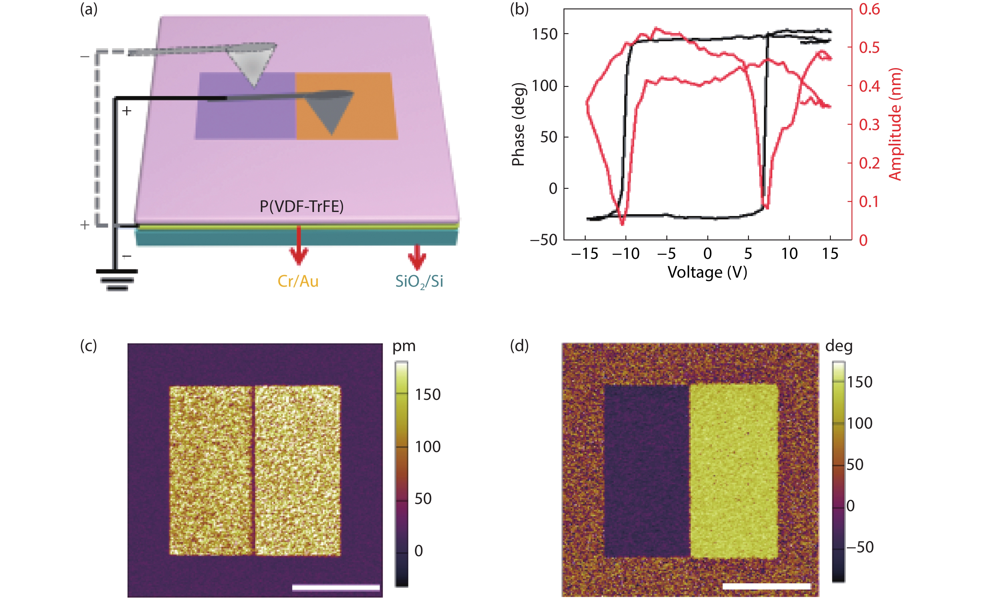
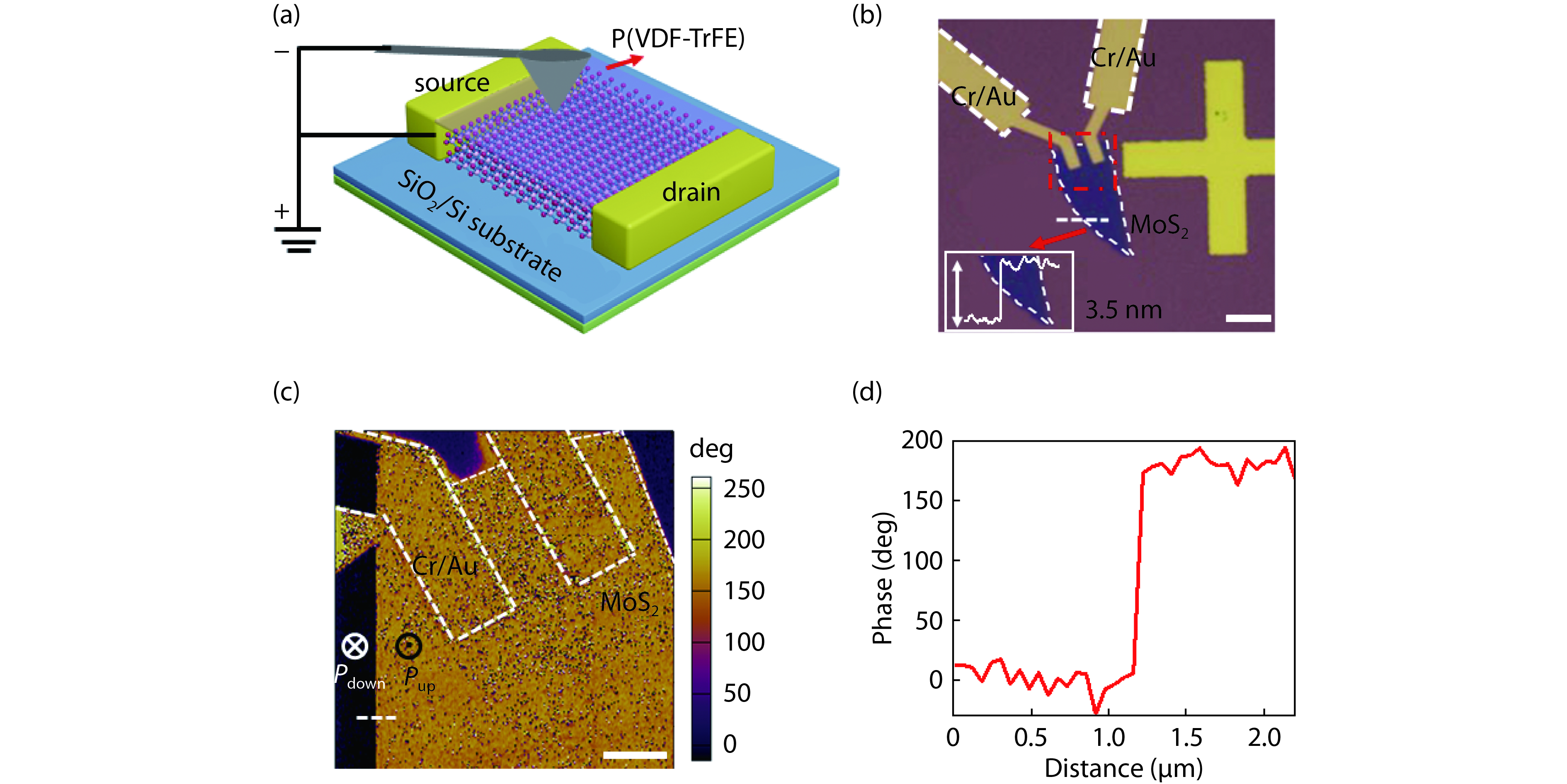
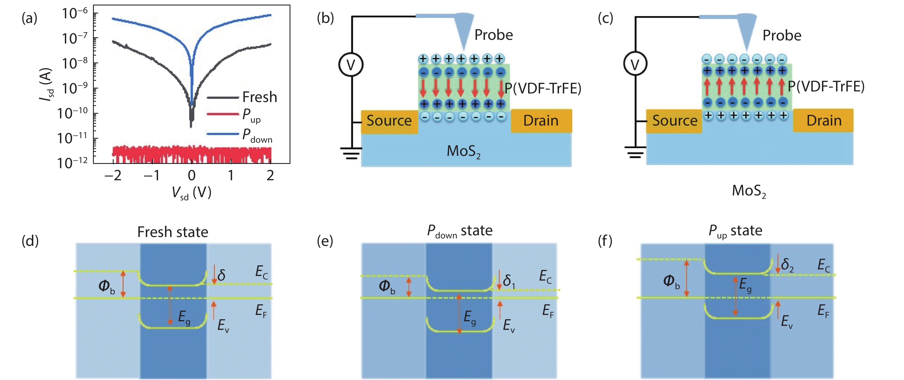
During the past decades, transition metal dichalcogenides (TMDs) have received special focus for their unique properties in photoelectric detection. As one important member of TMDs, MoS2 has been made into photodetector purely or combined with other materials, such as graphene, ionic liquid, and ferroelectric materials. Here, we report a gate-free MoS2 phototransistor combined with organic ferroelectric material poly(vinylidene fluoride-trifluoroethylene) (P(VDF-TrFE)). In this device, the remnant polarization field in P(VDF-TrFE) is obtained from the piezoelectric force microscope (PFM) probe with a positive or negative bias, which can turn the dipoles from disorder to be the same direction. Then, the MoS2 channel can be maintained at an accumulated state with downward polarization field modulation and a depleted state with upward polarization field modulation. Moreover, the P(VDF-TrFE) segregates MoS2 from oxygen and water molecules around surroundings, which enables a cleaner surface state. As a photodetector, an ultra-low dark current of 10–11 A, on/off ration of more than 104 and a fast photoresponse time of 120 μs are achieved. This work provides a new method to make high-performance phototransistors assisted by the ferroelectric domain which can operate without a gate electrode and demonstrates great potential for ultra-low power consumption applications.

Key words: TMDsMoS2 phototransistorP(VDF-TrFE)PFMultra-low power consumption


[1]
Wang J. A novel spin-FET based on 2D antiferromagnet. J Semicond, 2019, 40(2), 020401 doi: 10.1088/1674-4926/40/2/020401
[2]
Jiang W, Wang X, Chen Y, et al. Large-area high quality PtSe2 thin film with versatile polarity. InfoMat, 2019, 1, 260 doi: 10.1002/inf2.12013
[3]
Wu G, Wang X, Chen Y, et al. Ultrahigh photoresponsivity MoS2 photodetector with tunable photocurrent generation mechanism. Nanotechnology, 2018, 29(48), 485204 doi: 10.1088/1361-6528/aae17e
[4]
Liu L, Wang X, Han L, et al. Electrical characterization of MoS2 field-effect transistors with different dielectric polymer gate. AIP Adv, 2017, 7(6), 065121 doi: 10.1063/1.4991843
[5]
Xue S, Zhao X L, Wang J L, et al. Preparation of La0.67Ca0.23- Sr0.1MnO3 thin films with interesting electrical and magnetic properties via pulsed-laser deposition. Sci Chin Phys, Mechan, Astron, 2017, 60(2), 027521 doi: 10.1007/s11433-016-0368-6
[6]
Wang J, Fang H, Wang X, et al. Recent progress on localized field enhanced two-dimensional material photodetectors from ultraviolet-visible to infrared. Small, 2017, 13(35), 1700894 doi: 10.1002/smll.201700894
[7]
Son Y W, Cohen M L, Louie S G. Energy gaps in graphene nanoribbons. Phys Rev Lett, 2006, 97(21), 216803 doi: 10.1103/PhysRevLett.97.216803
[8]
Meyer J C, Geim A K, Katsnelson M I, et al. The structure of suspended graphene sheets. Nature, 2007, 446(7131), 60 doi: 10.1038/nature05545
[9]
Peelaers H, Van de Walle C G. Effects of strain on band structure and effective masses in MoS2. Phys Rev B, 2012, 86(24), 241401 doi: 10.1103/PhysRevB.86.241401
[10]
Kang D H, Kim M S, Shim J, et al. High-performance transition metal dichalcogenide photodetectors enhanced by self-assembled monolayer doping. Adv Funct Mater, 2015, 25(27), 4219 doi: 10.1002/adfm.201501170
[11]
Wang L, Jie J, Shao Z, et al. MoS2/Si heterojunction with vertically standing layered structure for ultrafast, high-detectivity, self-driven visible-near infrared photodetectors. Adv Funct Maters, 2015, 25(19), 2910 doi: 10.1002/adfm.201500216
[12]
Jariwala D, Sangwan V K, Wu C C, et al. Gate-tunable carbon nanotube-MoS2 heterojunction pn diode. Proc Nat Acad Sci, 2013, 110(45), 18076 doi: 10.1073/pnas.1317226110
[13]
Novoselov K S, Geim A K, Morozov S V, et al. Electric field effect in atomically thin carbon films. Science, 2004, 306(5696), 666 doi: 10.1126/science.1102896
[14]
Addou R, Colombo L, Wallace R M. Surface defects on natural MoS2. ACS Appl Mater Interfaces, 2015, 7(22), 11921 doi: 10.1021/acsami.5b01778
[15]
Di Bartolomeo A, Genovese L, Giubileo F, et al. Hysteresis in the transfer characteristics of MoS2 transistors. 2D Mater, 2017, 5(1), 015014 doi: 10.1088/2053-1583/aa91a7
[16]
Kwon J, Hong Y K, Han G, et al. Giant photoamplification in indirect-bandgap multilayer MoS2 phototransistors with local bottom-gate structures. Adv Mater, 2015, 27(13), 2224 doi: 10.1002/adma.201404367
[17]
Zhang W, Huang J K, Chen C H, et al. High-gain phototransistors based on a CVD MoS2 monolayer. Adv Mater, 2013, 25(25), 3456 doi: 10.1002/adma.201301244
[18]
Wu C L, Chen J W. Chen C H, et al. A gate-free monolayer WSe2 pn diode. APS Meeting Abstracts, 2018
[19]
Baeumer C, Saldana-Greco D, Martirez J M P, et al. Ferroelectrically driven spatial carrier density modulation in graphene. Nat Commun, 2015, 6, 6136 doi: 10.1038/ncomms7136
[20]
Yin C, Wang X, Chen Y, et al. A ferroelectric relaxor polymer-enhanced p-type WSe2 transistor. Nanoscale, 2018, 10(4), 1727 doi: 10.1039/C7NR08034D
[21]
Tian B B, Wang J L, Fusil S, et al. Tunnel electroresistance through organic ferroelectrics. Nat Commun, 2016, 7, 11502 doi: 10.1038/ncomms11502
[22]
Wang X, Wang P, Wang J, et al. Ultrasensitive and broadband MoS2 photodetector driven by ferroelectrics. Adv Mater, 2015, 27(42), 6575 doi: 10.1002/adma.201503340
[23]
Kufer D, Konstantatos G. Highly sensitive, encapsulated MoS2 photodetector with gate controllable gain and speed. Nano Lett, 2015, 15(11), 7307 doi: 10.1021/acs.nanolett.5b02559
[24]
Lee H S, Min S W, Park M K, et al. MoS2 nanosheets for top-gate nonvolatile memory transistor channel. Small, 2012, 8(20), 3111 doi: 10.1002/smll.201200752
[25]
Zhang E, Wang W, Zhang C, et al. Tunable charge-trap memory based on few-layer MoS2. ACS Nano, 2014, 9(1), 612 doi: 10.1021/nn5059419
[26]
Zhao D, Katsouras I, Asadi K, et al. Switching dynamics in ferroelectric P (VDF-TrFE) thin films. Phys Rev B, 2015, 92(21), 214115 doi: 10.1103/PhysRevB.92.214115
[27]
Furchi M M, Polyushkin D K, Pospischil A, et al. Mechanisms of photoconductivity in atomically thin MoS2. Nano Lett, 2014, 14(11), 6165 doi: 10.1021/nl502339q
[28]
Lee H S, Min S W, Chang Y G, et al. MoS2 nanosheet phototransistors with thickness-modulated optical energy gap. Nano Lett, 2012, 12(7), 3695 doi: 10.1021/nl301485q
[29]
Li H, Wu J, Yin Z, et al. Preparation and applications of mechanically exfoliated single-layer and multilayer MoS2 and WSe2 nanosheets. Acc Chem Res, 2014, 47(4), 1067 doi: 10.1021/ar4002312
[30]
Gruverman A, Kalinin S V. Piezoresponse force microscopy and recent advances in nanoscale studies of ferroelectrics. J Mater Sci, 2006, 41(1), 107 doi: 10.1007/s10853-005-5946-0
[31]
Chen X, Wu Z, Xu S, et al. Probing the electron states and metal-insulator transition mechanisms in molybdenum disulphide vertical heterostructures. Nat Commun, 2015, 6, 6088 doi: 10.1038/ncomms7088
[32]
Santos E J G, Kaxiras E. Electrically driven tuning of the dielectric constant in MoS2 layers. ACS Nano, 2013, 7(12), 10741 doi: 10.1021/nn403738b
[33]
Xie Y, Zhang B, Wang S, et al. Ultrabroadband MoS2 photodetector with spectral response from 445 to 2717 nm. Adv Mater, 2017, 29(17), 1605972 doi: 10.1002/adma.201605972
[34]
Lopez-Sanchez O, Lembke D, Kayci M, et al. Ultrasensitive photodetectors based on monolayer MoS2. Nat Nanotechnol, 2013, 8(7), 497 doi: 10.1038/nnano.2013.100
[35]
McCreary K M, Hanbicki A T, Robinson J T, et al. Large-area synthesis of continuous and uniform MoS2 monolayer films on graphene. Adv Funct Mater, 2014, 24(41), 6449 doi: 10.1002/adfm.201401511
[36]
Long M, Wang P, Fang H, et al. Progress, challenges, and opportunities for 2D material based photodetectors. Adv Funct Mater, 2019, 29(19), 1803807 doi: 10.1002/adfm.201803807
[37]
Yin L, Wang Z, Wang F, et al. Ferroelectric-induced carrier modulation for ambipolar transition metal dichalcogenide transistors. Appl Phys Lett, 2017, 110(12) doi: 10.1063/1.4979088
[38]
Choi W, Cho M Y, Konar A, et al. High-detectivity multilayer MoS2 phototransistors with spectral response from ultraviolet to infrared. Adv Mater, 2012, 24(43), 5832 doi: 10.1002/adma.201201909
Fig. 1.  (Color online) Ferroelectric polarization switching by PFM for 50 nm-thick P(VDF-TrFE) film. (a) Schematic of the operation for P(VDF-TrFE) polarization switching with PFM probe appling a positive or negative voltage. (b) The PFM amplitude (red) and phase (black) hysteresis loops during the switching process, scale bar is 10 μm. (c) Amplitude signal and (d) phase signal of the P(VDF-TrFE) film after writing half-to-half rectangle patterns with reversed DC bias, scale bar is 10 μm.

Fig. 2.  (Color online) Structure illustration of the gate-free MoS2 photodetector. (a) A 3D schematic of the device structure. (b) The optical image of the device, which includes a 3.5 nm MoS2 and Cr/Au source and drain electrodes covered by 50 nm-thick P(VDF-TrFE) film, scale bar is 10 μm. (c) The PFM phase image of the device (red square part in (b)), two polarization states of Pdown and Pup represent the opposite direction of the electric dipole moment in different parts (orange and black), scale bar is 3 μm. (d) Phase profile extracted along the white dashed line in (c), which demonstrated that the MoS2 in the channel has a 180° phase difference with the other part.

Fig. 3.  (Color online) Electrical characteristics of the device with three different polarization states of P(VDF-TrFE). (a) The IsdVsd characteristics of the device with three different polarization states of P(VDF-TrFE). These three polarization states are fresh (without polarization), Pup (upward polarization) and Pdown state (downward polarization). (b) Sectional view of the device for illustrating the distribution of electron and hole under downward and (c) upward polarization state. (d–f) The energy band diagrams of the device with three polarization states at Vsd = 0 V. Φb is the Schottky barrier height, Eg is the energy gap of MoS2, δ is the barrier height from conduction band to Fermi level.

Fig. 4.  (Color online) Optoelectronic properties of the device. (a) IsdVsd curves of the device under dark and different power of incident light (520 nm). (b) photocurrent switching characteristic of the device with 520 nm laser illumination. The light power is 6.56 μW and Vsd = 1 V. (c) The photocurrent map of the device recorded at Pup state and Vsd = 1 V, the incident light power is 0.28 μW, scale bar = 3 μm. (d, e) The photocurrent rise and fall time extracted from a photocurrent switching cycle. (f) The photoresponse characteristic of the device under incident light with the different wavelengths but the same power.

Table 1.   Photoresponse speed comparation between our device and other MoS2-based photodetectors.

DescriptionResponse time (s)Wavelength (nm)Gate voltage /BiasRef.
MoS2–SiO2–Si back gate2532Vg = 100 V, Vsd = 5 V[27]
MoS2–SiO2–Si back gate (CVD)3532Vg = 40 V, Vsd = 1 V[17]
MoS2–Al2O3–ITO top gate0.3580Vg = –9 V, Vsd = 1 V[28]
MoS2–SiO2–Si back gate0.05488Vg = 50 V, Vsd = 1 V[29]
MoS2–P(VDF-TrFE)1.2 × 10–4520Vg = 0 V, Vsd = 1 VThis work
DownLoad: CSV
[1]
Wang J. A novel spin-FET based on 2D antiferromagnet. J Semicond, 2019, 40(2), 020401 doi: 10.1088/1674-4926/40/2/020401
[2]
Jiang W, Wang X, Chen Y, et al. Large-area high quality PtSe2 thin film with versatile polarity. InfoMat, 2019, 1, 260 doi: 10.1002/inf2.12013
[3]
Wu G, Wang X, Chen Y, et al. Ultrahigh photoresponsivity MoS2 photodetector with tunable photocurrent generation mechanism. Nanotechnology, 2018, 29(48), 485204 doi: 10.1088/1361-6528/aae17e
[4]
Liu L, Wang X, Han L, et al. Electrical characterization of MoS2 field-effect transistors with different dielectric polymer gate. AIP Adv, 2017, 7(6), 065121 doi: 10.1063/1.4991843
[5]
Xue S, Zhao X L, Wang J L, et al. Preparation of La0.67Ca0.23- Sr0.1MnO3 thin films with interesting electrical and magnetic properties via pulsed-laser deposition. Sci Chin Phys, Mechan, Astron, 2017, 60(2), 027521 doi: 10.1007/s11433-016-0368-6
[6]
Wang J, Fang H, Wang X, et al. Recent progress on localized field enhanced two-dimensional material photodetectors from ultraviolet-visible to infrared. Small, 2017, 13(35), 1700894 doi: 10.1002/smll.201700894
[7]
Son Y W, Cohen M L, Louie S G. Energy gaps in graphene nanoribbons. Phys Rev Lett, 2006, 97(21), 216803 doi: 10.1103/PhysRevLett.97.216803
[8]
Meyer J C, Geim A K, Katsnelson M I, et al. The structure of suspended graphene sheets. Nature, 2007, 446(7131), 60 doi: 10.1038/nature05545
[9]
Peelaers H, Van de Walle C G. Effects of strain on band structure and effective masses in MoS2. Phys Rev B, 2012, 86(24), 241401 doi: 10.1103/PhysRevB.86.241401
[10]
Kang D H, Kim M S, Shim J, et al. High-performance transition metal dichalcogenide photodetectors enhanced by self-assembled monolayer doping. Adv Funct Mater, 2015, 25(27), 4219 doi: 10.1002/adfm.201501170
[11]
Wang L, Jie J, Shao Z, et al. MoS2/Si heterojunction with vertically standing layered structure for ultrafast, high-detectivity, self-driven visible-near infrared photodetectors. Adv Funct Maters, 2015, 25(19), 2910 doi: 10.1002/adfm.201500216
[12]
Jariwala D, Sangwan V K, Wu C C, et al. Gate-tunable carbon nanotube-MoS2 heterojunction pn diode. Proc Nat Acad Sci, 2013, 110(45), 18076 doi: 10.1073/pnas.1317226110
[13]
Novoselov K S, Geim A K, Morozov S V, et al. Electric field effect in atomically thin carbon films. Science, 2004, 306(5696), 666 doi: 10.1126/science.1102896
[14]
Addou R, Colombo L, Wallace R M. Surface defects on natural MoS2. ACS Appl Mater Interfaces, 2015, 7(22), 11921 doi: 10.1021/acsami.5b01778
[15]
Di Bartolomeo A, Genovese L, Giubileo F, et al. Hysteresis in the transfer characteristics of MoS2 transistors. 2D Mater, 2017, 5(1), 015014 doi: 10.1088/2053-1583/aa91a7
[16]
Kwon J, Hong Y K, Han G, et al. Giant photoamplification in indirect-bandgap multilayer MoS2 phototransistors with local bottom-gate structures. Adv Mater, 2015, 27(13), 2224 doi: 10.1002/adma.201404367
[17]
Zhang W, Huang J K, Chen C H, et al. High-gain phototransistors based on a CVD MoS2 monolayer. Adv Mater, 2013, 25(25), 3456 doi: 10.1002/adma.201301244
[18]
Wu C L, Chen J W. Chen C H, et al. A gate-free monolayer WSe2 pn diode. APS Meeting Abstracts, 2018
[19]
Baeumer C, Saldana-Greco D, Martirez J M P, et al. Ferroelectrically driven spatial carrier density modulation in graphene. Nat Commun, 2015, 6, 6136 doi: 10.1038/ncomms7136
[20]
Yin C, Wang X, Chen Y, et al. A ferroelectric relaxor polymer-enhanced p-type WSe2 transistor. Nanoscale, 2018, 10(4), 1727 doi: 10.1039/C7NR08034D
[21]
Tian B B, Wang J L, Fusil S, et al. Tunnel electroresistance through organic ferroelectrics. Nat Commun, 2016, 7, 11502 doi: 10.1038/ncomms11502
[22]
Wang X, Wang P, Wang J, et al. Ultrasensitive and broadband MoS2 photodetector driven by ferroelectrics. Adv Mater, 2015, 27(42), 6575 doi: 10.1002/adma.201503340
[23]
Kufer D, Konstantatos G. Highly sensitive, encapsulated MoS2 photodetector with gate controllable gain and speed. Nano Lett, 2015, 15(11), 7307 doi: 10.1021/acs.nanolett.5b02559
[24]
Lee H S, Min S W, Park M K, et al. MoS2 nanosheets for top-gate nonvolatile memory transistor channel. Small, 2012, 8(20), 3111 doi: 10.1002/smll.201200752
[25]
Zhang E, Wang W, Zhang C, et al. Tunable charge-trap memory based on few-layer MoS2. ACS Nano, 2014, 9(1), 612 doi: 10.1021/nn5059419
[26]
Zhao D, Katsouras I, Asadi K, et al. Switching dynamics in ferroelectric P (VDF-TrFE) thin films. Phys Rev B, 2015, 92(21), 214115 doi: 10.1103/PhysRevB.92.214115
[27]
Furchi M M, Polyushkin D K, Pospischil A, et al. Mechanisms of photoconductivity in atomically thin MoS2. Nano Lett, 2014, 14(11), 6165 doi: 10.1021/nl502339q
[28]
Lee H S, Min S W, Chang Y G, et al. MoS2 nanosheet phototransistors with thickness-modulated optical energy gap. Nano Lett, 2012, 12(7), 3695 doi: 10.1021/nl301485q
[29]
Li H, Wu J, Yin Z, et al. Preparation and applications of mechanically exfoliated single-layer and multilayer MoS2 and WSe2 nanosheets. Acc Chem Res, 2014, 47(4), 1067 doi: 10.1021/ar4002312
[30]
Gruverman A, Kalinin S V. Piezoresponse force microscopy and recent advances in nanoscale studies of ferroelectrics. J Mater Sci, 2006, 41(1), 107 doi: 10.1007/s10853-005-5946-0
[31]
Chen X, Wu Z, Xu S, et al. Probing the electron states and metal-insulator transition mechanisms in molybdenum disulphide vertical heterostructures. Nat Commun, 2015, 6, 6088 doi: 10.1038/ncomms7088
[32]
Santos E J G, Kaxiras E. Electrically driven tuning of the dielectric constant in MoS2 layers. ACS Nano, 2013, 7(12), 10741 doi: 10.1021/nn403738b
[33]
Xie Y, Zhang B, Wang S, et al. Ultrabroadband MoS2 photodetector with spectral response from 445 to 2717 nm. Adv Mater, 2017, 29(17), 1605972 doi: 10.1002/adma.201605972
[34]
Lopez-Sanchez O, Lembke D, Kayci M, et al. Ultrasensitive photodetectors based on monolayer MoS2. Nat Nanotechnol, 2013, 8(7), 497 doi: 10.1038/nnano.2013.100
[35]
McCreary K M, Hanbicki A T, Robinson J T, et al. Large-area synthesis of continuous and uniform MoS2 monolayer films on graphene. Adv Funct Mater, 2014, 24(41), 6449 doi: 10.1002/adfm.201401511
[36]
Long M, Wang P, Fang H, et al. Progress, challenges, and opportunities for 2D material based photodetectors. Adv Funct Mater, 2019, 29(19), 1803807 doi: 10.1002/adfm.201803807
[37]
Yin L, Wang Z, Wang F, et al. Ferroelectric-induced carrier modulation for ambipolar transition metal dichalcogenide transistors. Appl Phys Lett, 2017, 110(12) doi: 10.1063/1.4979088
[38]
Choi W, Cho M Y, Konar A, et al. High-detectivity multilayer MoS2 phototransistors with spectral response from ultraviolet to infrared. Adv Mater, 2012, 24(43), 5832 doi: 10.1002/adma.201201909

19070020suppl.pdf

1

The electronic and magnetic properties of wurtzite Mn:CdS, Cr:CdS and Mn:Cr:CdS: first principles calculations

Azeem Nabi, Zarmeena Akhtar, Tahir Iqbal, Atif Ali, Arshad Javid, et al.

Journal of Semiconductors, 2017, 38(7): 073001. doi: 10.1088/1674-4926/38/7/073001

2

A 10 b 50 MS/s two-stage pipelined SAR ADC in 180 nm CMOS

Yi Shen, Shubin Liu, Zhangming Zhu

Journal of Semiconductors, 2016, 37(6): 065001. doi: 10.1088/1674-4926/37/6/065001

3

A 10-bit 120-MS/s pipelined ADC with improved switch and layout scaling strategy

Jia Zhou, Lili Xu, Fule Li, Zhihua Wang

Journal of Semiconductors, 2015, 36(8): 085008. doi: 10.1088/1674-4926/36/8/085008

4

14-bit 100 MS/s 121 mW pipelined ADC

Yongzhen Chen, Chixiao Chen, Zemin Feng, Fan Ye, Junyan Ren, et al.

Journal of Semiconductors, 2015, 36(6): 065008. doi: 10.1088/1674-4926/36/6/065008

5

A power-efficient 12-bit analog-to-digital converter with a novel constant-resistance CMOS input sampling switch

Xin Jing, Yiqi Zhuang, Hualian Tang, Li Dai, Yongqian Du, et al.

Journal of Semiconductors, 2014, 35(2): 025002. doi: 10.1088/1674-4926/35/2/025002

6

A 14-bit 100-MS/s 85.2-dB SFDR pipelined ADC without calibration

Nan Zhao, Hua Luo, Qi Wei, Huazhong Yang

Journal of Semiconductors, 2014, 35(7): 075006. doi: 10.1088/1674-4926/35/7/075006

7

First-principles study of the electronic structures and optical properties of C–F–Be doped wurtzite ZnO

Zuo Chunying, Wen Jing, Zhong Cheng

Journal of Semiconductors, 2012, 33(7): 072001. doi: 10.1088/1674-4926/33/7/072001

8

Giant magnetoresistance in a two-dimensional electron gas modulated by ferromagnetic and Schottky metal stripes

Lu Jianduo, Xu Bin

Journal of Semiconductors, 2012, 33(7): 074007. doi: 10.1088/1674-4926/33/7/074007

9

A low power 12-bit 30 MSPS CMOS pipeline ADC with on-chip voltage reference buffer

Chen Qihui, Qin Yajie, Lu Bo, Hong Zhiliang

Journal of Semiconductors, 2011, 32(1): 015003. doi: 10.1088/1674-4926/32/1/015003

10

A robust and simple two-mode digital calibration technique for pipelined ADC

Yin Xiumei, Zhao Nan, Sekedi Bomeh Kobenge, Yang Huazhong

Journal of Semiconductors, 2011, 32(3): 035001. doi: 10.1088/1674-4926/32/3/035001

11

An 8-bit 100-MS/s pipelined ADC without dedicated sample-and-hold amplifier

Zhang Zhang, Yuan Yudan, Guo Yawei, Cheng Xu, Zeng Xiaoyang, et al.

Journal of Semiconductors, 2010, 31(7): 075006. doi: 10.1088/1674-4926/31/7/075006

12

A 10-bit 50-MS/s subsampling pipelined ADC based on SMDAC and opamp sharing

Chen Lijie, Zhou Yumei, Wei Baoyue

Journal of Semiconductors, 2010, 31(11): 115006. doi: 10.1088/1674-4926/31/11/115006

13

A 12 bit 100 MS/s pipelined analog to digital converter without calibration

Cai Xiaobo, Li Fule, Zhang Chun, Wang Zhihua

Journal of Semiconductors, 2010, 31(11): 115007. doi: 10.1088/1674-4926/31/11/115007

14

A 1.2-V 19.2-mW 10-bit 30-MS/s pipelined ADC in 0.13-μm CMOS

Zhang Zhang, Yuan Yudan, Guo Yawei, Cheng Xu, Zeng Xiaoyang, et al.

Journal of Semiconductors, 2010, 31(9): 095014. doi: 10.1088/1674-4926/31/9/095014

15

The Bipolar Field-Effect Transistor: VII. The Unipolar Current Mode for Analog-RF Operation (Two-MOS-Gates on Pure-Base)

Jie Binbin, Sah Chih-Tang

Journal of Semiconductors, 2009, 30(3): 031001. doi: 10.1088/1674-4926/30/3/031001

16

A 16-bit cascaded sigma–delta pipeline A/D converter

Li Liang, Li Ruzhang, Yu Zhou, Zhang Jiabin, Zhang Jun’an, et al.

Journal of Semiconductors, 2009, 30(5): 055010. doi: 10.1088/1674-4926/30/5/055010

17

A novel low-voltage operational amplifier for low-power pipelined ADCs

Fan Mingjun, Ren Junyan, Guo Yao, Li Ning, Ye Fan, et al.

Journal of Semiconductors, 2009, 30(1): 015009. doi: 10.1088/1674-4926/30/1/015009

18

A 10bit 100MS/s Pipelined ADC with an Improved 1.5bit/Stage Architecture

Ye Fan, Shi Yufeng, Guo Yao, Luo Lei, Xu Jun, et al.

Journal of Semiconductors, 2008, 29(12): 2359-2363.

19

A Novel Sampling Precision and Rate Programmable Pipeline ADCwith Improved Current Modulated Power Scaling

Wei Qi, Yin Xiumei, Yang Bin, Yang Huazhong

Journal of Semiconductors, 2008, 29(5): 1010-1015.

20

A 10bit, 50Msample/s,57.6mW CMOS Pipeline A/D Converter

Huang Feipeng, Wang Jingguang, He Jirou, Hong Zhiliang

Chinese Journal of Semiconductors , 2005, 26(11): 2230-2235.

  • Search

    Advanced Search >>

    GET CITATION

    Shao Jianjian, Li Weitao, Sun Cao, Li Fule, Zhang Chun, Wang Zhihua. A digital background calibration algorithm of a pipeline ADC based on output code calculation[J]. Journal of Semiconductors, 2012, 33(11): 115010. doi: 10.1088/1674-4926/33/11/115010
    Shao J J, Li W T, Sun C, Li F L, Zhang C, Wang Z H. A digital background calibration algorithm of a pipeline ADC based on output code calculation[J]. J. Semicond., 2012, 33(11): 115010. doi: 10.1088/1674-4926/33/11/115010.
    shu

    Export: BibTex EndNote

    Article Metrics

    Article views: 4238 Times PDF downloads: 96 Times Cited by: 0 Times

    History

    Received: 20 July 2019 Revised: 13 August 2019 Online: Accepted Manuscript: 16 August 2019Uncorrected proof: 20 August 2019Published: 01 September 2019

    Catalog

      Email This Article

      User name:
      Email:*请输入正确邮箱
      Code:*验证码错误
      Shao Jianjian, Li Weitao, Sun Cao, Li Fule, Zhang Chun, Wang Zhihua. A digital background calibration algorithm of a pipeline ADC based on output code calculation[J]. Journal of Semiconductors, 2012, 33(11): 115010. doi: 10.1088/1674-4926/33/11/115010 ****Shao J J, Li W T, Sun C, Li F L, Zhang C, Wang Z H. A digital background calibration algorithm of a pipeline ADC based on output code calculation[J]. J. Semicond., 2012, 33(11): 115010. doi: 10.1088/1674-4926/33/11/115010.
      Citation:
      Shuaiqin Wu, Guangjian Wu, Xudong Wang, Yan Chen, Tie Lin, Hong Shen, Weida Hu, Xiangjian Meng, Jianlu Wang, Junhao Chu. A gate-free MoS2 phototransistor assisted by ferroelectrics[J]. Journal of Semiconductors, 2019, 40(9): 092002. doi: 10.1088/1674-4926/40/9/092002 ****
      S Q Wu, G J Wu, X D Wang, Y Chen, T Lin, H Shen, W D Hu, X J Meng, J L Wang, J H Chu, A gate-free MoS2 phototransistor assisted by ferroelectrics[J]. J. Semicond., 2019, 40(9): 092002. doi: 10.1088/1674-4926/40/9/092002.

      A gate-free MoS2 phototransistor assisted by ferroelectrics

      DOI: 10.1088/1674-4926/40/9/092002
      More Information

      Catalog

        /

        DownLoad:  Full-Size Img  PowerPoint
        Return
        Return