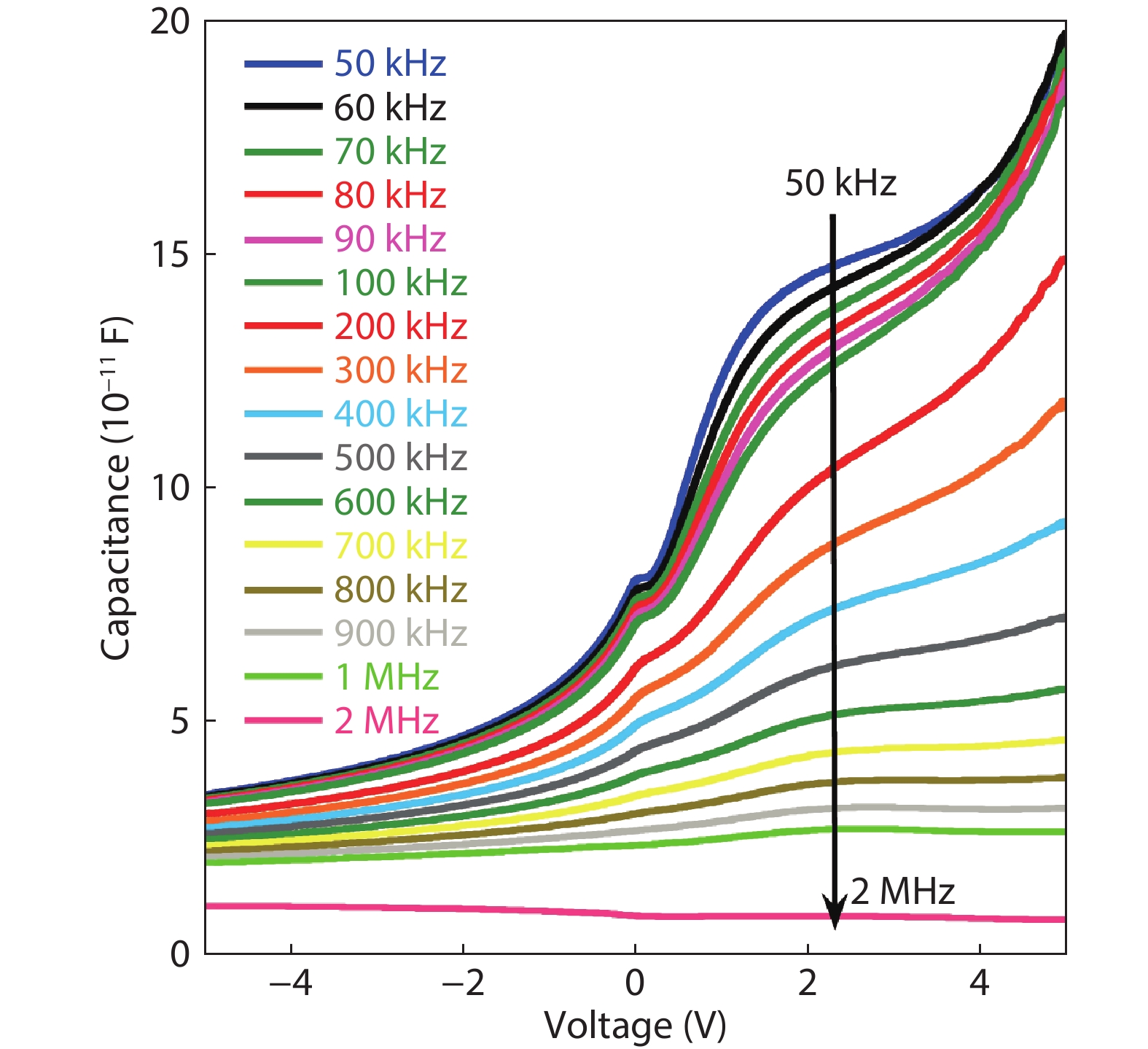
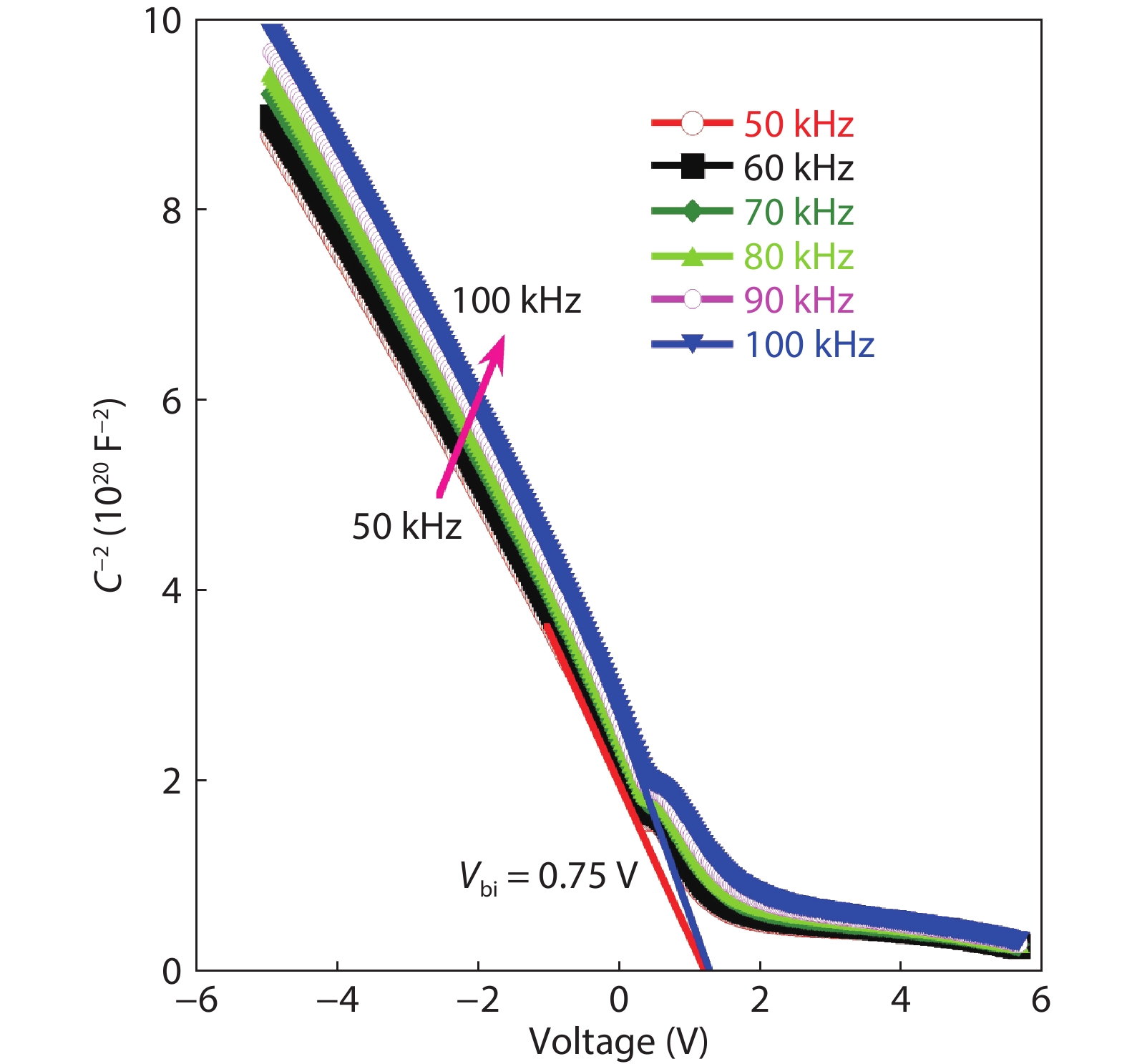
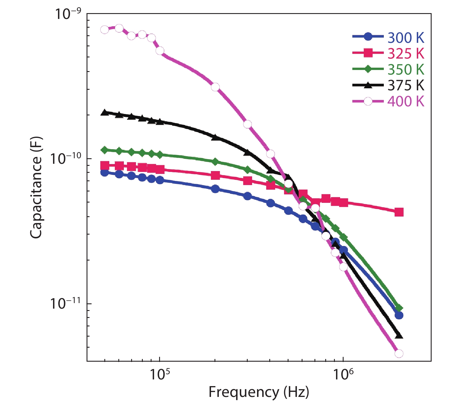
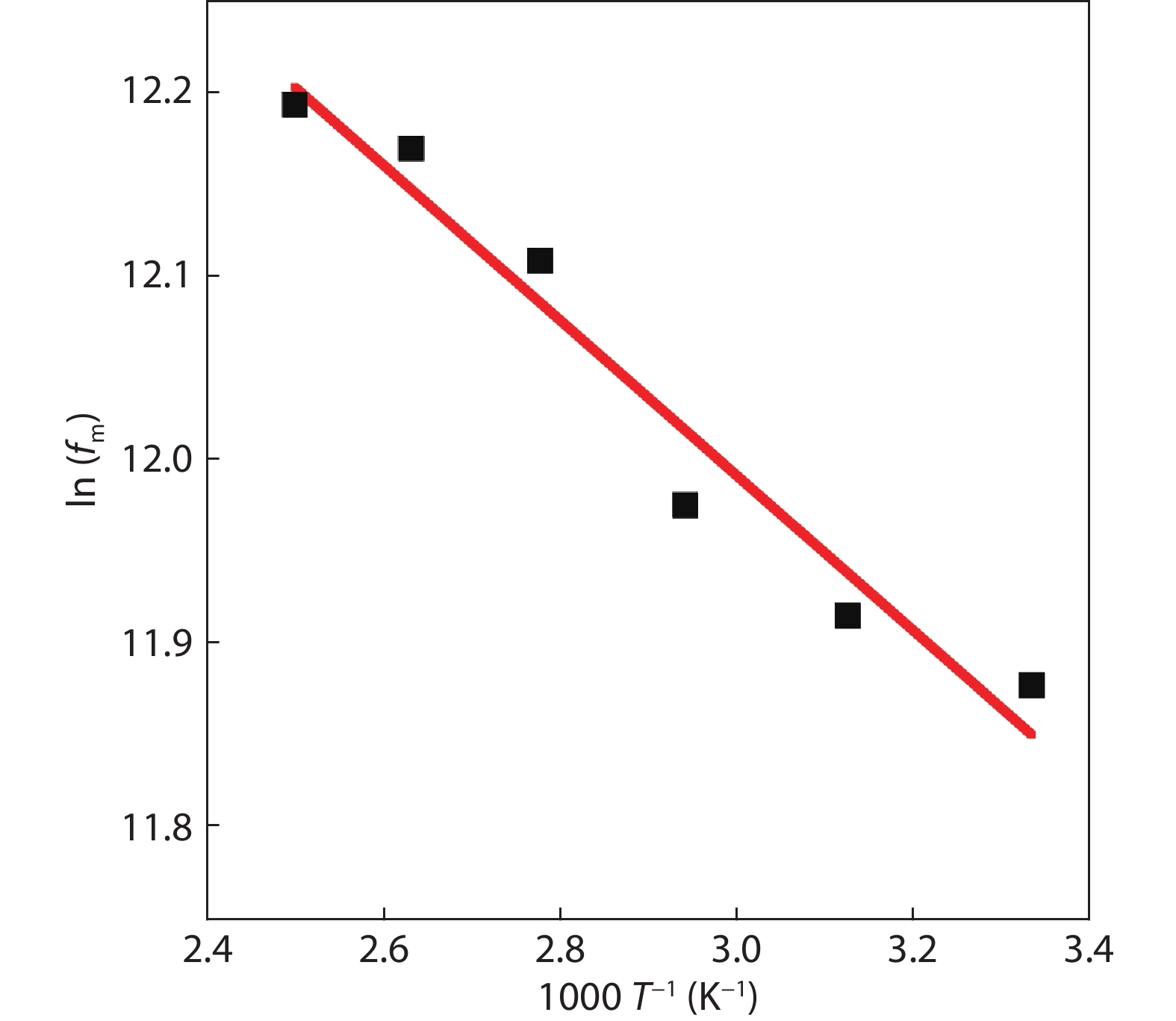
ARTICLES

Determination of trap density-of-states distribution of nitrogen-doped ultrananocrystalline diamond/hydrogenated amorphous carbon composite films

Mahmoud Shaban1, 2,

+ Author Affiliations

 Corresponding author: Mahmoud Shaban, s.mahmoud@qu.edu.sa, m_shaban@aswu.edu.eg

PDF

Turn off MathJax

Abstract: Thin films comprising nitrogen-doped ultrananocrystalline diamond/hydrogenated amorphous-carbon (UNCD/a-C:H) composite films were experimentally investigated. The prepared films were grown on Si substrates by the coaxial arc plasma deposition method. They were characterized by temperature-dependent capacitance-frequency measurements in the temperature and frequency ranges of 300–400 K and 50 kHz–2 MHz, respectively. The energy distribution of trap density of states in the films was extracted using a simple technique utilizing the measured capacitance-frequency characteristics. In the measured temperature range, the energy-distributed traps exhibited Gaussian-distributed states with peak values lie in the range: 2.84 × 10¹⁶–2.73 × 10¹⁷ eV–1 cm–3 and centered at energies of 120–233 meV below the conduction band. These states are generated due to a large amount of sp2-C and π-bond states, localized in GBs of the UNCD/a-C:H film. The attained defect parameters are accommodating to understand basic electrical properties of UNCD/a-C:H composite and can be adopted to suppress defects in the UNCD-based materials.

Key words: nitrogen-dopingnanodiamondUNCD/a-C:Hcapacitance-frequency characterizationtrap density-of-states


[1]
Koizumi S, Nebel C, Nesladek M. Physics and applications of CVD diamond. Weinheim: Wiley, 2008
[2]
May P W. Diamond thin films: A 21st-century material. Philos Trans Royal Soc Lond Ser A, 2000, 358, 473 doi: 10.1098/rsta.2000.0542
[3]
Mi S C, Kiss M, Graziosi T, et al. Integrated photonic devices in single crystal diamond. J Phys Photonics, 2020, 2, 042001 doi: 10.1088/2515-7647/aba171
[4]
Kobayashi A, Ohmagari S, Umezawa H, et al. Suppression of killer defects in diamond vertical-type Schottky barrier diodes. Jpn J Appl Phys, 2020, 59, SGGD10 doi: 10.7567/1347-4065/ab65b1
[5]
Matsumoto T, Kato H, Oyama K, et al. Inversion channel diamond metal-oxide-semiconductor field-effect transistor with normally off characteristics. Sci Rep, 2016, 6, 31585 doi: 10.1038/srep31585
[6]
Peng X Y, Li Y M, Duan S K, et al. Precise ultrananocrystalline diamond nanowire arrays for high performance gas sensing application. Mater Lett, 2020, 265, 127404 doi: 10.1016/j.matlet.2020.127404
[7]
Jiao S, Sumant A, Kirk M A, et al. Microstructure of ultrananocrystalline diamond films grown by microwave Ar–CH4 plasma chemical vapor deposition with or without added H2. J Appl Phys, 2001, 90, 118 doi: 10.1063/1.1377301
[8]
Bevilacqua M, Tumilty N, Mitra C, et al. Nanocrystalline diamond as an electronic material: An impedance spectroscopic and Hall effect measurement study. J Appl Phys, 2010, 107, 033716 doi: 10.1063/1.3291118
[9]
Auciello O, Sumant A V. Status review of the science and technology of ultrananocrystalline diamond (UNCD™) films and application to multifunctional devices. Diam Relat Mater, 2010, 19, 699 doi: 10.1016/j.diamond.2010.03.015
[10]
Zeng H J, Konicek A R, Moldovan N, et al. Boron-doped ultrananocrystalline diamond synthesized with an H-rich/Ar-lean gas system. Carbon, 2015, 84, 103 doi: 10.1016/j.carbon.2014.11.057
[11]
Mertens M, Mohr M, Wiora N, et al. N-type conductive ultrananocrystalline diamond films grown by hot filament CVD. J Nanomater, 2015, 2015, 1 doi: 10.1155/2015/527025
[12]
Ikeda T, Teii K, Casiraghi C, et al. Effect of the sp2 carbon phase on n-type conduction in nanodiamond films. J Appl Phys, 2008, 104, 073720 doi: 10.1063/1.2990061
[13]
Zapol P, Sternberg M, Curtiss L A, et al. Tight-binding molecular-dynamics simulation of impurities in ultrananocrystalline diamond grain boundaries. Phys Rev B, 2001, 65, 045403 doi: 10.1103/PhysRevB.65.045403
[14]
Bhattacharyya S, Auciello O, Birrell J, et al. Synthesis and characterization of highly-conducting nitrogen-doped ultrananocrystalline diamond films. Appl Phys Lett, 2001, 79, 1441 doi: 10.1063/1.1400761
[15]
Birrell J, Gerbi J E, Auciello O, et al. Bonding structure in nitrogen doped ultrananocrystalline diamond. J Appl Phys, 2003, 93, 5606 doi: 10.1063/1.1564880
[16]
Kulisch W, Popov C, Lefterova E, et al. Electrical properties of ultrananocrystalline diamond/amorphous carbon nanocomposite films. Diam Relat Mater, 2010, 19, 449 doi: 10.1016/j.diamond.2010.01.021
[17]
Voss A, Stateva S R, Reithmaier J P, et al. Patterning of the surface termination of ultrananocrystalline diamond films for guided cell attachment and growth. Surf Coat Technol, 2017, 321, 229 doi: 10.1016/j.surfcoat.2017.04.066
[18]
Hanada K, Nishiyama T, Yoshitake T, et al. Optical emission spectroscopy of deposition process of ultrananocrystalline diamond/hydrogenated amorphous carbon composite films by using a coaxial arc plasma gun. Diam Relat Mater, 2010, 19, 899 doi: 10.1016/j.diamond.2010.02.019
[19]
Chaleawpong R, Promros N, Zkria A, et al. Diode parameters and ultraviolet light detection characteristics of n-type silicon/p-type nanocrystalline diamond heterojunctions at different temperatures. Thin Solid Films, 2020, 709, 138222 doi: 10.1016/j.tsf.2020.138222
[20]
Ali A M, Deckert-Gaudig T, Egiza M, et al. Near- and far-field Raman spectroscopic studies of nanodiamond composite films deposited by coaxial arc plasma. Appl Phys Lett, 2020, 116, 041601 doi: 10.1063/1.5142198
[21]
Katamune Y, Al-Riyami S, Takeichi S, et al. Study on defects in ultrananocrystalline diamond/amorphous carbon composite films prepared by physical vapor deposition. ECS Trans, 2017, 75, 45 doi: 10.1149/07525.0045ecst
[22]
Zkria A, Abubakr E, Sittimart P, et al. Analysis of electrical characteristics of Pd/n-nanocarbon/p-Si heterojunction diodes: By CVf and G/wVf. J Nanomater, 2020, 2020, 4917946 doi: 10.1155/2020/4917946
[23]
Zkria A, Abdel-Wahab F, Katamune Y, et al. Optical and structural characterization of ultrananocrystalline diamond/hydrogenated amorphous carbon composite films deposited via coaxial arc plasma. Curr Appl Phys, 2019, 19, 143 doi: 10.1016/j.cap.2018.11.012
[24]
Al-Riyami S, Ohmagari S, Yoshitake T. Nitrogen-doped ultrananocrystalline diamond/hydrogenated amorphous carbon composite films prepared by pulsed laser deposition. Appl Phys Express, 2010, 3, 115102 doi: 10.1143/APEX.3.115102
[25]
Zkria A, Gima H, Shaban M, et al. Electrical characteristics of nitrogen-doped ultrananocrystalline diamond/hydrogenated amorphous carbon composite films prepared by coaxial arc plasma deposition. Appl Phys Express, 2015, 8, 095101 doi: 10.7567/APEX.8.095101
[26]
Gima H, Zkria A, Katamune Y, et al. Chemical bonding structural analysis of nitrogen-doped ultrananocrystalline diamond/hydrogenated amorphous carbon composite films prepared by coaxial arc plasma deposition. Appl Phys Express, 2017, 10, 015801 doi: 10.7567/APEX.10.015801
[27]
Zkria A, Shaban M, Hanada T, et al. Current transport mechanisms in N-type ultrananocrystalline diamond/p-type Si heterojunctions. J Nanosci Nanotechnol, 2016, 16, 12749 doi: 10.1166/jnn.2016.13663
[28]
Zkria A, Gima H, Yoshitake T. Application of nitrogen-doped ultrananocrystalline diamond/hydrogenated amorphous carbon composite films for ultraviolet detection. Appl Phys A, 2017, 123, 167 doi: 10.1007/s00339-017-0798-4
[29]
Zkria A, Yoshitake T. Temperature-dependent current–voltage characteristics and ultraviolet light detection of heterojunction diodes comprising n-type ultrananocrystalline diamond/hydrogenated amorphous carbon composite films and p-type silicon substrates. Jpn J Appl Phys, 2017, 56, 07KD04 doi: 10.7567/JJAP.56.07KD04
[30]
Shaban M, Zkria A, Yoshitake T. Characterization and design optimization of heterojunction photodiodes comprising n-type ultrananocrystalline diamond/hydrogenated amorphous carbon composite and p-type Si. Mater Sci Semicond Process, 2018, 86, 115 doi: 10.1016/j.mssp.2018.06.028
[31]
Zkria A, Shaban M, Abubakr E, et al. Impedance spectroscopy analysis of n-type (nitrogen-doped) ultrananocrystalline diamond/p-type Si heterojunction diodes. Phys Scr, 2020, 95, 095803 doi: 10.1088/1402-4896/aba97e
[32]
Shaban M. Modeling, design, and simulation of Schottky diodes based on ultrananocrystalline diamond composite films. Semicond Sci Technol, 2020, 36(1), 015004 doi: 10.1088/1361-6641/abc28e
[33]
Sze S M, Ng K K. Physics of semiconductor devices. Hoboken, NJ, USA: John Wiley & Sons, Inc., 2006
[34]
Schroder D K. Semiconductor material and device characterization. Hoboken, NJ, USA: John Wiley & Sons, Inc., 2005
[35]
Carr J A, Elshobaki M, Chaudhary S. Deep defects and the attempt to escape frequency in organic photovoltaic materials. Appl Phys Lett, 2015, 107, 203302 doi: 10.1063/1.4936160
[36]
Makino T, Kato H, Ri S G, et al. Electrical characterization of homoepitaxial diamond p-n+ junction. Diam Relat Mater, 2005, 14, 1995 doi: 10.1016/j.diamond.2005.07.019
[37]
Zhang X F, Matsumoto T, Sakurai U, et al. Energy distribution of Al2O3/diamond interface states characterized by high temperature capacitance-voltage method. Carbon, 2020, 168, 659 doi: 10.1016/j.carbon.2020.07.019
[38]
Xu H, Ye H T, Coathup D, et al. An insight of p-type to n-type conductivity conversion in oxygen ion-implanted ultrananocrystalline diamond films by impedance spectroscopy. Appl Phys Lett, 2017, 110, 033102 doi: 10.1063/1.4974077
[39]
Frolov V D, Pimenov S M, Konov V I, Polyakov, et al. Electronic properties of low-field-emitting ultrananocrystalline diamond films. Surf Interface Anal, 2004, 36, 449 doi: 10.1002/sia.1709
[40]
Wiora N, Mertens M, Brühne K, et al. Grain boundary dominated electrical conductivity in ultrananocrystalline diamond. J Appl Phys, 2017, 122, 145102 doi: 10.1063/1.4993442
[41]
Walter T, Herberholz R, Muller C, et al. Determination of defect distributions from admittance measurements and application to Cu(In, Ga)Se2 based heterojunctions. J Appl Phys, 1996, 80, 4411 doi: 10.1063/1.363401
Fig. 1.  (Color online) (a) Top-view FESEM images, (b) AFM image of UNCD/a-C:H film surface, (c) cross-sectional FESEM image, (d) schematic representation, and (e) semi-logarithmic and linear (inset) JV characteristics of N2-doped (UNCD/a-C:H)/p-Si heterojunctions.

Fig. 2.  (Color online) CV characteristics of (N2-doped UNCD/a-C:H)/p-type Si heterojunction, measured at different frequencies from 50 kHz to 2 MHz.

Fig. 3.  (Color online) CV characteristics of (N2-doped UNCD/a-C:H)/p-type Si heterojunction, measured at different frequencies from 50 to 100 kHz.

Fig. 4.  (Color online) Zr and Zim spectra of (N2-doped UNCD/a-C:H)/p-type Si heterojunction, measured at different temperatures from 300 to 400 K.

Fig. 5.  (Color online) Cf characteristics of (N2-doped UNCD/a-C:H)/p-type Si heterojunction, measured at different temperatures.

Fig. 6.  Arrhenius plot of ln(fm) of (N2-doped UNCD/a-C:H)/p-type Si heterojunction.

Fig. 7.  Energy-distributed trap-DOS of N2-doped UNCD/a-C:H film measured (dots) and fitted (lines) data at temperatures of (a) 300 K, (b) 325 K, (c) 350 K, (d) 375 K, and (e) 400 K.

Table 1.   Extracted Gaussian-distributed defect parameters of N2-doped UNCD/a-C:H films characterized at different temperatures.

T (K)NG (1016 cm–3 eV–1)Et (eV)σ (eV)
3002.84 0.1200.064
3251.56 0.1580.058
3504.48 0.1590.041
3757.12 0.1890.050
40027.3 0.2330.050
DownLoad: CSV
[1]
Koizumi S, Nebel C, Nesladek M. Physics and applications of CVD diamond. Weinheim: Wiley, 2008
[2]
May P W. Diamond thin films: A 21st-century material. Philos Trans Royal Soc Lond Ser A, 2000, 358, 473 doi: 10.1098/rsta.2000.0542
[3]
Mi S C, Kiss M, Graziosi T, et al. Integrated photonic devices in single crystal diamond. J Phys Photonics, 2020, 2, 042001 doi: 10.1088/2515-7647/aba171
[4]
Kobayashi A, Ohmagari S, Umezawa H, et al. Suppression of killer defects in diamond vertical-type Schottky barrier diodes. Jpn J Appl Phys, 2020, 59, SGGD10 doi: 10.7567/1347-4065/ab65b1
[5]
Matsumoto T, Kato H, Oyama K, et al. Inversion channel diamond metal-oxide-semiconductor field-effect transistor with normally off characteristics. Sci Rep, 2016, 6, 31585 doi: 10.1038/srep31585
[6]
Peng X Y, Li Y M, Duan S K, et al. Precise ultrananocrystalline diamond nanowire arrays for high performance gas sensing application. Mater Lett, 2020, 265, 127404 doi: 10.1016/j.matlet.2020.127404
[7]
Jiao S, Sumant A, Kirk M A, et al. Microstructure of ultrananocrystalline diamond films grown by microwave Ar–CH4 plasma chemical vapor deposition with or without added H2. J Appl Phys, 2001, 90, 118 doi: 10.1063/1.1377301
[8]
Bevilacqua M, Tumilty N, Mitra C, et al. Nanocrystalline diamond as an electronic material: An impedance spectroscopic and Hall effect measurement study. J Appl Phys, 2010, 107, 033716 doi: 10.1063/1.3291118
[9]
Auciello O, Sumant A V. Status review of the science and technology of ultrananocrystalline diamond (UNCD™) films and application to multifunctional devices. Diam Relat Mater, 2010, 19, 699 doi: 10.1016/j.diamond.2010.03.015
[10]
Zeng H J, Konicek A R, Moldovan N, et al. Boron-doped ultrananocrystalline diamond synthesized with an H-rich/Ar-lean gas system. Carbon, 2015, 84, 103 doi: 10.1016/j.carbon.2014.11.057
[11]
Mertens M, Mohr M, Wiora N, et al. N-type conductive ultrananocrystalline diamond films grown by hot filament CVD. J Nanomater, 2015, 2015, 1 doi: 10.1155/2015/527025
[12]
Ikeda T, Teii K, Casiraghi C, et al. Effect of the sp2 carbon phase on n-type conduction in nanodiamond films. J Appl Phys, 2008, 104, 073720 doi: 10.1063/1.2990061
[13]
Zapol P, Sternberg M, Curtiss L A, et al. Tight-binding molecular-dynamics simulation of impurities in ultrananocrystalline diamond grain boundaries. Phys Rev B, 2001, 65, 045403 doi: 10.1103/PhysRevB.65.045403
[14]
Bhattacharyya S, Auciello O, Birrell J, et al. Synthesis and characterization of highly-conducting nitrogen-doped ultrananocrystalline diamond films. Appl Phys Lett, 2001, 79, 1441 doi: 10.1063/1.1400761
[15]
Birrell J, Gerbi J E, Auciello O, et al. Bonding structure in nitrogen doped ultrananocrystalline diamond. J Appl Phys, 2003, 93, 5606 doi: 10.1063/1.1564880
[16]
Kulisch W, Popov C, Lefterova E, et al. Electrical properties of ultrananocrystalline diamond/amorphous carbon nanocomposite films. Diam Relat Mater, 2010, 19, 449 doi: 10.1016/j.diamond.2010.01.021
[17]
Voss A, Stateva S R, Reithmaier J P, et al. Patterning of the surface termination of ultrananocrystalline diamond films for guided cell attachment and growth. Surf Coat Technol, 2017, 321, 229 doi: 10.1016/j.surfcoat.2017.04.066
[18]
Hanada K, Nishiyama T, Yoshitake T, et al. Optical emission spectroscopy of deposition process of ultrananocrystalline diamond/hydrogenated amorphous carbon composite films by using a coaxial arc plasma gun. Diam Relat Mater, 2010, 19, 899 doi: 10.1016/j.diamond.2010.02.019
[19]
Chaleawpong R, Promros N, Zkria A, et al. Diode parameters and ultraviolet light detection characteristics of n-type silicon/p-type nanocrystalline diamond heterojunctions at different temperatures. Thin Solid Films, 2020, 709, 138222 doi: 10.1016/j.tsf.2020.138222
[20]
Ali A M, Deckert-Gaudig T, Egiza M, et al. Near- and far-field Raman spectroscopic studies of nanodiamond composite films deposited by coaxial arc plasma. Appl Phys Lett, 2020, 116, 041601 doi: 10.1063/1.5142198
[21]
Katamune Y, Al-Riyami S, Takeichi S, et al. Study on defects in ultrananocrystalline diamond/amorphous carbon composite films prepared by physical vapor deposition. ECS Trans, 2017, 75, 45 doi: 10.1149/07525.0045ecst
[22]
Zkria A, Abubakr E, Sittimart P, et al. Analysis of electrical characteristics of Pd/n-nanocarbon/p-Si heterojunction diodes: By CVf and G/wVf. J Nanomater, 2020, 2020, 4917946 doi: 10.1155/2020/4917946
[23]
Zkria A, Abdel-Wahab F, Katamune Y, et al. Optical and structural characterization of ultrananocrystalline diamond/hydrogenated amorphous carbon composite films deposited via coaxial arc plasma. Curr Appl Phys, 2019, 19, 143 doi: 10.1016/j.cap.2018.11.012
[24]
Al-Riyami S, Ohmagari S, Yoshitake T. Nitrogen-doped ultrananocrystalline diamond/hydrogenated amorphous carbon composite films prepared by pulsed laser deposition. Appl Phys Express, 2010, 3, 115102 doi: 10.1143/APEX.3.115102
[25]
Zkria A, Gima H, Shaban M, et al. Electrical characteristics of nitrogen-doped ultrananocrystalline diamond/hydrogenated amorphous carbon composite films prepared by coaxial arc plasma deposition. Appl Phys Express, 2015, 8, 095101 doi: 10.7567/APEX.8.095101
[26]
Gima H, Zkria A, Katamune Y, et al. Chemical bonding structural analysis of nitrogen-doped ultrananocrystalline diamond/hydrogenated amorphous carbon composite films prepared by coaxial arc plasma deposition. Appl Phys Express, 2017, 10, 015801 doi: 10.7567/APEX.10.015801
[27]
Zkria A, Shaban M, Hanada T, et al. Current transport mechanisms in N-type ultrananocrystalline diamond/p-type Si heterojunctions. J Nanosci Nanotechnol, 2016, 16, 12749 doi: 10.1166/jnn.2016.13663
[28]
Zkria A, Gima H, Yoshitake T. Application of nitrogen-doped ultrananocrystalline diamond/hydrogenated amorphous carbon composite films for ultraviolet detection. Appl Phys A, 2017, 123, 167 doi: 10.1007/s00339-017-0798-4
[29]
Zkria A, Yoshitake T. Temperature-dependent current–voltage characteristics and ultraviolet light detection of heterojunction diodes comprising n-type ultrananocrystalline diamond/hydrogenated amorphous carbon composite films and p-type silicon substrates. Jpn J Appl Phys, 2017, 56, 07KD04 doi: 10.7567/JJAP.56.07KD04
[30]
Shaban M, Zkria A, Yoshitake T. Characterization and design optimization of heterojunction photodiodes comprising n-type ultrananocrystalline diamond/hydrogenated amorphous carbon composite and p-type Si. Mater Sci Semicond Process, 2018, 86, 115 doi: 10.1016/j.mssp.2018.06.028
[31]
Zkria A, Shaban M, Abubakr E, et al. Impedance spectroscopy analysis of n-type (nitrogen-doped) ultrananocrystalline diamond/p-type Si heterojunction diodes. Phys Scr, 2020, 95, 095803 doi: 10.1088/1402-4896/aba97e
[32]
Shaban M. Modeling, design, and simulation of Schottky diodes based on ultrananocrystalline diamond composite films. Semicond Sci Technol, 2020, 36(1), 015004 doi: 10.1088/1361-6641/abc28e
[33]
Sze S M, Ng K K. Physics of semiconductor devices. Hoboken, NJ, USA: John Wiley & Sons, Inc., 2006
[34]
Schroder D K. Semiconductor material and device characterization. Hoboken, NJ, USA: John Wiley & Sons, Inc., 2005
[35]
Carr J A, Elshobaki M, Chaudhary S. Deep defects and the attempt to escape frequency in organic photovoltaic materials. Appl Phys Lett, 2015, 107, 203302 doi: 10.1063/1.4936160
[36]
Makino T, Kato H, Ri S G, et al. Electrical characterization of homoepitaxial diamond p-n+ junction. Diam Relat Mater, 2005, 14, 1995 doi: 10.1016/j.diamond.2005.07.019
[37]
Zhang X F, Matsumoto T, Sakurai U, et al. Energy distribution of Al2O3/diamond interface states characterized by high temperature capacitance-voltage method. Carbon, 2020, 168, 659 doi: 10.1016/j.carbon.2020.07.019
[38]
Xu H, Ye H T, Coathup D, et al. An insight of p-type to n-type conductivity conversion in oxygen ion-implanted ultrananocrystalline diamond films by impedance spectroscopy. Appl Phys Lett, 2017, 110, 033102 doi: 10.1063/1.4974077
[39]
Frolov V D, Pimenov S M, Konov V I, Polyakov, et al. Electronic properties of low-field-emitting ultrananocrystalline diamond films. Surf Interface Anal, 2004, 36, 449 doi: 10.1002/sia.1709
[40]
Wiora N, Mertens M, Brühne K, et al. Grain boundary dominated electrical conductivity in ultrananocrystalline diamond. J Appl Phys, 2017, 122, 145102 doi: 10.1063/1.4993442
[41]
Walter T, Herberholz R, Muller C, et al. Determination of defect distributions from admittance measurements and application to Cu(In, Ga)Se2 based heterojunctions. J Appl Phys, 1996, 80, 4411 doi: 10.1063/1.363401
  • Search

    Advanced Search >>

    GET CITATION

    shu

    Export: BibTex EndNote

    Article Metrics

    Article views: 2048 Times PDF downloads: 78 Times Cited by: 0 Times

    History

    Received: 12 November 2020 Revised: 11 December 2020 Online: Accepted Manuscript: 01 February 2021Uncorrected proof: 22 February 2021Published: 01 June 2021

    Catalog

      Email This Article

      User name:
      Email:*请输入正确邮箱
      Code:*验证码错误
      Mahmoud Shaban. Determination of trap density-of-states distribution of nitrogen-doped ultrananocrystalline diamond/hydrogenated amorphous carbon composite films[J]. Journal of Semiconductors, 2021, 42(6): 062802. doi: 10.1088/1674-4926/42/6/062802 M Shaban, Determination of trap density-of-states distribution of nitrogen-doped ultrananocrystalline diamond/hydrogenated amorphous carbon composite films[J]. J. Semicond., 2021, 42(6): 062802. doi: 10.1088/1674-4926/42/6/062802.Export: BibTex EndNote
      Citation:
      Mahmoud Shaban. Determination of trap density-of-states distribution of nitrogen-doped ultrananocrystalline diamond/hydrogenated amorphous carbon composite films[J]. Journal of Semiconductors, 2021, 42(6): 062802. doi: 10.1088/1674-4926/42/6/062802

      M Shaban, Determination of trap density-of-states distribution of nitrogen-doped ultrananocrystalline diamond/hydrogenated amorphous carbon composite films[J]. J. Semicond., 2021, 42(6): 062802. doi: 10.1088/1674-4926/42/6/062802.
      Export: BibTex EndNote

      Determination of trap density-of-states distribution of nitrogen-doped ultrananocrystalline diamond/hydrogenated amorphous carbon composite films

      doi: 10.1088/1674-4926/42/6/062802
      More Information
      • Author Bio:

        Mahmoud Shaban was born in Luxor, Egypt. He received the B.Eng. degree in electrical engineering, specializing in electronics and communications, from Assiut University, Assiut, Egypt, in 1998, the M.Sc. degree in electronics from South Valley University, Aswan, Egypt, in 2003, and the Ph.D. degree in applied science for electronics and materials from Kyushu University, Fukuoka, Japan, in 2009. He is currently an Associate Professor with the Department of Electrical Engineering, Faculty of Engineering, Aswan University. He is also with the Department of Electrical Engineering, College of Engineering, Qassim University, Unaizah. His research interests include electronic materials, and electronic and optoelectronic devices

      • Corresponding author: s.mahmoud@qu.edu.sa, m_shaban@aswu.edu.eg
      • Received Date: 2020-11-12
      • Revised Date: 2020-12-11
      • Published Date: 2021-06-10

      Catalog

        /

        DownLoad:  Full-Size Img  PowerPoint
        Return
        Return