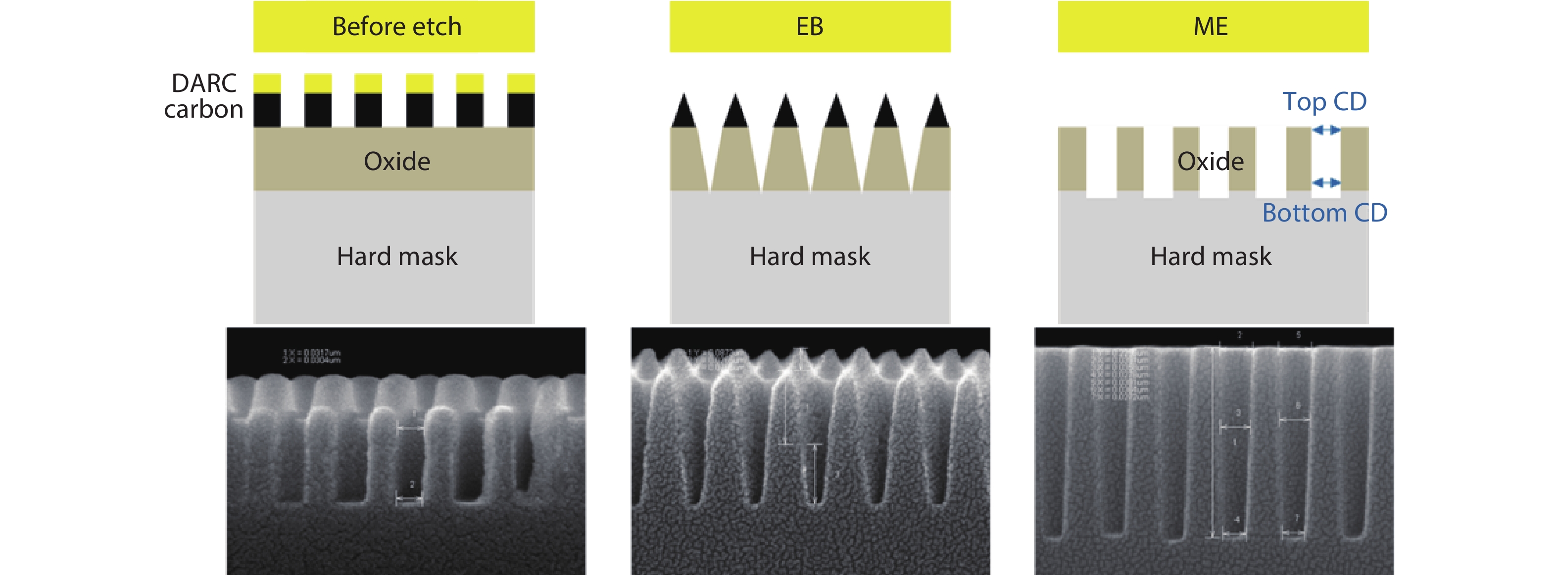
Fig. 1.
The strategy of etching oxide mask in the DRAM capacitor.
ARTICLES
Jianqiu Hou1, Zengwen Hu1, , Kuowen Lai2, Yule Sun2, Bo Shao2, Chunyang Wang2, Xinran Liu2 and Karson Liu2,
Corresponding author: Zengwen Hu, ZengwenHu@amecnsh.com; Karson Liu, Karson.Liu@cxmt.com
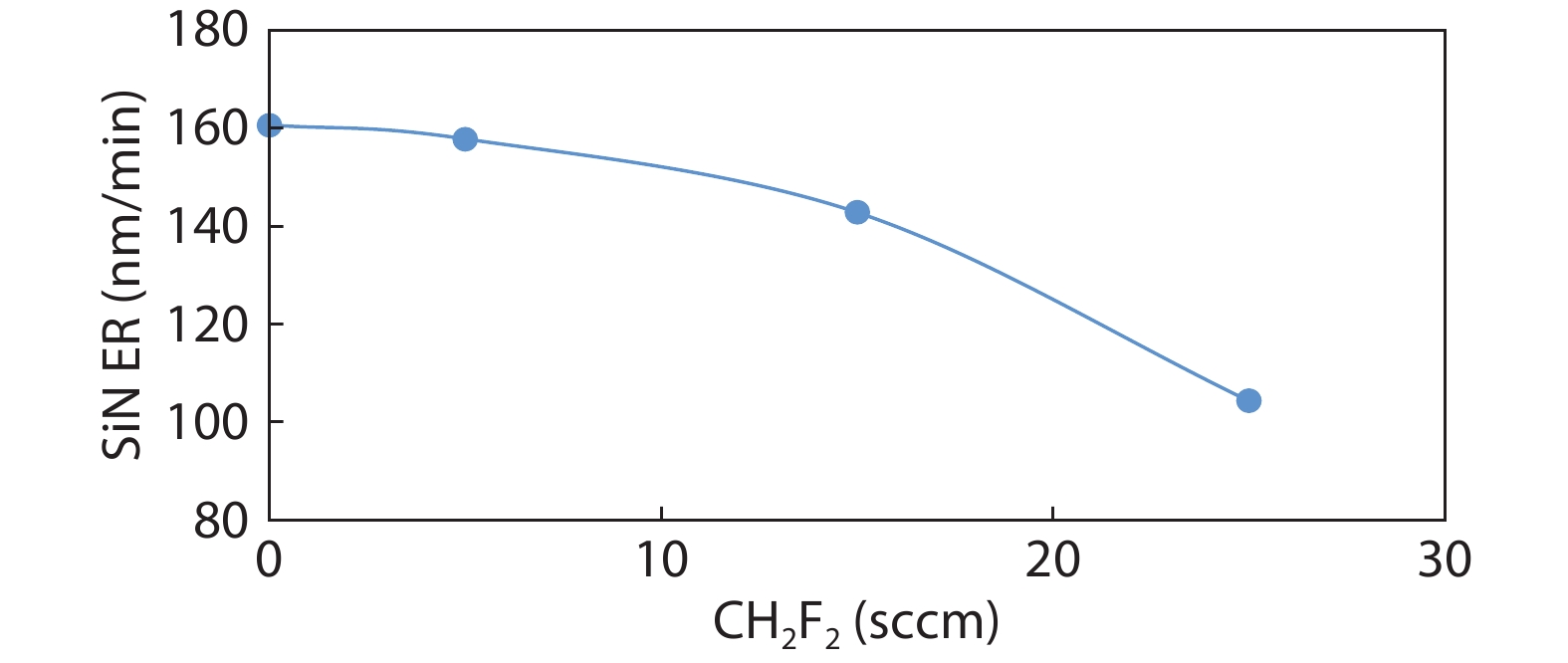
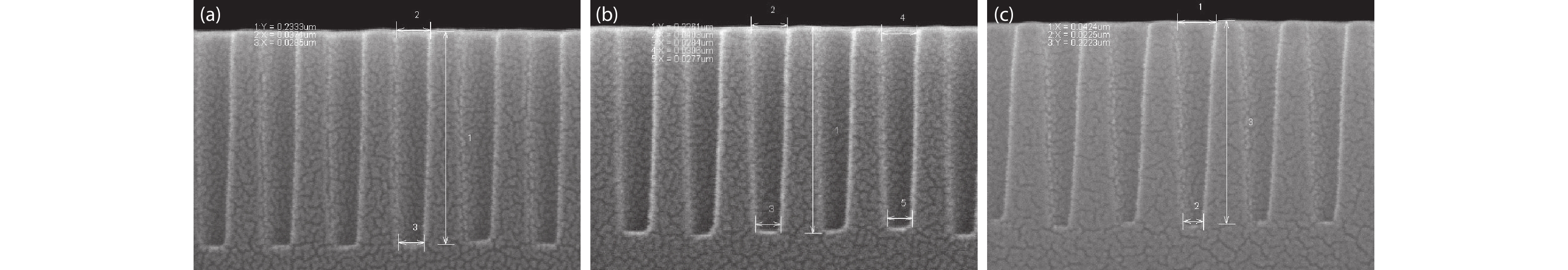
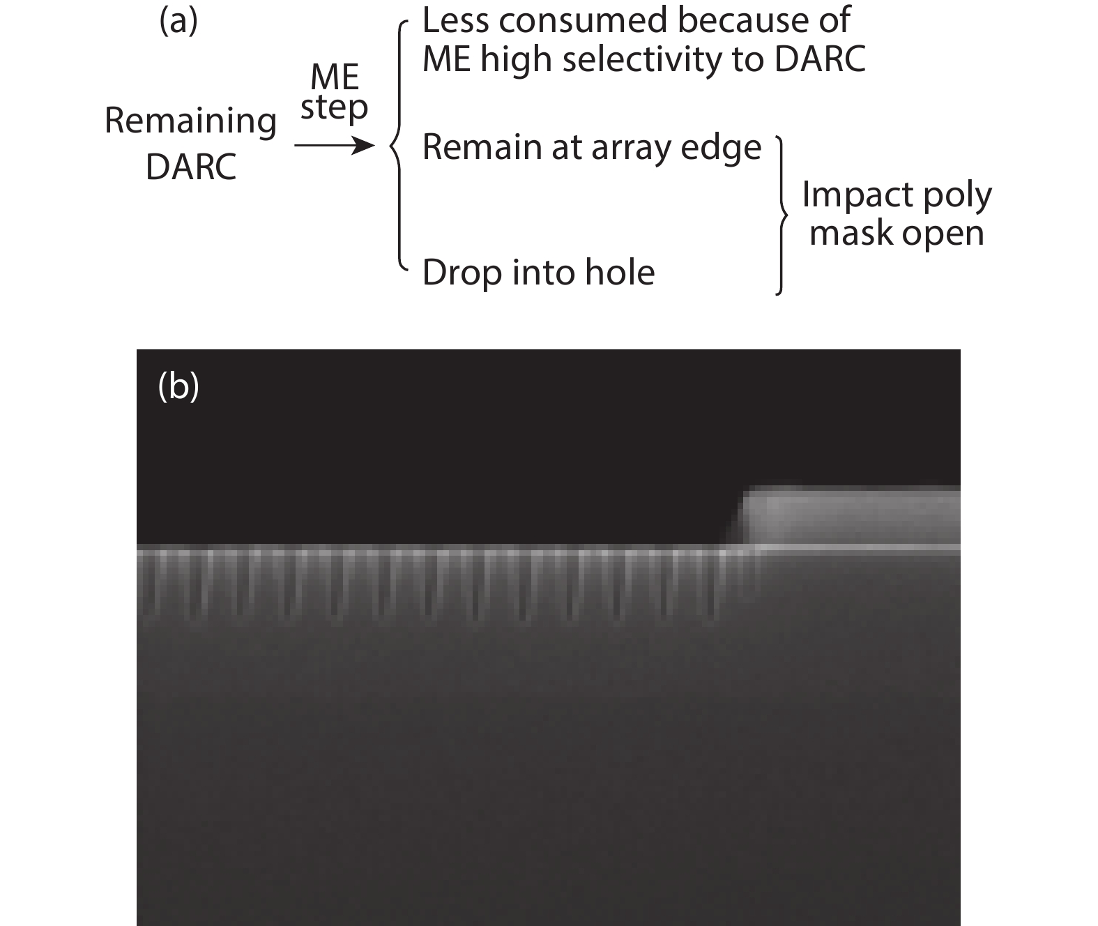
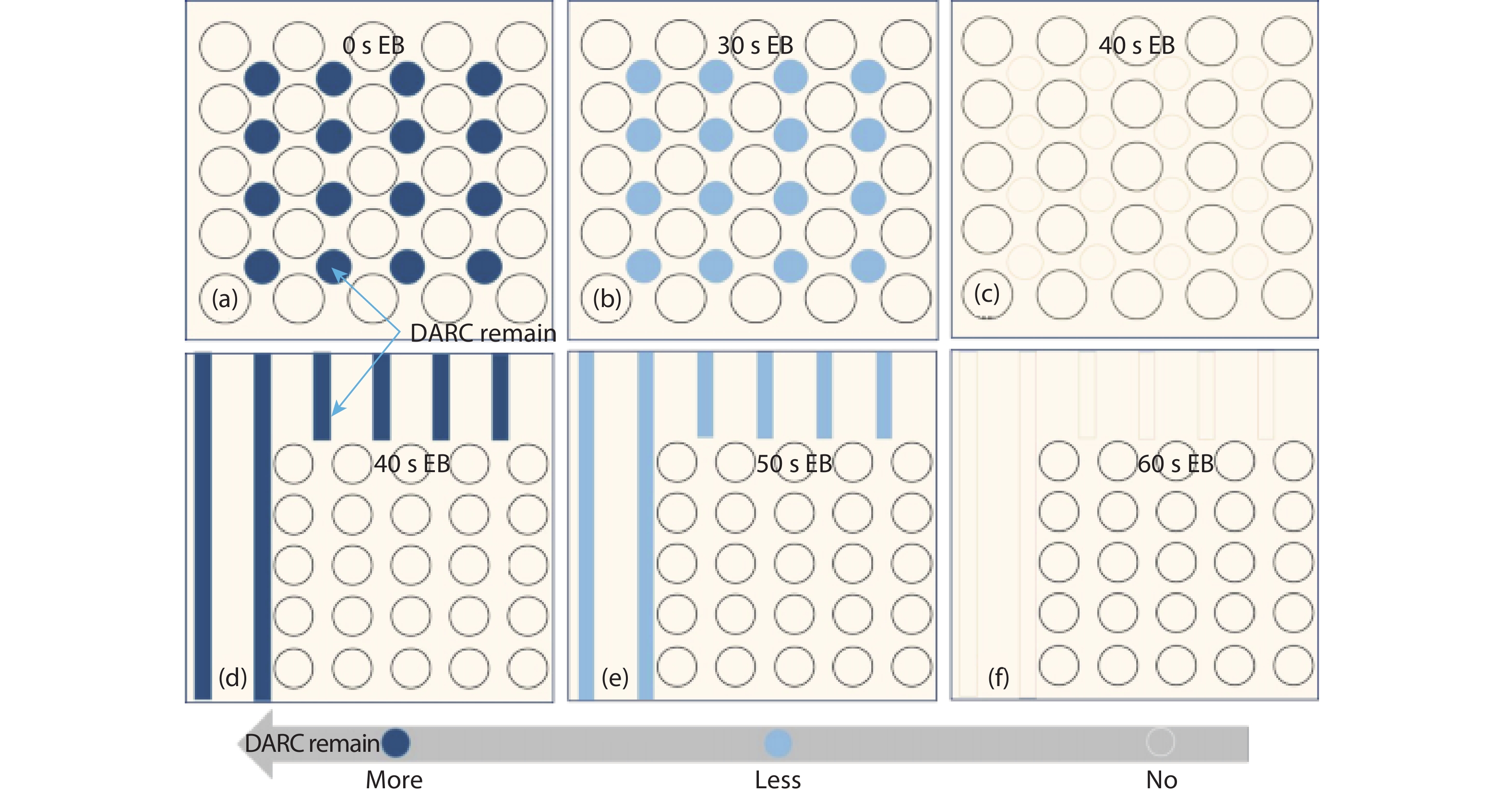
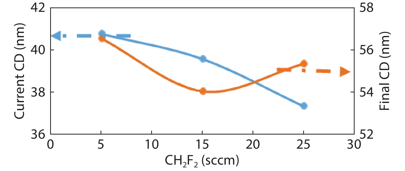
Abstract: Opening the silicon oxide mask of a capacitor in dynamic random access memory is a critical process on a capacitive coupled plasma (CCP) etch tool. Three steps, dielectric anti-reflective coating (DARC) etch back, silicon oxide etch and strip, are contained. To acquire good performance, such as low leakage current and high capacitance, for further fabricating capacitors, we should firstly optimize DARC etch back. We developed some experiments, focusing on etch time and chemistry, to evaluate the profile of a silicon oxide mask, DARC remain and critical dimension. The result shows that etch back time should be controlled in the range from 50 to 60 s, based on the current equipment and condition. It will make B/T ratio higher than 70% meanwhile resolve the DARC remain issue. We also found that CH2F2 flow should be ~15 sccm to avoid reversed CD trend and keep inline CD.
Key words: dynamic random access memory (DRAM), oxide mask open of capacitor, capacitive coupled plasma (CCP) etch, dielectric anti-reflective coating (DARC), etch back (EB)
| [1] |
Park J M, Hwang Y S, Kim S W, et al. 20 nm DRAM: A new beginning of another revolution. 2015 IEEE International Electron Devices Meeting (IEDM), 2015, 26
|
| [2] |
Kim Y, Lee S, Jung T, et al. Challenges in high-aspect ratio contact (HARC) etching for DRAM capacitor formation. Proc SPIE, 2015, 9428, 942806 doi: 10.1117/12.2087765
|
| [3] |
Lee J M, Choi P H, Kim S K, et al. New method for reduction of the capacitor leakage failure rate without changing the capacitor structure or materials in DRAM mass production. IEEE Trans Electron Devices, 2018, 65, 4839 doi: 10.1109/TED.2018.2870141
|
| [4] |
Kotecki D E. A review of high dielectric materials for DRAM capacitors. Integr Ferroelectr, 1997, 16, 1 doi: 10.1080/10584589708013025
|
| [5] |
Negreanu M, Gavrila R, Dinescu A. Tapered windows in silicon dioxide layers for masking and passivation: Obtaining and characterization methods. 1997 International Semiconductor Conference, 1997, 243
|
| [6] |
Chun I, Efremov A, Yeom G Y, et al. A comparative study of CF4/O2/Ar and C4F8/O2/Ar plasmas for dry etching applications. Thin Solid Films, 2015, 579, 136 doi: 10.1016/j.tsf.2015.02.060
|
| [7] |
Kastenmeier B E E, Matsuo P J, Beulens J J, et al. Chemical dry etching of silicon nitride and silicon dioxide using CF4/O2/N2 gas mixtures. J Vac Sci Technol A, 1996, 14, 2802 doi: 10.1116/1.580203
|
| [8] |
Standaert T E F M, Hedlund C, Joseph E A, et al. Role of fluorocarbon film formation in the etching of silicon, silicon dioxide, silicon nitride, and amorphous hydrogenated silicon carbide. J Vac Sci Technol A, 2004, 22, 53 doi: 10.1116/1.1626642
|
| [9] |
Mogab C J, Adams A C, Flamm D L. Plasma etching of Si and SiO2—The effect of oxygen additions to CF4 plasmas. J Appl Phys, 1978, 49, 3796 doi: 10.1063/1.325382
|


Article views: 5793 Times PDF downloads: 239 Times Cited by: 0 Times
Received: 15 January 2021 Revised: 11 March 2021 Online: Accepted Manuscript: 23 April 2021Uncorrected proof: 30 April 2021Published: 05 July 2021
| Citation: |
Jianqiu Hou, Zengwen Hu, Kuowen Lai, Yule Sun, Bo Shao, Chunyang Wang, Xinran Liu, Karson Liu. The investigation of DARC etch back in DRAM capacitor oxide mask opening[J]. Journal of Semiconductors, 2021, 42(7): 074101. doi: 10.1088/1674-4926/42/7/074101
J Q Hou, Z W Hu, K W Lai, Y L Sun, B Shao, C Y Wang, X R Liu, K Liu, The investigation of DARC etch back in DRAM capacitor oxide mask opening[J]. J. Semicond., 2021, 42(7): 074101. doi: 10.1088/1674-4926/42/7/074101.
Export: BibTex EndNote

|
| [1] |
Park J M, Hwang Y S, Kim S W, et al. 20 nm DRAM: A new beginning of another revolution. 2015 IEEE International Electron Devices Meeting (IEDM), 2015, 26
|
| [2] |
Kim Y, Lee S, Jung T, et al. Challenges in high-aspect ratio contact (HARC) etching for DRAM capacitor formation. Proc SPIE, 2015, 9428, 942806 doi: 10.1117/12.2087765
|
| [3] |
Lee J M, Choi P H, Kim S K, et al. New method for reduction of the capacitor leakage failure rate without changing the capacitor structure or materials in DRAM mass production. IEEE Trans Electron Devices, 2018, 65, 4839 doi: 10.1109/TED.2018.2870141
|
| [4] |
Kotecki D E. A review of high dielectric materials for DRAM capacitors. Integr Ferroelectr, 1997, 16, 1 doi: 10.1080/10584589708013025
|
| [5] |
Negreanu M, Gavrila R, Dinescu A. Tapered windows in silicon dioxide layers for masking and passivation: Obtaining and characterization methods. 1997 International Semiconductor Conference, 1997, 243
|
| [6] |
Chun I, Efremov A, Yeom G Y, et al. A comparative study of CF4/O2/Ar and C4F8/O2/Ar plasmas for dry etching applications. Thin Solid Films, 2015, 579, 136 doi: 10.1016/j.tsf.2015.02.060
|
| [7] |
Kastenmeier B E E, Matsuo P J, Beulens J J, et al. Chemical dry etching of silicon nitride and silicon dioxide using CF4/O2/N2 gas mixtures. J Vac Sci Technol A, 1996, 14, 2802 doi: 10.1116/1.580203
|
| [8] |
Standaert T E F M, Hedlund C, Joseph E A, et al. Role of fluorocarbon film formation in the etching of silicon, silicon dioxide, silicon nitride, and amorphous hydrogenated silicon carbide. J Vac Sci Technol A, 2004, 22, 53 doi: 10.1116/1.1626642
|
| [9] |
Mogab C J, Adams A C, Flamm D L. Plasma etching of Si and SiO2—The effect of oxygen additions to CF4 plasmas. J Appl Phys, 1978, 49, 3796 doi: 10.1063/1.325382
|

 WeChat ID
Journal of Semiconductors © 2017 All Rights Reserved 京ICP备05085259号-2

 DownLoad: