


Fig. 1.
(Color online) The cross-section schematic of the AlGaN/GaN HEMT.
ARTICLES
Changxi Chen1, 2, Quan Wang1, 3, Wei Li1, Qian Wang1, Chun Feng1, 2, Lijuan Jiang1, 2, Hongling Xiao1, 2 and Xiaoliang Wang1, 2,
Corresponding author: Xiaoliang Wang, xlwang@semi.ac.cn
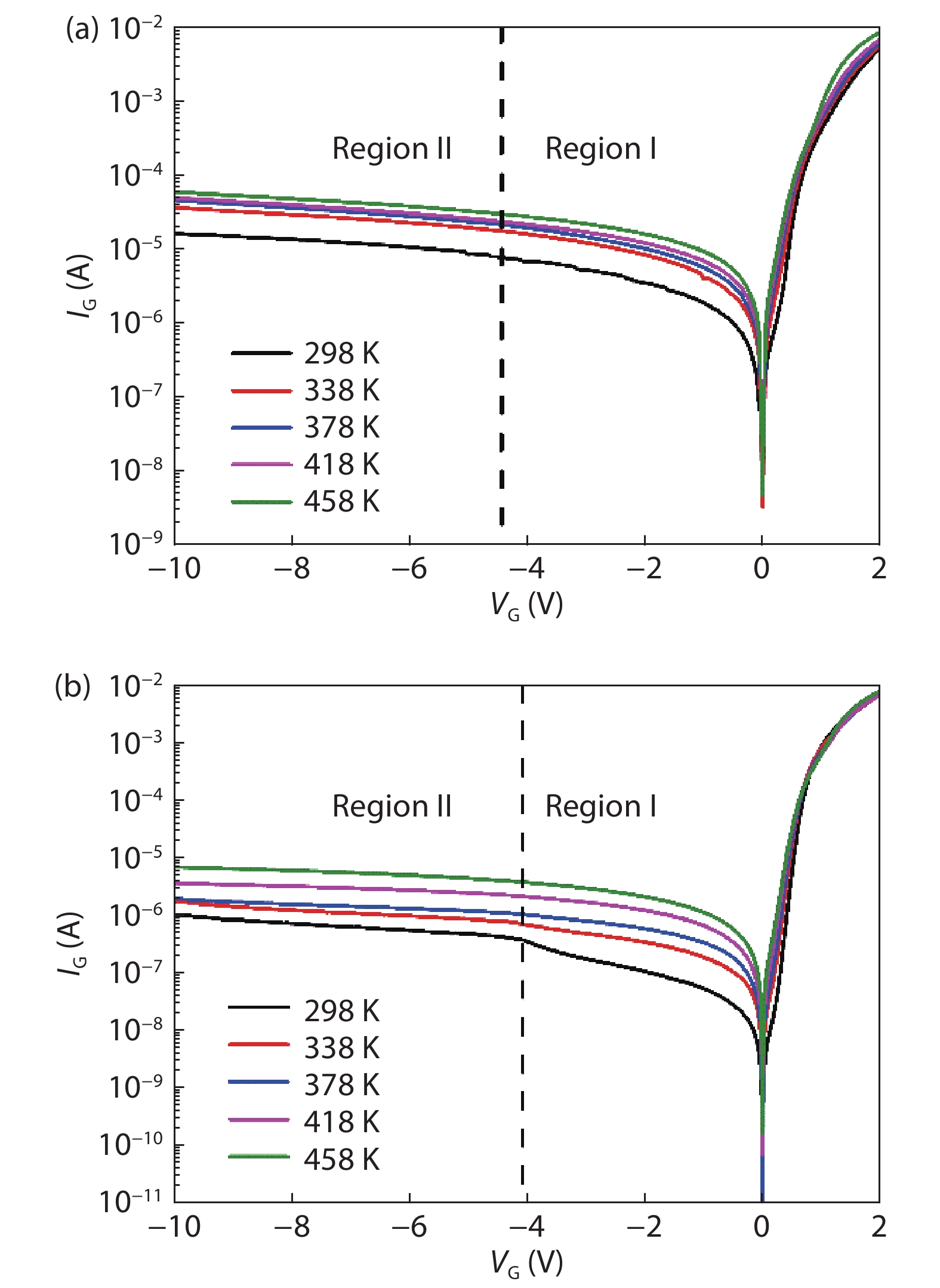
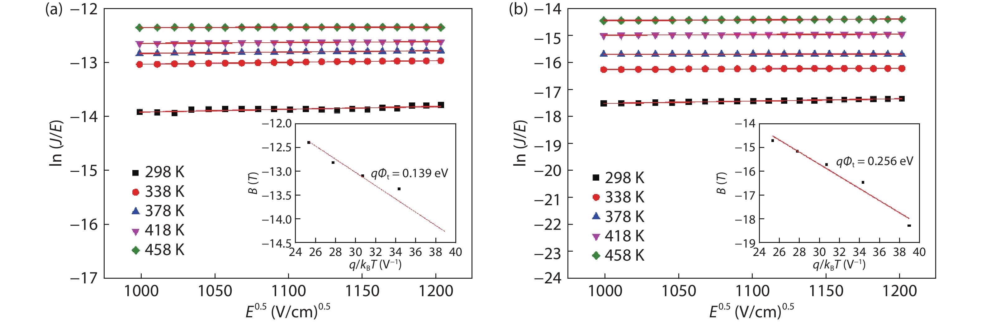
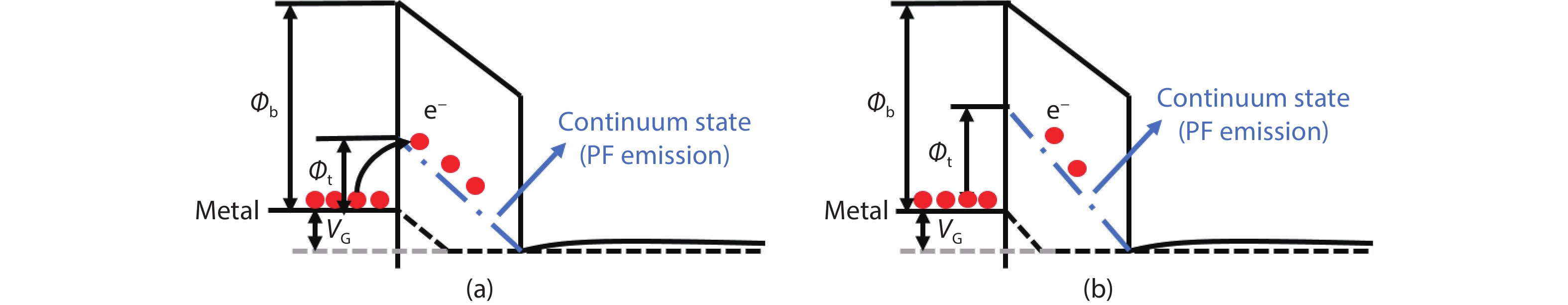
Abstract: In this paper, we investigated the effect of post-gate annealing (PGA) on reverse gate leakage and the reverse bias reliability of Al0.23Ga0.77N/GaN high electron mobility transistors (HEMTs). We found that the Poole–Frenkel (PF) emission is dominant in the reverse gate leakage current at the low reverse bias region (Vth < VG < 0 V) for the unannealed and annealed HEMTs. The emission barrier height of HEMT is increased from 0.139 to 0.256 eV after the PGA process, which results in a reduction of the reverse leakage current by more than one order. Besides, the reverse step stress was conducted to study the gate reliability of both HEMTs. After the stress, the unannealed HEMT shows a higher reverse leakage current due to the permanent damage of the Schottky gate. In contrast, the annealed HEMT shows a little change in reverse leakage current. This indicates that the PGA can reduce the reverse gate leakage and improve the gate reliability.
Key words: AlGaN/GaN HEMTs, gate leakage, PF emission, post-gate annealing (PGA)
| [1] |
Wu S, Ma X H, Yang L, et al. A millimeter-wave AlGaN/GaN HEMT fabricated with transitional-recessed-gate technology for high-gain and high-linearity applications. IEEE Electron Device Lett, 2019, 40, 846 doi: 10.1109/LED.2019.2909770
|
| [2] |
Moon J S, Wong J, Grabar B, et al. 360 GHz fMAX graded-channel AlGaN/GaN HEMTs for mmW low-noise applications. IEEE Electron Device Lett, 2020, 41, 1173 doi: 10.1109/LED.2020.3005337
|
| [3] |
Murugapandiyan P, Ravimaran S, William J, et al. Design and analysis of 30 nm T-gate InAlN/GaN HEMT with AlGaN back-barrier for high power microwave applications. Superlattices Microstruct, 2017, 111, 1050 doi: 10.1016/j.spmi.2017.08.002
|
| [4] |
Chen Y Q, Liao X Y, Zeng C, et al. Degradation mechanism of AlGaN/GaN HEMTs during high temperature operation stress. Semicond Sci Technol, 2018, 33, 015019 doi: 10.1088/1361-6641/aa9d71
|
| [5] |
del Alamo J A, Joh J. GaN HEMT reliability. Microelectron Reliab, 2009, 49, 1200 doi: 10.1016/j.microrel.2009.07.003
|
| [6] |
Gao Z, Rampazzo F, Meneghini M, et al. Degradation mechanism of 0.15 μm AlGaN/GaN HEMTs: Effects of hot electrons. Microelectron Reliab, 2020, 114, 113905 doi: 10.1016/j.microrel.2020.113905
|
| [7] |
Marcon D, Kauerauf T, Medjdoub F, et al. A comprehensive reliability investigation of the voltage-, temperature- and device geometry-dependence of the gate degradation on state-of-the-art GaN-on-Si HEMTs. 2010 International Electron Devices Meeting, 2010, 20.3.1
|
| [8] |
Sudharsanan S, Karmalkar S. Modeling of the reverse gate leakage in AlGaN/GaN high electron mobility transistors. J Appl Phys, 2010, 107, 064501 doi: 10.1063/1.3340826
|
| [9] |
Jos R. Reverse Schottky gate current in AlGaN-GaN high-electron-mobility-transistors. J Appl Phys, 2012, 112, 094508 doi: 10.1063/1.4764866
|
| [10] |
Zhang H, Miller E J, Yu E T. Analysis of leakage current mechanisms in Schottky contacts to GaN and Al0.25Ga0.75N∕GaN grown by molecular-beam epitaxy. J Appl Phys, 2006, 99, 023703 doi: 10.1063/1.2159547
|
| [11] |
Turuvekere S, Rawal D S, DasGupta A, et al. Evidence of Fowler–Nordheim tunneling in gate leakage current of AlGaN/ GaN HEMTs at room temperature. IEEE Trans Electron Devices, 2014, 61, 4291 doi: 10.1109/TED.2014.2361436
|
| [12] |
Kotani J, Tajima M, Kasai S, et al. Mechanism of surface conduction in the vicinity of Schottky gates on AlGaN∕GaN heterostructures. Appl Phys Lett, 2007, 91, 093501 doi: 10.1063/1.2775834
|
| [13] |
Zhang S, Liu X Y, Wei K, et al. Suppression of gate leakage current in ka-band AlGaN/GaN HEMT with 5-nm SiN gate dielectric grown by plasma-enhanced ALD. IEEE Trans Electron Devices, 2021, 68, 49 doi: 10.1109/TED.2020.3037888
|
| [14] |
Kim K, Kim T J, Zhang H L, et al. AlGaN/GaN Schottky-gate HEMTs with UV/O3-treated gate interface. IEEE Electron Device Lett, 2020, 41, 1488 doi: 10.1109/LED.2020.3019339
|
| [15] |
Liu L, Xi Y Y, Ahn S, et al. Characteristics of gate leakage current and breakdown voltage of AlGaN/GaN high electron mobility transistors after postprocess annealing. J Vac Sci Technol B, 2014, 32, 052201 doi: 10.1116/1.4891168
|
| [16] |
Kim H, Lee J, Liu D M, et al. Gate current leakage and breakdown mechanism in unpassivated AlGaN∕GaN high electron mobility transistors by post-gate annealing. Appl Phys Lett, 2005, 86, 143505 doi: 10.1063/1.1899255
|
| [17] |
Sleptsov E V, Chernykh A V, Chernykh S V, et al. Investigation of the thermal annealing effect on electrical properties of Ni/Au, Ni/Mo/Au and Mo/Au Schottky barriers on AlGaN/GaN heterostructures. J Phys: Conf Ser, 2017, 816, 012039 doi: 10.1088/1742-6596/816/1/012039
|
| [18] |
Visvkarma A K, Laishram R, Kapoor S, et al. Improvement in DC and pulse characteristics of AlGaN/GaN HEMT by employing dual metal gate structure. Semicond Sci Technol, 2019, 34, 105013 doi: 10.1088/1361-6641/ab3ce4
|
| [19] |
Yan D W, Lu H, Cao D S, et al. On the reverse gate leakage current of AlGaN/GaN high electron mobility transistors. Appl Phys Lett, 2010, 97, 153503 doi: 10.1063/1.3499364
|
| [20] |
Hao M L, Wang Q, Jiang L J, et al. Gate leakage and breakdown characteristics of AlGaN/GaN high-electron-mobility transistors with Fe delta-doped buffer. Nanosci Nanotechnol Lett, 2018, 10, 185 doi: 10.1166/nnl.2018.2601
|
| [21] |
Lin Z J, Kim H, Lee J, et al. Thermal stability of Schottky contacts on strained AlGaN/GaN heterostructures. Appl Phys Lett, 2004, 84, 1585 doi: 10.1063/1.1650875
|
| [22] |
Turuvekere S, Karumuri N, Rahman A A, et al. Gate leakage mechanisms In AlGaN/GaN and AlInN/GaN HEMTs: Comparison and modeling. IEEE Trans Electron Devices, 2013, 60, 3157 doi: 10.1109/TED.2013.2272700
|
| [23] |
Kim H, Schuette M L, Lee J, et al. Passivation of surface and interface states in AlGaN/GaN HEMT structures by annealing. J Electron Mater, 2007, 36, 1149 doi: 10.1007/s11664-007-0189-2
|
| [24] |
Marcon D, Viaene J, Favia P, et al. Reliability of AlGaN/GaN HEMTs: Permanent leakage current increase and output current drop. Proceedings of the 20th IEEE International Symposium on the Physical and Failure Analysis of Integrated Circuits (IPFA), 2013, 249
|
| [25] |
Chang C Y, Douglas E A, Kim J, et al. Electric-field-driven degradation in off-state step-stressed AlGaN/GaN high-electron mobility transistors. IEEE Trans Device Mater Reliab, 2011, 11, 187 doi: 10.1109/TDMR.2010.2103314
|
| [26] |
Meneghini M, Stocco A, Bertin M, et al. Time-dependent degradation of AlGaN/GaN high electron mobility transistors under reverse bias. Appl Phys Lett, 2012, 100, 033505 doi: 10.1063/1.3678041
|


Article views: 3021 Times PDF downloads: 159 Times Cited by: 0 Times
Received: 01 April 2021 Revised: 16 April 2021 Online: Accepted Manuscript: 04 June 2021Uncorrected proof: 09 June 2021Published: 01 September 2021
| Citation: |
Changxi Chen, Quan Wang, Wei Li, Qian Wang, Chun Feng, Lijuan Jiang, Hongling Xiao, Xiaoliang Wang. Effect of the post-gate annealing on the gate reliability of AlGaN/GaN HEMTs[J]. Journal of Semiconductors, 2021, 42(9): 092802. doi: 10.1088/1674-4926/42/9/092802
C X Chen, Q Wang, W Li, Q Wang, C Feng, L J Jiang, H L Xiao, X L Wang, Effect of the post-gate annealing on the gate reliability of AlGaN/GaN HEMTs[J]. J. Semicond., 2021, 42(9): 092802. doi: 10.1088/1674-4926/42/9/092802.
Export: BibTex EndNote

|
| [1] |
Wu S, Ma X H, Yang L, et al. A millimeter-wave AlGaN/GaN HEMT fabricated with transitional-recessed-gate technology for high-gain and high-linearity applications. IEEE Electron Device Lett, 2019, 40, 846 doi: 10.1109/LED.2019.2909770
|
| [2] |
Moon J S, Wong J, Grabar B, et al. 360 GHz fMAX graded-channel AlGaN/GaN HEMTs for mmW low-noise applications. IEEE Electron Device Lett, 2020, 41, 1173 doi: 10.1109/LED.2020.3005337
|
| [3] |
Murugapandiyan P, Ravimaran S, William J, et al. Design and analysis of 30 nm T-gate InAlN/GaN HEMT with AlGaN back-barrier for high power microwave applications. Superlattices Microstruct, 2017, 111, 1050 doi: 10.1016/j.spmi.2017.08.002
|
| [4] |
Chen Y Q, Liao X Y, Zeng C, et al. Degradation mechanism of AlGaN/GaN HEMTs during high temperature operation stress. Semicond Sci Technol, 2018, 33, 015019 doi: 10.1088/1361-6641/aa9d71
|
| [5] |
del Alamo J A, Joh J. GaN HEMT reliability. Microelectron Reliab, 2009, 49, 1200 doi: 10.1016/j.microrel.2009.07.003
|
| [6] |
Gao Z, Rampazzo F, Meneghini M, et al. Degradation mechanism of 0.15 μm AlGaN/GaN HEMTs: Effects of hot electrons. Microelectron Reliab, 2020, 114, 113905 doi: 10.1016/j.microrel.2020.113905
|
| [7] |
Marcon D, Kauerauf T, Medjdoub F, et al. A comprehensive reliability investigation of the voltage-, temperature- and device geometry-dependence of the gate degradation on state-of-the-art GaN-on-Si HEMTs. 2010 International Electron Devices Meeting, 2010, 20.3.1
|
| [8] |
Sudharsanan S, Karmalkar S. Modeling of the reverse gate leakage in AlGaN/GaN high electron mobility transistors. J Appl Phys, 2010, 107, 064501 doi: 10.1063/1.3340826
|
| [9] |
Jos R. Reverse Schottky gate current in AlGaN-GaN high-electron-mobility-transistors. J Appl Phys, 2012, 112, 094508 doi: 10.1063/1.4764866
|
| [10] |
Zhang H, Miller E J, Yu E T. Analysis of leakage current mechanisms in Schottky contacts to GaN and Al0.25Ga0.75N∕GaN grown by molecular-beam epitaxy. J Appl Phys, 2006, 99, 023703 doi: 10.1063/1.2159547
|
| [11] |
Turuvekere S, Rawal D S, DasGupta A, et al. Evidence of Fowler–Nordheim tunneling in gate leakage current of AlGaN/ GaN HEMTs at room temperature. IEEE Trans Electron Devices, 2014, 61, 4291 doi: 10.1109/TED.2014.2361436
|
| [12] |
Kotani J, Tajima M, Kasai S, et al. Mechanism of surface conduction in the vicinity of Schottky gates on AlGaN∕GaN heterostructures. Appl Phys Lett, 2007, 91, 093501 doi: 10.1063/1.2775834
|
| [13] |
Zhang S, Liu X Y, Wei K, et al. Suppression of gate leakage current in ka-band AlGaN/GaN HEMT with 5-nm SiN gate dielectric grown by plasma-enhanced ALD. IEEE Trans Electron Devices, 2021, 68, 49 doi: 10.1109/TED.2020.3037888
|
| [14] |
Kim K, Kim T J, Zhang H L, et al. AlGaN/GaN Schottky-gate HEMTs with UV/O3-treated gate interface. IEEE Electron Device Lett, 2020, 41, 1488 doi: 10.1109/LED.2020.3019339
|
| [15] |
Liu L, Xi Y Y, Ahn S, et al. Characteristics of gate leakage current and breakdown voltage of AlGaN/GaN high electron mobility transistors after postprocess annealing. J Vac Sci Technol B, 2014, 32, 052201 doi: 10.1116/1.4891168
|
| [16] |
Kim H, Lee J, Liu D M, et al. Gate current leakage and breakdown mechanism in unpassivated AlGaN∕GaN high electron mobility transistors by post-gate annealing. Appl Phys Lett, 2005, 86, 143505 doi: 10.1063/1.1899255
|
| [17] |
Sleptsov E V, Chernykh A V, Chernykh S V, et al. Investigation of the thermal annealing effect on electrical properties of Ni/Au, Ni/Mo/Au and Mo/Au Schottky barriers on AlGaN/GaN heterostructures. J Phys: Conf Ser, 2017, 816, 012039 doi: 10.1088/1742-6596/816/1/012039
|
| [18] |
Visvkarma A K, Laishram R, Kapoor S, et al. Improvement in DC and pulse characteristics of AlGaN/GaN HEMT by employing dual metal gate structure. Semicond Sci Technol, 2019, 34, 105013 doi: 10.1088/1361-6641/ab3ce4
|
| [19] |
Yan D W, Lu H, Cao D S, et al. On the reverse gate leakage current of AlGaN/GaN high electron mobility transistors. Appl Phys Lett, 2010, 97, 153503 doi: 10.1063/1.3499364
|
| [20] |
Hao M L, Wang Q, Jiang L J, et al. Gate leakage and breakdown characteristics of AlGaN/GaN high-electron-mobility transistors with Fe delta-doped buffer. Nanosci Nanotechnol Lett, 2018, 10, 185 doi: 10.1166/nnl.2018.2601
|
| [21] |
Lin Z J, Kim H, Lee J, et al. Thermal stability of Schottky contacts on strained AlGaN/GaN heterostructures. Appl Phys Lett, 2004, 84, 1585 doi: 10.1063/1.1650875
|
| [22] |
Turuvekere S, Karumuri N, Rahman A A, et al. Gate leakage mechanisms In AlGaN/GaN and AlInN/GaN HEMTs: Comparison and modeling. IEEE Trans Electron Devices, 2013, 60, 3157 doi: 10.1109/TED.2013.2272700
|
| [23] |
Kim H, Schuette M L, Lee J, et al. Passivation of surface and interface states in AlGaN/GaN HEMT structures by annealing. J Electron Mater, 2007, 36, 1149 doi: 10.1007/s11664-007-0189-2
|
| [24] |
Marcon D, Viaene J, Favia P, et al. Reliability of AlGaN/GaN HEMTs: Permanent leakage current increase and output current drop. Proceedings of the 20th IEEE International Symposium on the Physical and Failure Analysis of Integrated Circuits (IPFA), 2013, 249
|
| [25] |
Chang C Y, Douglas E A, Kim J, et al. Electric-field-driven degradation in off-state step-stressed AlGaN/GaN high-electron mobility transistors. IEEE Trans Device Mater Reliab, 2011, 11, 187 doi: 10.1109/TDMR.2010.2103314
|
| [26] |
Meneghini M, Stocco A, Bertin M, et al. Time-dependent degradation of AlGaN/GaN high electron mobility transistors under reverse bias. Appl Phys Lett, 2012, 100, 033505 doi: 10.1063/1.3678041
|

 WeChat ID
Journal of Semiconductors © 2017 All Rights Reserved 京ICP备05085259号-2

 DownLoad:

