| [1] |
Huang R, Tao Y, Bai S, et al. Design and fabrication of a 3.3 kV 4H-SiC MOSFET. J Semiconduct, 2015, 36, 094002 doi: 10.1088/1674-4926/36/9/094002 |
| [2] |
Chatterjee A, Stevenson P, Franceschi S D, et al. Semiconductor qubits in practice. Nat Rev Phys, 2021, 3, 157 doi: 10.1038/s42254-021-00283-9 |
| [3] |
Gao F, Weber W J. Mechanical properties and elastic constants due to damage accumulation and amorphization in SiC. Phys Rev B, 2004, 69, 224108 doi: 10.1103/PhysRevB.69.224108 |
| [4] |
Liu X, Zhang J, Xu B, et al. Deformation of 4H-SiC: the role of dopants. Appl Phys Lett, 2022, 120, 052105 doi: 10.1063/5.0083882 |
| [5] |
Wang W, Zhang B, Shi Y, et al. Improvement in chemical mechanical polishing of 4H-SiC wafer by activating persulfate through the synergistic effect of UV and TiO 2. J Mater Process Tech, 2021, 295, 117150 doi: 10.1016/j.jmatprotec.2021.117150 |
| [6] |
Sasaki M, Tamura K, Sako H, et al. Analysis on generation of localized step-bunchings on 4H-SiC(0001) Si face by synchrotron X-ray topography. Mater Sci Forum, 2014, 778–780, 398 doi: 10.4028/www.scientific.net/MSF.778-780.398 |
| [7] |
Sasaki M, Matsuhata H, Tamura K, et al. Synchrotron X-Ray topography analysis of local damage occurring during polishing of 4H-SiC wafers. Jpn J Appl Phys, 2015, 54, 091301 doi: 10.7567/JJAP.54.091301 |
| [8] |
Zhang Z, Cai H, Gan D, et al. A new method to characterize underlying scratches on SiC wafers. CrystEngComm, 2019, 21, 1200 doi: 10.1039/C8CE01700J |
| [9] |
Zhang Y, Zhang L, Chen K, et al. Rapid subsurface damage detection of SiC using inductivity coupled plasma. Int J Extrem Manuf, 2021, 3, 035202 doi: 10.1088/2631-7990/abff34 |
| [10] |
Dudley M, Zhang N, Zhang Y, et al. Nucleation of c-axis screw dislocations at substrate surface damage during 4H-silicon carbide homo-epitaxy. Mater Sci Forum, 2010, 645–648, 295 doi: 10.4028/www.scientific.net/MSF.645-648.295 |
| [11] |
Ashida K, Dojima D, Torimi S, et al. Rearrangement of surface structure of 4° off-axis 4H-SiC (0001) epitaxial wafer by high temperature annealing in Si/Ar ambient. Mater Sci Forum, 2018, 924, 249 doi: 10.4028/www.scientific.net/MSF.924.249 |
| [12] |
Ashida K, Dojima D, Kutsuma Y, et al. Evaluation of polishing-induced subsurface damage of 4H-SiC (0001) by cross-sectional electron backscattered diffraction and synchrotron x-ray micro-diffraction. MRS Adv, 2016, 1, 3697 doi: 10.1557/adv.2016.433 |
| [13] |
Sako H, Matsuhata H, Sasaki M, et al. Micro-structural analysis of local damage introduced in subsurface regions of 4H-SiC wafers during chemo-mechanical polishing. J Appl Phys, 2016, 119, 135702 doi: 10.1063/1.4945017 |
| [14] |
Xu Z, He Z, Song Y, et al. Topic review: application of Raman spectroscopy characterization in micro/nano-machining. Micromachines, 2018, 9, 361 doi: 10.3390/mi9070361 |
| [15] |
Li H, Cui C, Bian S, et al. Double-sided and single-sided polished 6H-SiC wafers with subsurface damage layer studied by Mueller matrix ellipsometry. J Appl Phys, 2020, 128, 235304 doi: 10.1063/5.0026124 |
| [16] |
Yin J, Bai Q, Zhang B. Methods for detection of subsurface damage: a review. Chin J Mech Eng, 2018, 31, 41 doi: 10.1186/s10033-018-0229-2 |
| [17] |
Wu L, Yu B, Zhang P, et al. Rapid identification of ultrathin amorphous damage on monocrystalline silicon surface. Phys Chem Chem Phys, 2020, 22, 12987 doi: 10.1039/D0CP01370F |
| [18] |
|
| [19] |
Zhou P, Xu S, Wang Z, et al. A load identification method for the grinding damage induced stress (GDIS) distribution in silicon wafers. Int J Mach Tools Manuf, 2016, 107, 1 doi: 10.1016/j.ijmachtools.2016.04.010 |
| [20] |
Sekhar H, Fukuda T, Kida Y, et al. The impact of damage etching on fracture strength of diamond wire sawn monocrystalline silicon wafers for photovoltaics use. Jpn J Appl Phys, 2018, 57, 126501 doi: 10.7567/JJAP.57.126501 |
| [21] |
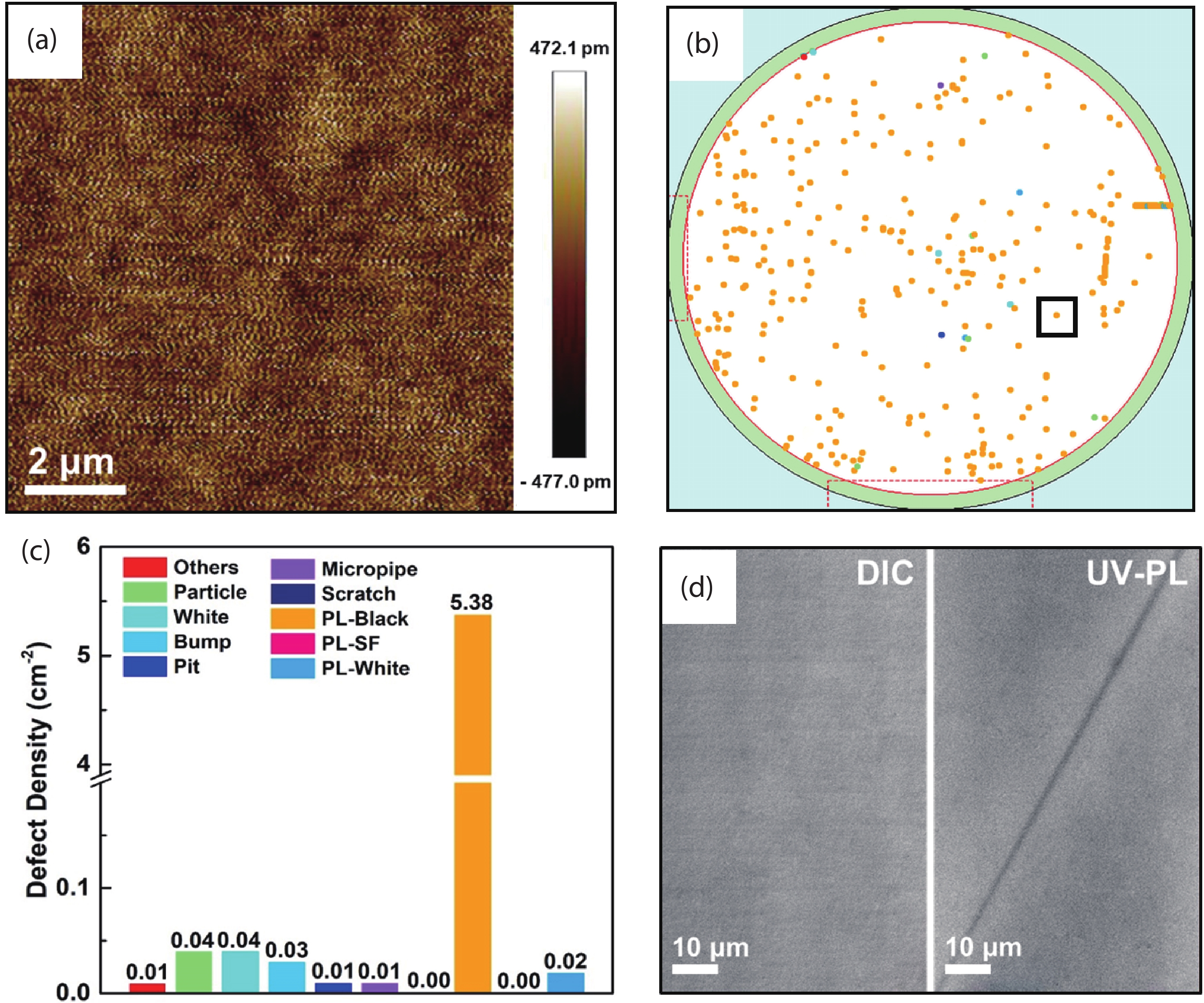
Luo H, Li J, Yang G, et al. Electronic and optical properties of threading dislocations in n-type 4H-SiC. ACS Appl Electron Mater, 2022, 4, 1678 doi: 10.1021/acsaelm.1c01330 |
| [22] |
Liu J, Liu J, Liu C, et al. 3D dark-field confocal microscopy for subsurface defects detection. Opt Lett, 2020, 45(3), 660 doi: 10.1364/OL.384487 |
| [23] |
Youtsey C, Romano L T, Adesida I. Gallium nitride whiskers formed by selective photoenhanced wet etching of dislocations. Appl Phys Lett, 1998, 73(6), 10 doi: 10.1063/1.122005 |
| [24] |
Weyher J L, van Dorp D H, Kelly J J. Principles of electroless photoetching of non-uniformly doped GaN: kinetics and defect revealing. J Cryst Growth, 2015, 430, 21 doi: 10.1016/j.jcrysgro.2015.08.003 |
| [25] |
Lazar S, Weyher J L, Macht L, et al. Nanopipes in GaN: photo-etching and TEM study. Eur Phys J Appl Phys, 2004, 27, 275 doi: 10.1051/epjap:2004047 |
| [26] |
Weyher J L, Lazar S, Borysiuk J, et al. Defect-selective etching of SiC. Phys Stat Sol A, 2005, 202(4), 578 doi: 10.1002/pssa.200460432 |
| [27] |
Weyher J L. Defect sensitive etching of nitrides: appraisal of methods. Cryst Res Technol, 2012, 47(3), 333 doi: 10.1002/crat.201100421 |
| [28] |
Weyher J L, Smalc-Koziorowska J, Bańkowska M, et al. Photo-etching of GaN: revealing nano-scale non-homogeneities. J Cryst Growth, 2015, 426, 153 doi: 10.1016/j.jcrysgro.2015.05.031 |
| [29] |
Macht L, Kelly J J, Weyher J L, et al. An electrochemical study of photoetching of heteroepitaxial GaN: kinetics and morphology. J Cryst Growth, 2005, 273, 347 doi: 10.1016/j.jcrysgro.2004.09.029 |
| [30] |
Van Dorp D H, Weyher J L, Kelly J J. Anodic etching of SiC in alkaline solutions. J Micromech Microeng, 2007, 17, 50 doi: 10.1088/0960-1317/17/1/007 |
| [31] |
Harima H, Nakashima S, Uemura T. Raman scattering from anisotropic LO-phonon-plasmon-coupled mode in n-type 4H- and 6H-SiC. J Appl Phys, 1995, 78, 1996 doi: 10.1063/1.360174 |
| [32] |
Mahadik N A, Stahlbush R E, Qadri S B, et al. Structure and morphology of inclusions in 4 offcut 4H-SiC epitaxial layers. J Electron Mater, 2011, 40(4), 413 doi: 10.1007/s11664-011-1570-8 |
| [33] |
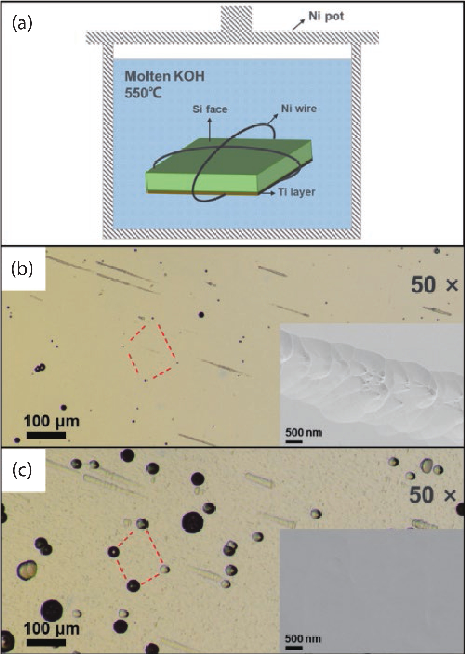
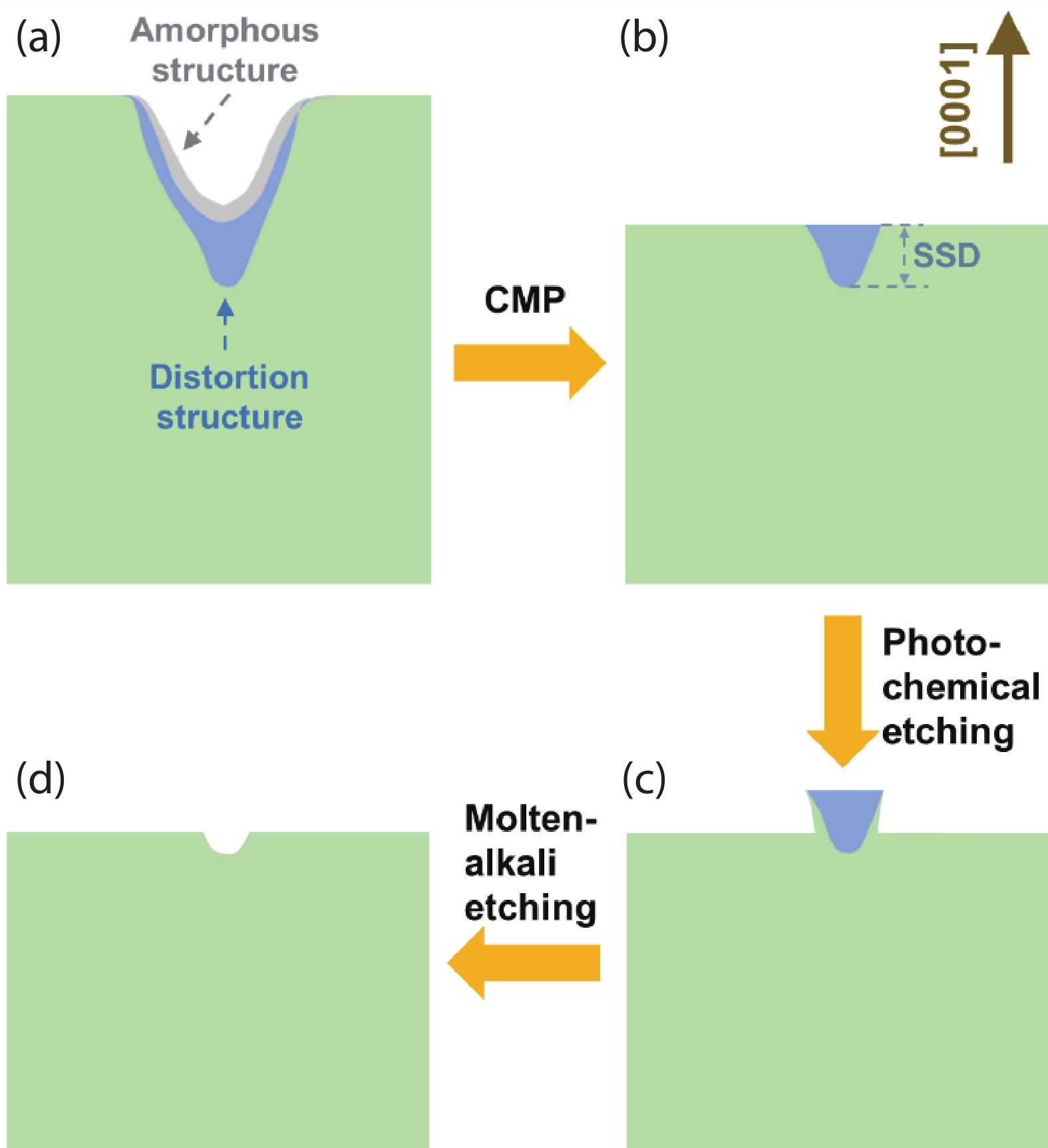
Katsuno M, Ohtani N, Takahashi J, et al. Mechanism of molten KOH etching of SiC single crystals: comparative study with thermal oxidation. Jpn J Appl Phys, 1999, 38, 4661 doi: 10.1143/JJAP.38.4661 |
| [34] |
Gao Y, Zhang Z, Bondokov R, et al. The effect of doping concentration and conductivity type on preferential etching of 4H-SiC by molten KOH. MRS Online Proceedings Library, 2004, 815, 6
|
| [35] |
Zhu B, Zhao D, Zhao H. A study of deformation behavior and phase transformation in 4H-SiC during nanoindentation process via molecular dynamics simulation. Ceram Int, 2019, 45, 5150 doi: 10.1016/j.ceramint.2018.10.261 |


 DownLoad: