ARTICLES

Effect of charge trapping on electrical characteristics of silicon junctionless nanowire transistor

Yifan Fu1, Liuhong Ma1, 2, 3, , Zhiyong Duan1, 4 and Weihua Han2, 3,

+ Author Affiliations

 Corresponding author: Liuhong Ma, Email: maliuhong@zzu.edu.cn; Weihua Han, Email: weihua@semi.ac.cn

PDF

Turn off MathJax

Abstract: We investigated the effect of charge trapping on electrical characteristics of silicon junctionless nanowire transistors which are fabricated on heavily n-type doped silicon-on-insulator substrate. The obvious random telegraph noise and current hysteresis observed at the temperature of 10 K indicate the existence of acceptor-like traps. The position depth of the traps in the oxide from Si/SiO2 interface is 0.35 nm, calculated by utilizing the dependence of the capture and emission time on the gate voltage. Moreover, by constructing a three-dimensional model of tri-gate device structure in COMSOL Multiphysics simulation software, we achieved the trap density of 1.9 × 1012 cm–2 and the energy level position of traps at 0.18 eV below the intrinsic Fermi level.

Key words: junctionless transistorcharge trappingrandom telegraph signals


[1]
Zhou W H, Zhang S L, Guo S Y, et al. Designing sub-10-nm metal-oxide-semiconductor field-effect transistors via ballistic transport and disparate effective mass: The case of two-dimensional BiN. Phys Rev Appl, 2020, 13(4), 044066 doi: 10.1103/PhysRevApplied.13.044066
[2]
Zhou W H, Zhang S L, Wang Y Y. Anisotropic in-plane ballistic transport in monolayer black arsenic-phosphorus FETs. Adv Electron Mater, 2020, 6(3), 1901281 doi: 10.1002/aelm.201901281
[3]
Jeon D Y, Mouis M, Barraud S, et al. Channel width dependent subthreshold operation of tri-gate junctionless transistors. Solid-State Electron, 2020, 171, 107860 doi: 10.1016/j.sse.2020.107860
[4]
Colinge J P, Lee C W, Afzalian A, et al. Nanowire transistors without junctions. Nat Nanotechnol, 2010, 5, 225 doi: 10.1038/nnano.2010.15
[5]
Mendiratta N, Tripathi S L. A review on performance comparison of advanced MOSFET structures below 45 nm technology node. J Semicond, 2020, 41(6), 061401 doi: 10.1088/1674-4926/41/6/061401
[6]
Lee J, Kim Y, Cho S. Design of poly-Si junctionless Fin-channel FET with quantum-mechanical drift-diffusion models for sub-10-nm technology nodes. IEEE Trans Electron Dev, 2016, 63, 4610 doi: 10.1109/TED.2016.2614990
[7]
Yan R, Kranti A, Ferain I, et al. Investigation of high-performance sub-50 nm junctionless nanowire transistors. Microelectron Reliab, 2011, 51(7), 1166 doi: 10.1016/j.microrel.2011.02.016
[8]
Rudenko T, Nazarov A, Ferain I, et al. Mobility enhancement effect in heavily doped junctionless nanowire silicon-on-insulator metal-oxide-semiconductor field-effect transistors. Appl Phys Lett, 2012, 101, 053511 doi: 10.1063/1.4767353
[9]
Gupta S, Nigam K, Pandey S, et al. Effect of interface trap charges on performance variation of heterogeneous gate dielectric junctionless-TFET. IEEE Trans Electron Dev, 2017, 64(11), 1 doi: 10.1109/TED.2017.2754297
[10]
Nazarov A N, Ferain I, Akhavan N D, et al. Random telegraph-signal noise in junctionless transistors. Appl Phys Lett, 2011, 98(9), 092111 doi: 10.1063/1.3557505
[11]
Berengue O M, Chiquito J. Direct evidence of traps controlling the carriers transport in SnO2 nanobelts. J Semicond, 2017, 38(12), 122001 doi: 10.1088/1674-4926/38/12/122001
[12]
Ma L H, Han W H, Wang H, et al. Charge trapping in surface accumulation layer of heavily doped junctionless nanowire transistors. Chin Phys B, 2015, 024(012), 589 doi: 10.1088/1674-1056/24/12/128101
[13]
Hu G X, Hu S Y, Feng J H, et al. Analytical models for channel potential, threshold voltage, and subthreshold swing of junctionless triple-gate FinFETs. Microelectron J, 2016, 50, 60 doi: 10.1016/j.mejo.2016.02.003
[14]
Liu F Y, Liu H Z, Liu B W, et al. An analytical model for nanowire junctionless SOI FinFETs with considering three-dimensional coupling effect. Chin Phys B, 2016, 25(4), 047305 doi: 10.1088/1674-1056/25/4/047305
[15]
Ávila-Herreraa F, Pazb B C, Cerdeira A. Charge-based compact analytical model for triple-gate junctionless nanowire transistors. Solid-State Electron, 2016, 122(1), 23 doi: 10.1016/j.sse.2016.04.013
[16]
Liang Y Y, Jang Kyungsoo, Velumani S, et al. Effects of interface trap density on the electrical performance of amorphous InSnZnO thin-film transistor. J Semicond, 2015, 36(2), 024007 doi: 10.1088/1674-4926/36/2/024007
[17]
Liu F, Wang K L, Li C, et al. Study of random telegraph signals in single-walled carbon nanotube field effect transistors. IEEE Trans Nanotechnol, 2006, 5(5), 441 doi: 10.1109/TNANO.2006.880906
[18]
Sun Y, Zhang L N, Ahmed Z, et al. Characterization of interface trap dynamics responsible for hysteresis in organic thin-film transistors. Org Electron, 2015, 27, 192 doi: 10.1016/j.orgel.2015.09.011
[19]
Amarasinghe N V, Elik-Butler Z, Vasina P, et al. Characterization of oxide traps in 0.15 μm2 MOSFETs using random telegraph signals. Microelectron Reliab, 2000, 40(11), 1875 doi: 10.1016/S0026-2714(00)00089-5
[20]
Celik-Butler Z, Vasina P. A method for locating the position of oxide traps responsible for random telegraph signals in submicron MOSFETs. IEEE Trans Electron Dev, 2000, 47(3), 646 doi: 10.1109/16.824742
[21]
Cheng Y C, Chen H B, Han M H, et al. Temperature dependence of electronic behaviors in quantum dimension junctionless thin-film transistor. Nanoscale Res Lett, 2014, 9(1), 1 doi: 10.1186/1556-276X-9-392
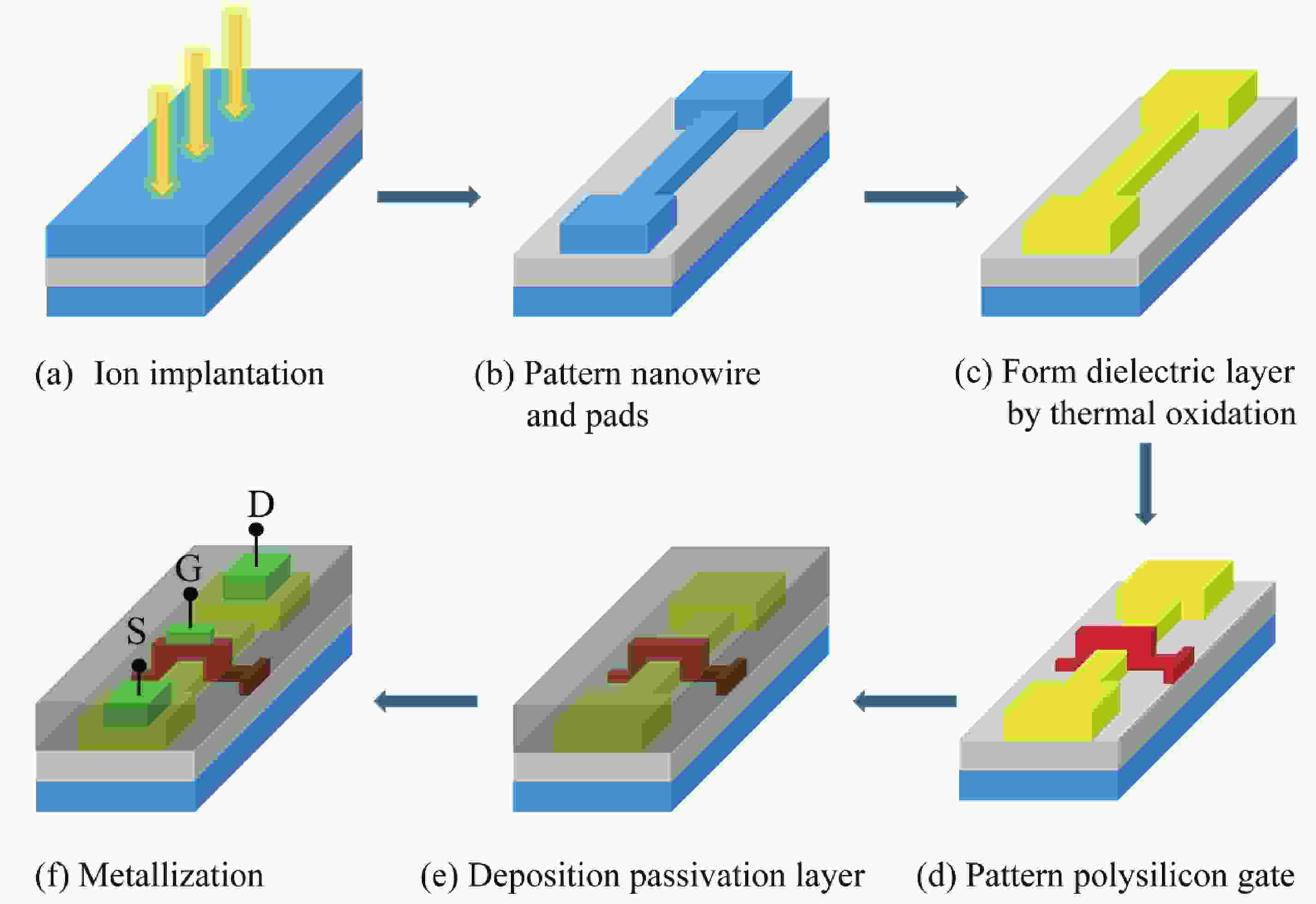
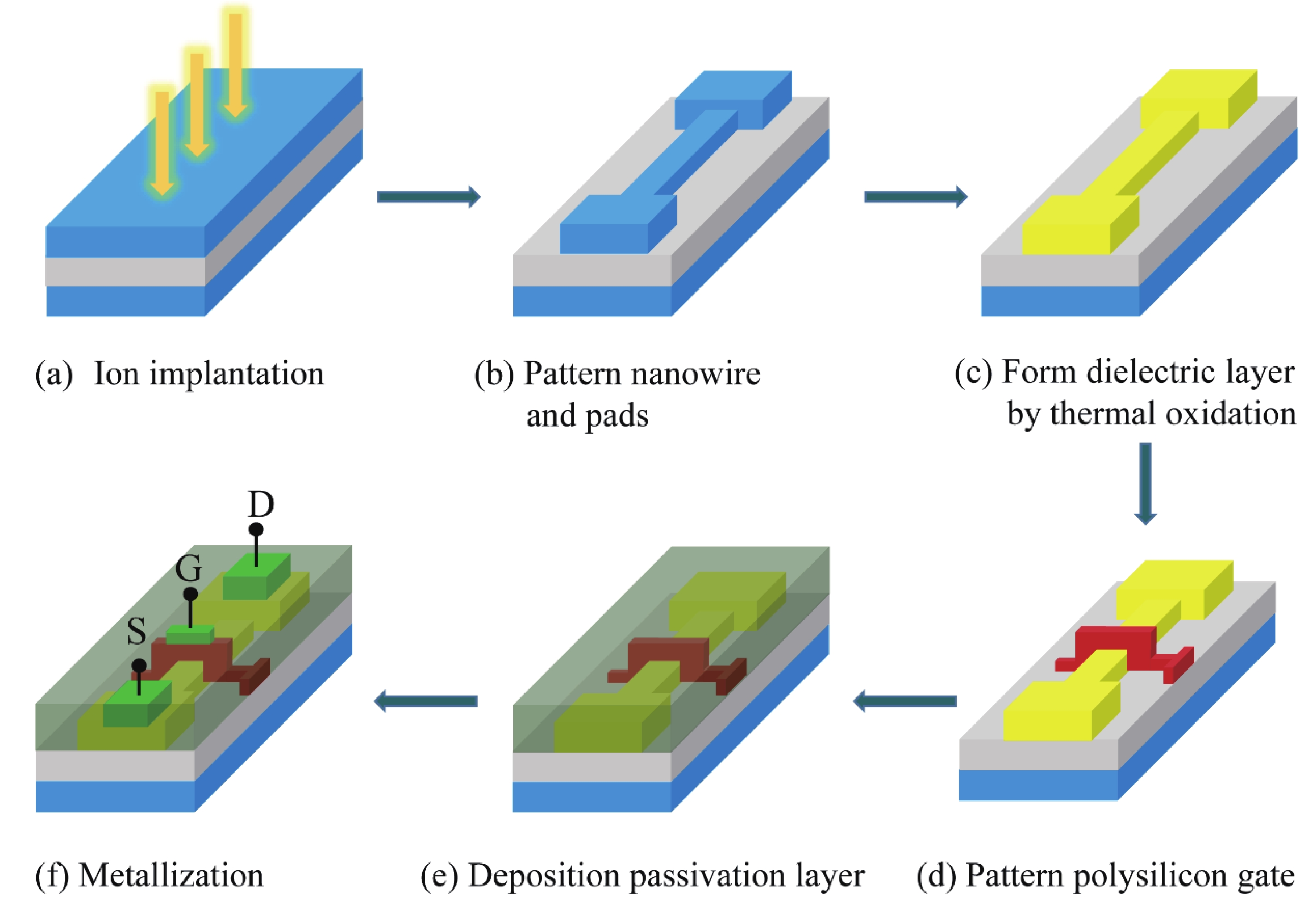
Fig. 1.  (Color online) Schematic diagrams of the fabrication process for JNTs.

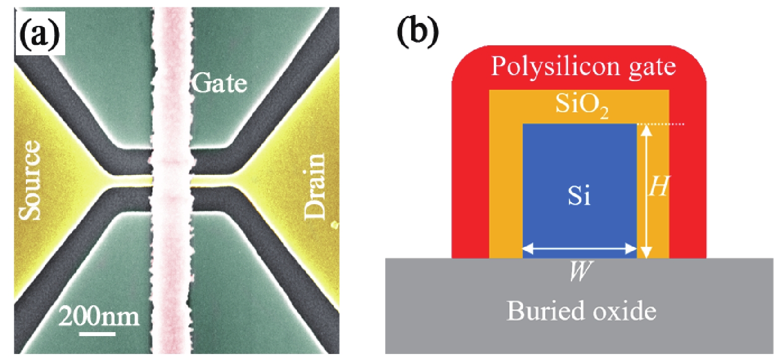
Fig. 2.  (Color online) (a) The color SEM image of devices with the gate length of 280 nm. (b) The cross-section schematics of the devices.

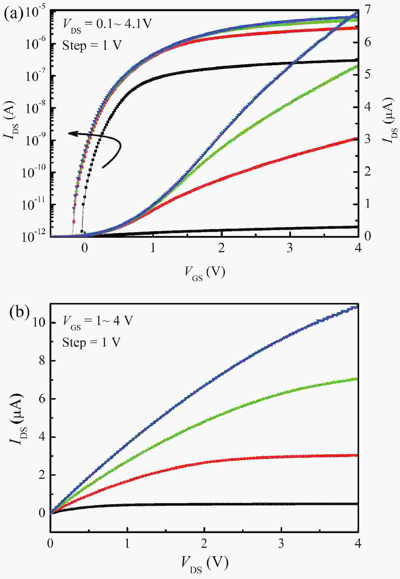
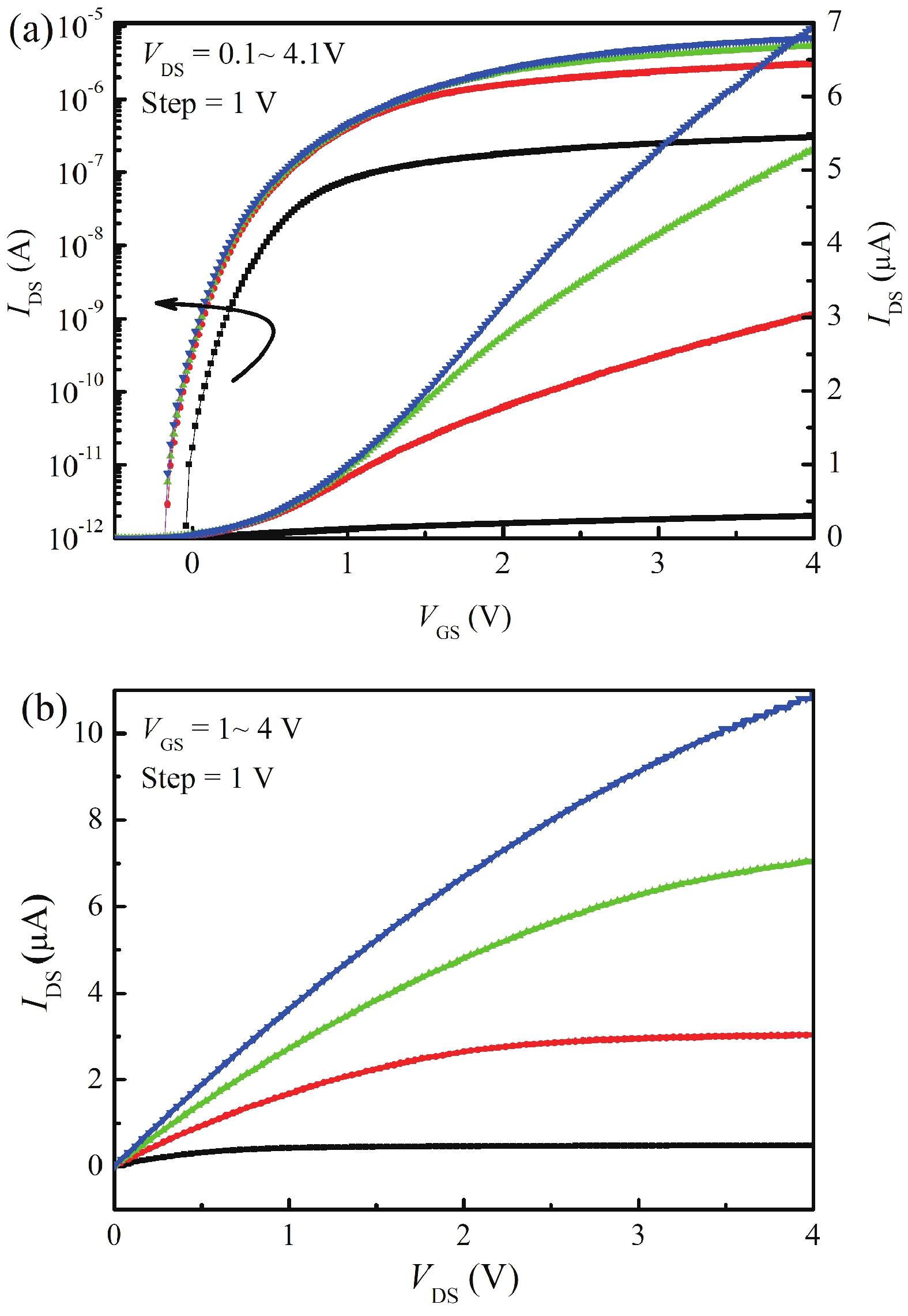
Fig. 3.  (Color online) Measured drain current characteristics at room temperature, showing (a) drain current versus gate voltage for drain voltages of 0.1 to 4.1 V with step of 1 V, and (b) drain current versus drain voltage for gate voltages from 1 to 4 V with step of 1 V.

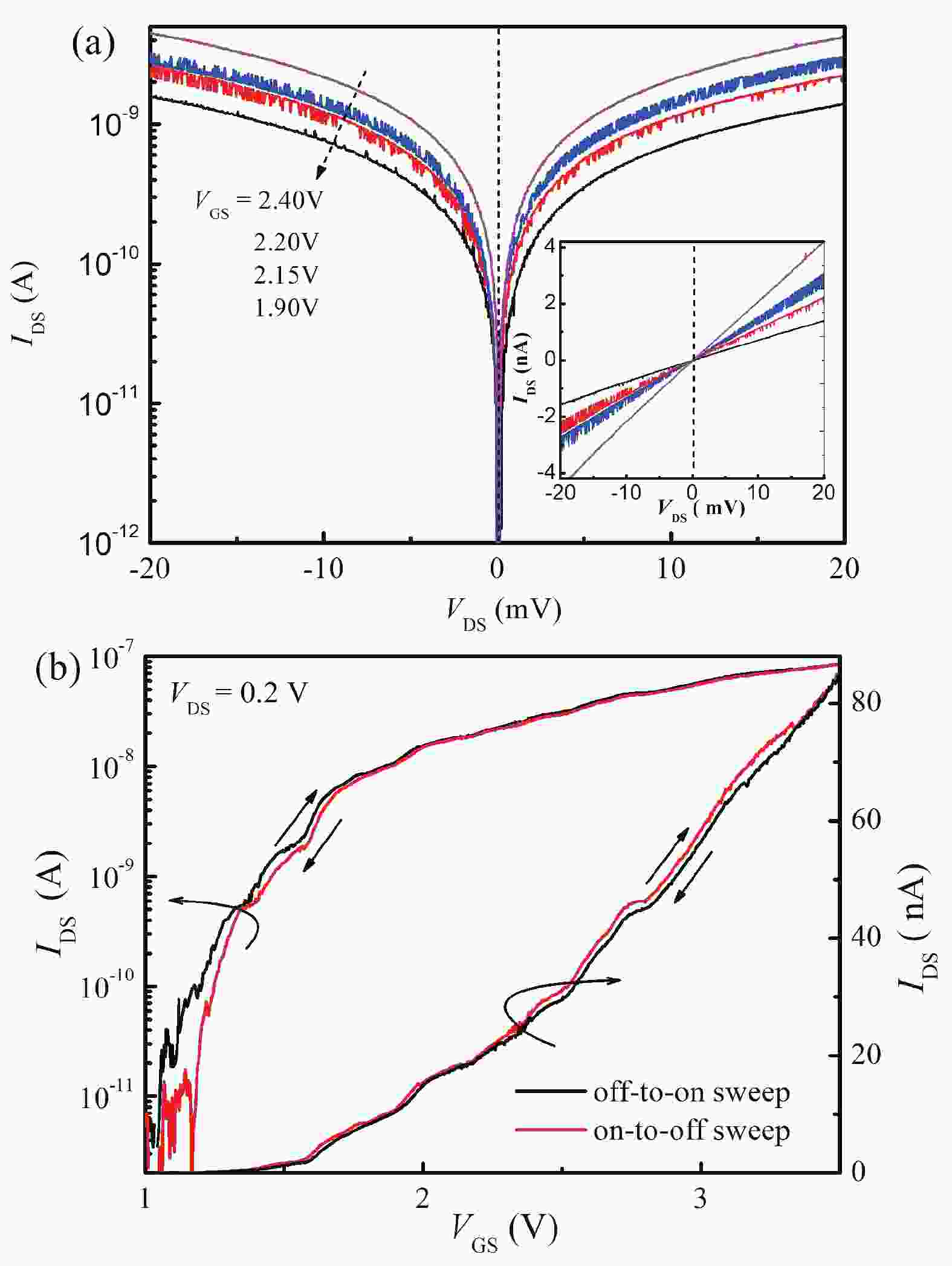
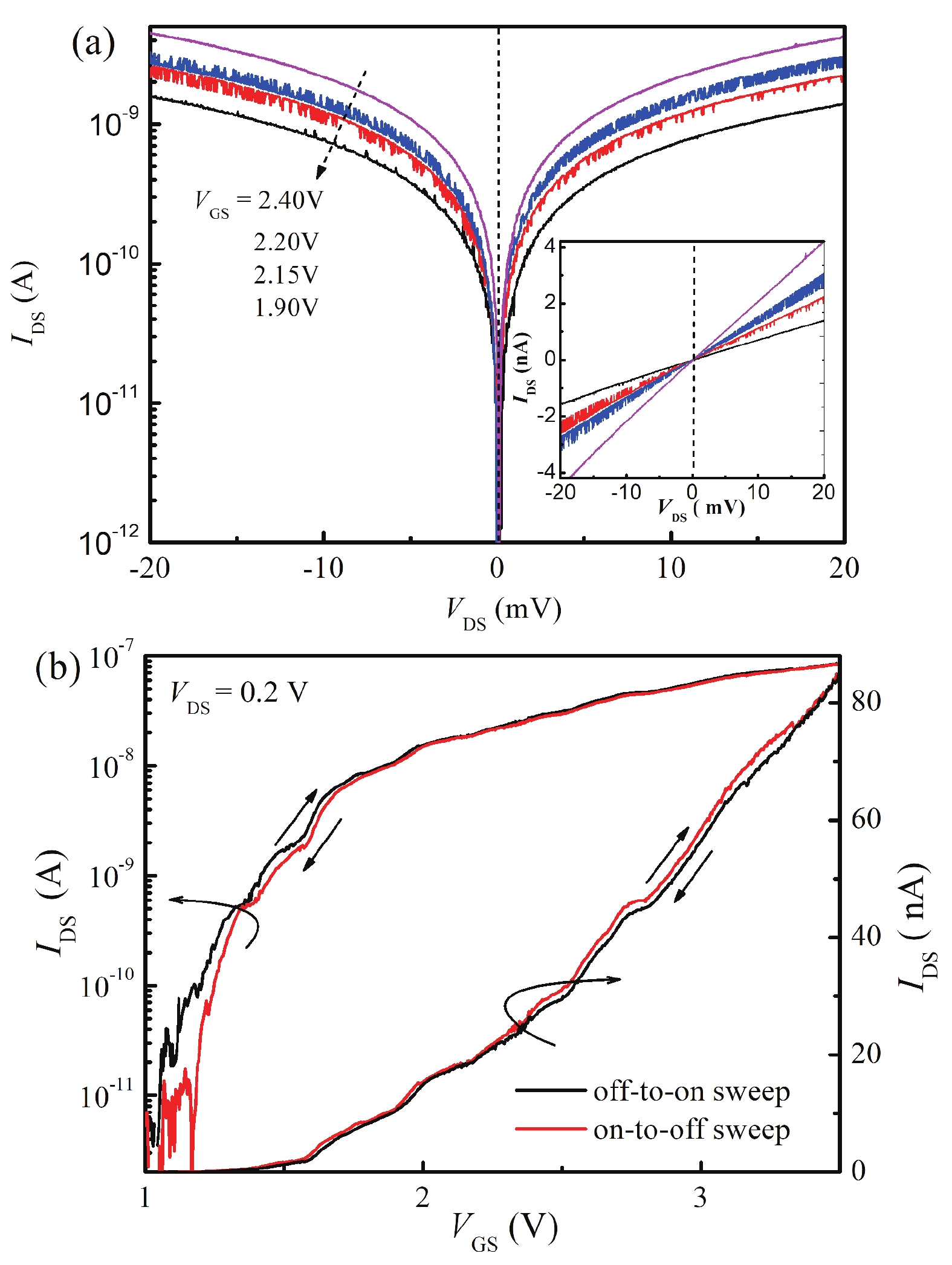
Fig. 4.  (Color online) (a) IDSVDS output characteristics of JNT device at T = 10 K. (b) The transfer characteristics of the JNT with VGS sweep from 0 to 3.5 V and back.

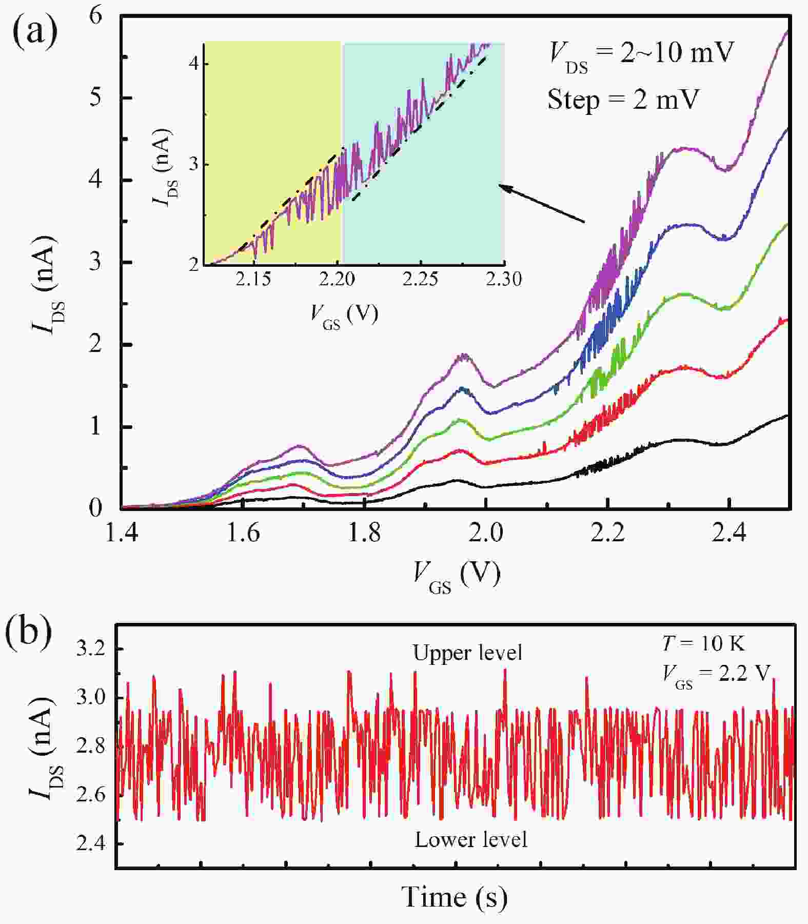
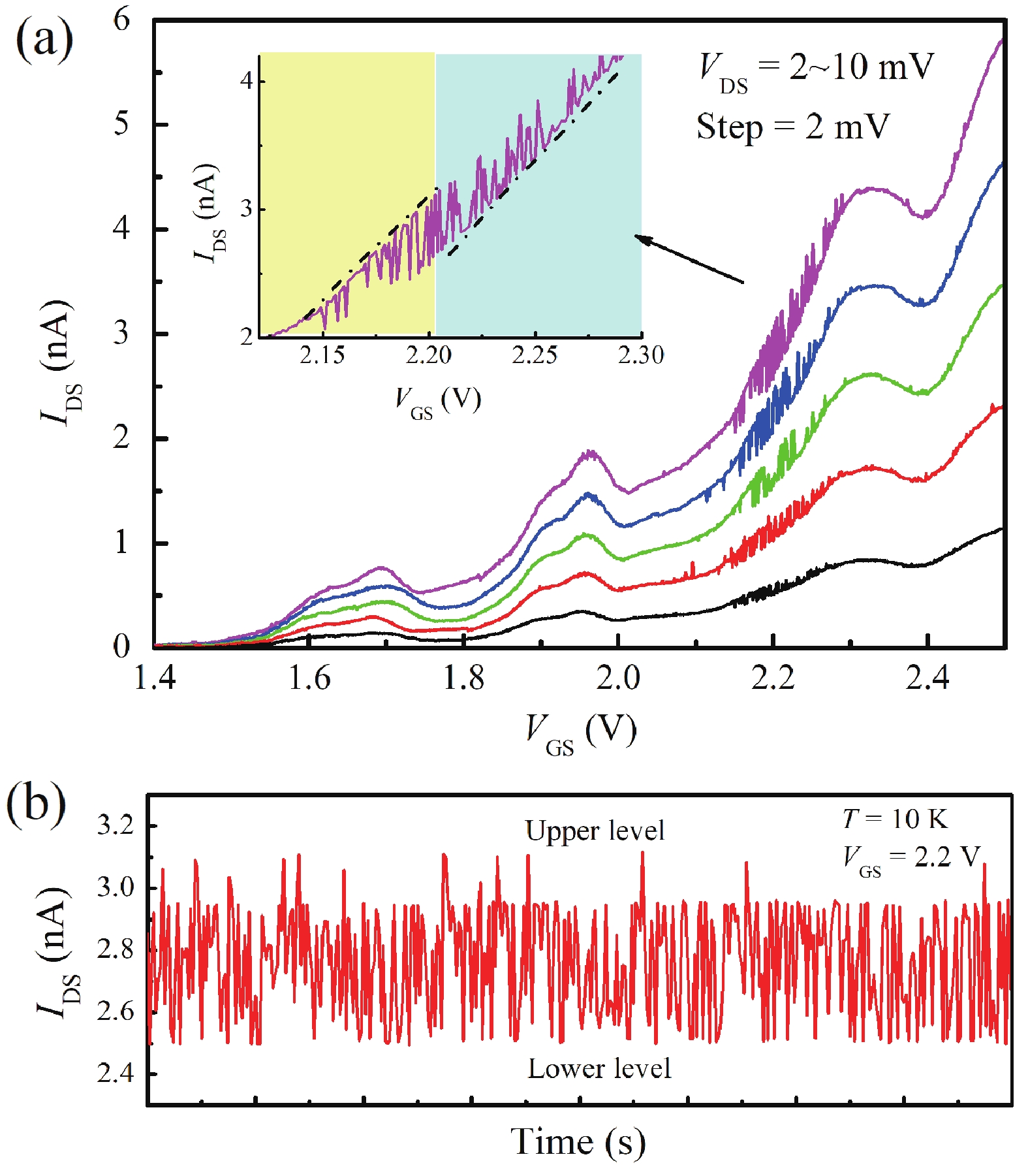
Fig. 5.  (Color online) (a) IDSVGS curves for VDS values ranging from 2 to 10 mV in steps of 2 mV. The detail image in the upper left corner is an enlarged detail. (b) Time domain current levels versus time trace at VGS = 2.2 V and VDS = 10 mV.

Fig. 6.  (Color online) ln(τc/τe) and its linear fitting. The slope is proportional to xT, the position of the traps in the oxide.

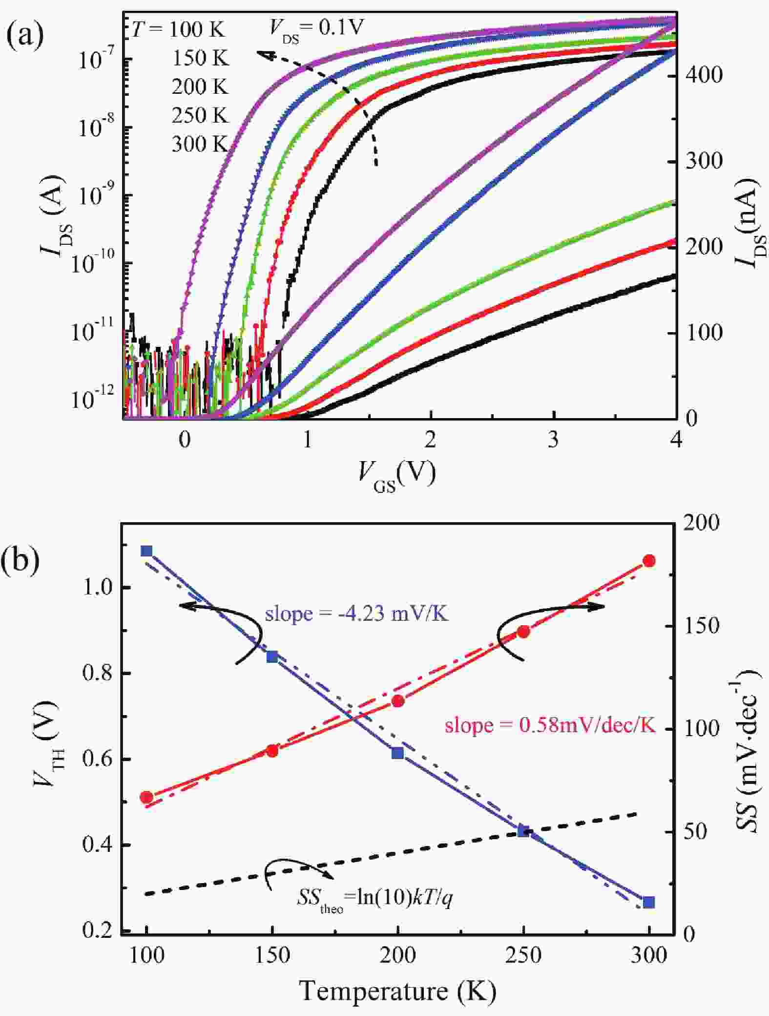
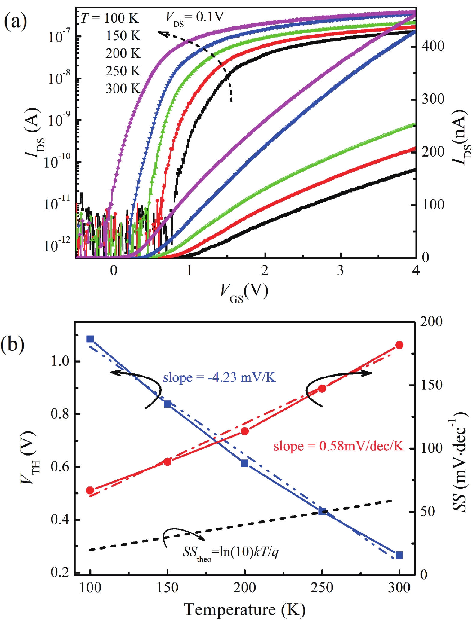
Fig. 7.  (Color online) (a) Transfer characteristics at the temperatures of 100 to 300 K with the step of 50 K. (b) Measured VTH and SS at VDS = 0.1 V versus temperature. The black dashed line represents the theoretical value of subthreshold swing SStheo.

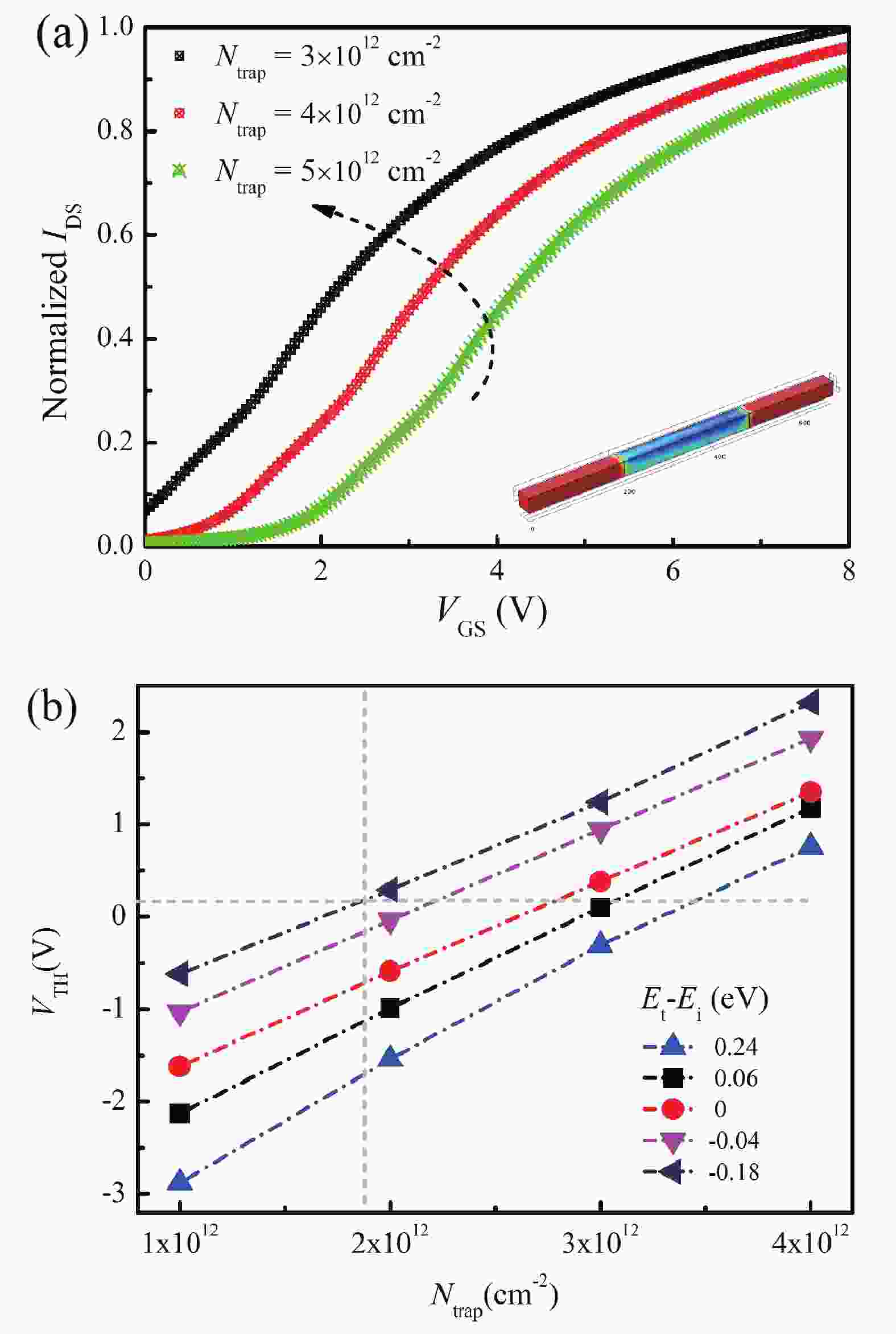
Fig. 8.  (Color online) (a) Simulated IDSVGS curves for different trap densities with the trap level equals to the intrinsic Fermi level. (b) Threshold voltage as a function of trap densities with different trap levels.

[1]
Zhou W H, Zhang S L, Guo S Y, et al. Designing sub-10-nm metal-oxide-semiconductor field-effect transistors via ballistic transport and disparate effective mass: The case of two-dimensional BiN. Phys Rev Appl, 2020, 13(4), 044066 doi: 10.1103/PhysRevApplied.13.044066
[2]
Zhou W H, Zhang S L, Wang Y Y. Anisotropic in-plane ballistic transport in monolayer black arsenic-phosphorus FETs. Adv Electron Mater, 2020, 6(3), 1901281 doi: 10.1002/aelm.201901281
[3]
Jeon D Y, Mouis M, Barraud S, et al. Channel width dependent subthreshold operation of tri-gate junctionless transistors. Solid-State Electron, 2020, 171, 107860 doi: 10.1016/j.sse.2020.107860
[4]
Colinge J P, Lee C W, Afzalian A, et al. Nanowire transistors without junctions. Nat Nanotechnol, 2010, 5, 225 doi: 10.1038/nnano.2010.15
[5]
Mendiratta N, Tripathi S L. A review on performance comparison of advanced MOSFET structures below 45 nm technology node. J Semicond, 2020, 41(6), 061401 doi: 10.1088/1674-4926/41/6/061401
[6]
Lee J, Kim Y, Cho S. Design of poly-Si junctionless Fin-channel FET with quantum-mechanical drift-diffusion models for sub-10-nm technology nodes. IEEE Trans Electron Dev, 2016, 63, 4610 doi: 10.1109/TED.2016.2614990
[7]
Yan R, Kranti A, Ferain I, et al. Investigation of high-performance sub-50 nm junctionless nanowire transistors. Microelectron Reliab, 2011, 51(7), 1166 doi: 10.1016/j.microrel.2011.02.016
[8]
Rudenko T, Nazarov A, Ferain I, et al. Mobility enhancement effect in heavily doped junctionless nanowire silicon-on-insulator metal-oxide-semiconductor field-effect transistors. Appl Phys Lett, 2012, 101, 053511 doi: 10.1063/1.4767353
[9]
Gupta S, Nigam K, Pandey S, et al. Effect of interface trap charges on performance variation of heterogeneous gate dielectric junctionless-TFET. IEEE Trans Electron Dev, 2017, 64(11), 1 doi: 10.1109/TED.2017.2754297
[10]
Nazarov A N, Ferain I, Akhavan N D, et al. Random telegraph-signal noise in junctionless transistors. Appl Phys Lett, 2011, 98(9), 092111 doi: 10.1063/1.3557505
[11]
Berengue O M, Chiquito J. Direct evidence of traps controlling the carriers transport in SnO2 nanobelts. J Semicond, 2017, 38(12), 122001 doi: 10.1088/1674-4926/38/12/122001
[12]
Ma L H, Han W H, Wang H, et al. Charge trapping in surface accumulation layer of heavily doped junctionless nanowire transistors. Chin Phys B, 2015, 024(012), 589 doi: 10.1088/1674-1056/24/12/128101
[13]
Hu G X, Hu S Y, Feng J H, et al. Analytical models for channel potential, threshold voltage, and subthreshold swing of junctionless triple-gate FinFETs. Microelectron J, 2016, 50, 60 doi: 10.1016/j.mejo.2016.02.003
[14]
Liu F Y, Liu H Z, Liu B W, et al. An analytical model for nanowire junctionless SOI FinFETs with considering three-dimensional coupling effect. Chin Phys B, 2016, 25(4), 047305 doi: 10.1088/1674-1056/25/4/047305
[15]
Ávila-Herreraa F, Pazb B C, Cerdeira A. Charge-based compact analytical model for triple-gate junctionless nanowire transistors. Solid-State Electron, 2016, 122(1), 23 doi: 10.1016/j.sse.2016.04.013
[16]
Liang Y Y, Jang Kyungsoo, Velumani S, et al. Effects of interface trap density on the electrical performance of amorphous InSnZnO thin-film transistor. J Semicond, 2015, 36(2), 024007 doi: 10.1088/1674-4926/36/2/024007
[17]
Liu F, Wang K L, Li C, et al. Study of random telegraph signals in single-walled carbon nanotube field effect transistors. IEEE Trans Nanotechnol, 2006, 5(5), 441 doi: 10.1109/TNANO.2006.880906
[18]
Sun Y, Zhang L N, Ahmed Z, et al. Characterization of interface trap dynamics responsible for hysteresis in organic thin-film transistors. Org Electron, 2015, 27, 192 doi: 10.1016/j.orgel.2015.09.011
[19]
Amarasinghe N V, Elik-Butler Z, Vasina P, et al. Characterization of oxide traps in 0.15 μm2 MOSFETs using random telegraph signals. Microelectron Reliab, 2000, 40(11), 1875 doi: 10.1016/S0026-2714(00)00089-5
[20]
Celik-Butler Z, Vasina P. A method for locating the position of oxide traps responsible for random telegraph signals in submicron MOSFETs. IEEE Trans Electron Dev, 2000, 47(3), 646 doi: 10.1109/16.824742
[21]
Cheng Y C, Chen H B, Han M H, et al. Temperature dependence of electronic behaviors in quantum dimension junctionless thin-film transistor. Nanoscale Res Lett, 2014, 9(1), 1 doi: 10.1186/1556-276X-9-392
  • Search

    Advanced Search >>

    GET CITATION

    shu

    Export: BibTex EndNote

    Article Metrics

    Article views: 905 Times PDF downloads: 104 Times Cited by: 0 Times

    History

    Received: 24 December 2021 Revised: 21 January 2022 Online: Accepted Manuscript: 08 April 2022Uncorrected proof: 11 April 2022Published: 01 May 2022

    Catalog

      Email This Article

      User name:
      Email:*请输入正确邮箱
      Code:*验证码错误
      Yifan Fu, Liuhong Ma, Zhiyong Duan, Weihua Han. Effect of charge trapping on electrical characteristics of silicon junctionless nanowire transistor[J]. Journal of Semiconductors, 2022, 43(5): 054101. doi: 10.1088/1674-4926/43/5/054101 Y F Fu, L H Ma, Z Y Duan, W H Han. Effect of charge trapping on electrical characteristics of silicon junctionless nanowire transistor[J]. J. Semicond, 2022, 43(5): 054101. doi: 10.1088/1674-4926/43/5/054101Export: BibTex EndNote
      Citation:
      Yifan Fu, Liuhong Ma, Zhiyong Duan, Weihua Han. Effect of charge trapping on electrical characteristics of silicon junctionless nanowire transistor[J]. Journal of Semiconductors, 2022, 43(5): 054101. doi: 10.1088/1674-4926/43/5/054101

      Y F Fu, L H Ma, Z Y Duan, W H Han. Effect of charge trapping on electrical characteristics of silicon junctionless nanowire transistor[J]. J. Semicond, 2022, 43(5): 054101. doi: 10.1088/1674-4926/43/5/054101
      Export: BibTex EndNote

      Effect of charge trapping on electrical characteristics of silicon junctionless nanowire transistor

      doi: 10.1088/1674-4926/43/5/054101
      More Information
      • Author Bio:

        Yifan Fu was born in 1997. She received a BE degrees in Communication Engineering in 2018 from Northeastern University. She is studying for a master‘s degree at Zhengzhou University

        Liuhong Ma is a lecturer of the School of Physics and Microelectronics, Zhengzhou University. Her reseach interests include nanoelectronic device integration technology and micro-nano processing technology development and nanoscale transistors

        Weihua Han is a research fellow of the Institute of Semiconductors, Chinese Academy of Sciences. His research interests include semiconductor nanostructured electronic and optoelectronic devices and their applications

      • Corresponding author: Email: maliuhong@zzu.edu.cn; Email: weihua@semi.ac.cn
      • Received Date: 2021-12-24
      • Revised Date: 2022-01-21
      • Available Online: 2022-04-08

      Catalog

        /

        DownLoad:  Full-Size Img  PowerPoint
        Return
        Return