


Fig. 1.
(Color online) The simple diagram of the home-made vertical cylindrical dual temperature zone furnace.
ARTICLES
Liyuan Cheng, Hezhi Zhang, Wenhui Zhang and Hongwei Liang
Corresponding author: Hezhi Zhang, hez.zhang@dlut.edu.cn; Hongwei Liang, hwliang@dlut.edu.cn
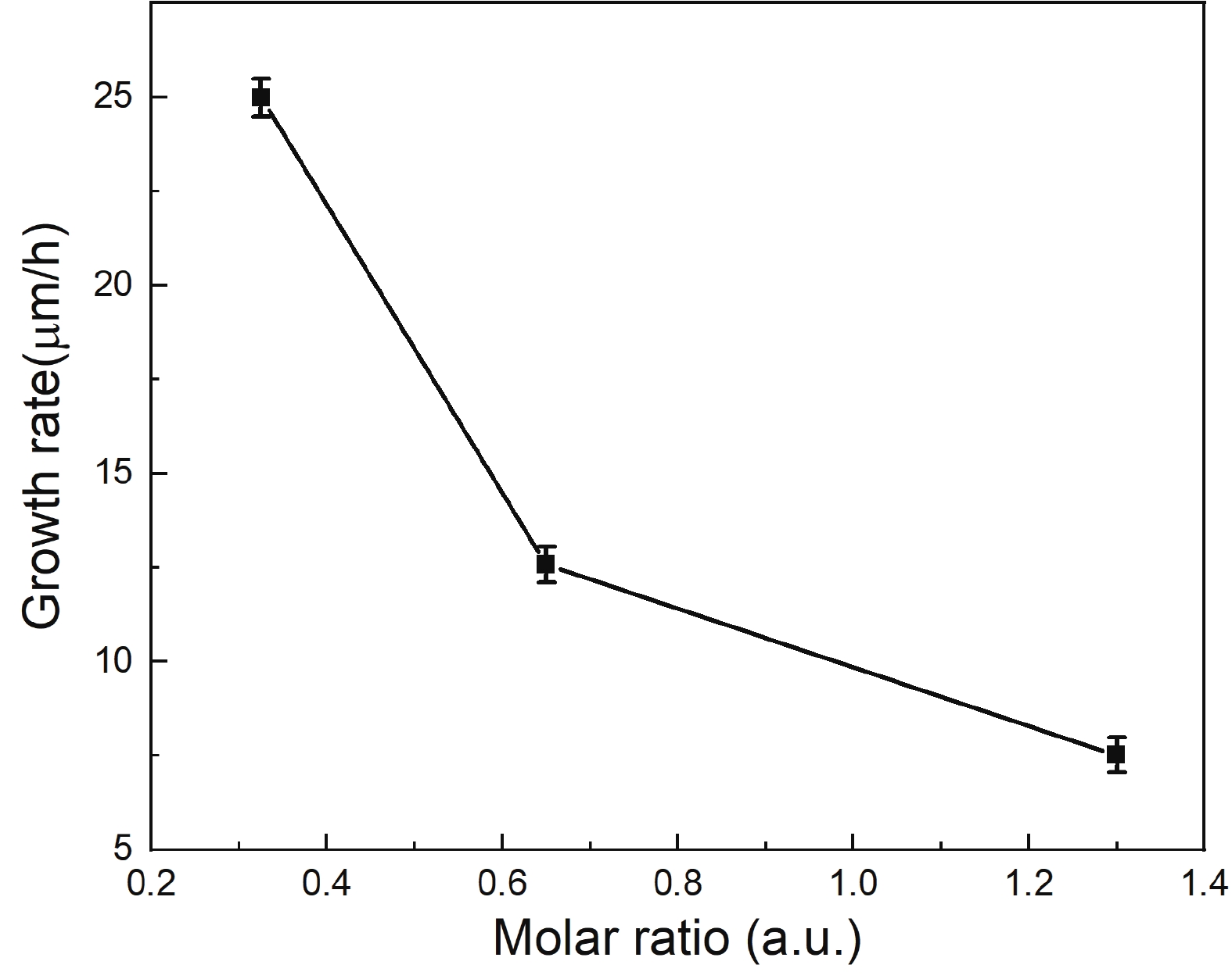
Abstract: We investigated the influence of the growth temperature, O2 flow, molar ratio between Ga2O3 powder and graphite powder on the structure and morphology of the films grown on the c-plane sapphire (0001) substrates by a carbothermal reduction method. Experimental results for the heteroepitaxial growth of β-Ga2O3 illustrate that β-Ga2O3 growth by the carbothermal reduction method can be controlled. The optimal result was obtained at a growth temperature of 1050 °C. The fastest growth rate of β-Ga2O3 films was produced when the O2 flow was 20 sccm. To guarantee that β-Ga2O3 films with both high-quality crystal and morphology properties, the ideal molar ratio between graphite powder and Ga2O3 powder should be set at 10 : 1.
Key words: β-Ga2O3 epitaxy, carbothermal reduction method, growth parameters
| [1] |
Bauman D A, Panov D I, Zakgeim D A, et al. High-quality bulk β-Ga2O3 and β-(AlxGa1–x)2O3 crystals: Growth and properties. Phys Status Solidi A, 2021, 218, 20 doi: 10.1002/pssa.202100335
|
| [2] |
Goyal A, Yadav B S, Thakur O P, et al. Effect of annealing on β-Ga2O3 film grown by pulsed laser deposition technique. J Alloys Compd, 2014, 583, 214 doi: 10.1016/j.jallcom.2013.08.115
|
| [3] |
Sasaki K, Higashiwaki M, Kuramata A, et al. Growth temperature dependences of structural and electrical properties of Ga2O3 epitaxial films grown on β-Ga2O3 (010) substrates by molecular beam epitaxy. Cryst Growth, 2014, 392, 30 doi: 10.1016/j.jcrysgro.2014.02.002
|
| [4] |
Zhang T, Hu Z G, Li Y F, et al. Investigation on the β-Ga2O3 deposited on off-angled sapphire (0001) substrates. J Lumin, 2021, 233, 117928 doi: 10.1016/j.jlumin.2021.117928
|
| [5] |
Kang H C. Heteroepitaxial growth of multidomain Ga2O3/sapphire (001) thin films deposited using radio frequency magnetron sputtering. Mater Lett, 2014, 119, 123 doi: 10.1016/j.matlet.2014.01.030
|
| [6] |
Kamimura T, Sasaki K, Kuramata A, et al. Band alignment and electrical properties of Al2O3 β-Ga2O3 heterojunctions. Appl Phys Lett, 2014, 104, 192104 doi: 10.1063/1.4876920
|
| [7] |
Guo Q X, Hu C Y, Saito K, et al. Growth properties of gallium oxide on sapphire substrate by plasma-assisted pulsed laser depositio. J Semicond, 2019, 40(12), 122801 doi: 10.1088/1674-4926/40/12/122801
|
| [8] |
Oshima T, Okuno T, Fujita S, et al. Ga2O3 thin film growth on c-plane sapphire substrates by molecular beam epitaxy for deep-ultraviolet photodetectors. Jpn J Appl Phys, 2007, 46, 7217 doi: 10.1143/JJAP.46.7217
|
| [9] |
Sasaki K, Kuramata A, Masui T et al. Device-quality β-Ga2O3 epitaxial films fabricated by ozone molecular beam epitaxy. Appl Phys Express, 2012, 5, 035502 doi: 10.1143/APEX.5.035502
|
| [10] |
Higashiwaki M, Sasaki K, Kuramata A, et al. Gallium oxide metal-semiconductor field-effect transistors on single-crystal β-Ga2O3 (010) substrates. Appl Phys Lett, 2012, 100, 013504 doi: 10.1063/1.3674287
|
| [11] |
Zhang Y B, Zheng J, Ma P P, et al. Growth and characterization of β-Ga2O3 thin films grown on off-angled Al2O3 substrates by metal-organic chemical vapor deposition. J Semicond, 2022, 43(9), 092801 doi: 10.1088/1674-4926/43/9/092801
|
| [12] |
Seiler W, Selmane M, Abdelouhadi K, et al. Epitaxial growth of gallium oxide films on c-cut sapphire substrate. Thin Solid Films, 2015, 589, 556 doi: 10.1016/j.tsf.2015.06.034
|
| [13] |
Tak B R, Kumar S, Kapoor A K, et al. Recent advances in the growth of gallium oxide thin films employing various growth techniques-a review. J Phys D, 2021, 54, 453002 doi: 10.1088/1361-6463/ac1af2
|
| [14] |
Hoffmann G, Budde M, Mazzolini P, et al. Efficient suboxide sources in oxide molecular beam epitaxy using mixed metal + oxide charges: The examples of SnO and Ga2O. APL Mater, 2020, 8, 031110 doi: 10.1063/1.5134444
|
| [15] |
Sheoran H, Fang S, Liang F Z, et al. High performance of zero-power-consumption MOCVD-grown β-Ga2O3-based solar-blind photodetectors with ultralow dark current and high-temperature functionalities. Appl Mater Inter, 2022, 14, 52096 doi: 10.1021/acsami.2c08511
|
| [16] |
Qin Y, Li L H, Zhao X L, et al. Metal−semiconductor−metal ε-Ga2O3 solar-blind photodetectors with a record-high responsivity rejection ratio and their gain mechanism. ACS Photonics, 2020, 7, 812 doi: 10.1021/acsphotonics.9b01727
|
| [17] |
Sun H D, Li K H, Castanedo Torres C G, et al. HCl flow-induced phase change of α-, β-, and ε-Ga2O3 films grown by MOCVD. Cryst Growth Des, 2018, 18, 2370 doi: 10.1021/acs.cgd.7b01791
|
| [18] |
Zhuo Y, Chen Z M, Tu W B, et al. β-Ga2O3 versus ε-Ga2O3: Control of the crystal phase composition of gallium oxide thin film prepared by metal-organic chemical vapor deposition. Appl Surf Sci, 2017, 420, 802 doi: 10.1016/j.apsusc.2017.05.241
|
| [19] |
Yao Y, Okur S, Lyle L A M, et al. Growth and characterization of α-, β-, and ε-phases of Ga2O3 using MOCVD and HVPE techniques. Mater Res Lett, 2018, 6, 268 doi: 10.1080/21663831.2018.1443978
|
| [20] |
Bosi M, Mazzolini P, Seravalli L, et al. Ga2O3 polymorphs: tailoring the epitaxial growth conditions. J Mater Chem C, 2020, 8, 10975 doi: 10.1039/D0TC02743J
|
| [21] |
Lee S D, Kaneko K, Fujita S. Homoepitaxial growth of beta gallium oxide films by mist chemical vapor deposition. Jpn J Appl Phys, 2016, 55, 1202B8 doi: 10.7567/JJAP.55.1202B8
|
| [22] |
Nomura K, Goto K, Togashi R, et al. Thermodynamic study of β-Ga2O3 growth by halide vapor phase epitaxy. J Cryst Growth, 2014, 405, 19 doi: 10.1016/j.jcrysgro.2014.06.051
|
| [23] |
Lee J, Kim H, Gautam L, et al. High thermal stability of β-Ga2O3 grown by MOCVD. Crystals, 2021, 11, 446 doi: 10.3390/cryst11040446
|
| [24] |
Zhang W H, Zhang H Z, Liang H W, et al. Heteroepitaxial β-Ga2O3 thick films on sapphire substrate by carbothermal reduction rapid growth method. Semicond Sci Technol, 2022, 37, 085014 doi: 10.1088/1361-6641/ac79c7
|
| [25] |
Qi Q, Chen H F, Hong Z F, et al. Preparation and characteristics of ultra-wide Ga2O3 nanoribbons up to millimeter-long level without catalyst. Acta Physica Sinica, 2020, 69(16), 168101 doi: 10.7498/aps.69.20200481
|
| [26] |
Fukushima J, Takizawa H. Size control of Ti4O7 nanoparticles by carbothermal reduction using a multimode microwave furnace. Crystals, 2018, 8, 444 doi: 10.3390/cryst8120444
|
| [27] |
Maeng S H, Lee H, Park M S, et al. Ultrafast carbothermal reduction of silica to silicon using a CO2 laser beam. Sci Rep, 2020, 10, 21730 doi: 10.1038/s41598-020-78562-1
|
| [28] |
Mazzolini P, Falkenstein A, Wouters C, et al. Offcut-related step-flow and growth rate enhancement during (100) β-Ga2O3 homoepitaxy by metal-exchange catalyzed molecular beam epitaxy. APL Mater, 2020, 8, 011107 doi: 10.1063/1.5135772
|
| [29] |
Vogt P, Bierwagen O. Reaction kinetics and growth window for plasma-assisted molecular beam epitaxy of Ga2O3: Incorporation of Ga vs. Ga2O desorption. Appl Phys Lett, 2016, 108, 072101 doi: 10.1063/1.4942002
|
| [30] |
Vogt P, Bierwagen O. Comparison of the growth kinetics of In2O3 and Ga2O3 and their suboxide desorption during plasma-assisted molecular beam epitaxy. Appl Phys Lett, 2016, 109, 062103 doi: 10.1063/1.4960633
|
| [31] |
Hu D Q, Zhuang S W, Ma Z Z, et al. Study on the optical properties of β-Ga2O3 films grown by MOCVD. J Mater Sci, 2017, 28, 10997 doi: 10.1007/s10854-017-6882-x
|
| [32] |
An Y X, Dai L Y, Wu Y, et al. Epitaxial growth of β-Ga2O3 thin films on Ga2O3 and Al2O3 substrates by using pulsed laser deposition. JAD, 2019, 9, 1950032 doi: 10.1142/S2010135X19500322
|
| [33] |
Blumenschein N, Paskova T, Muth J F. Effect of growth pressure on PLD-deposited gallium oxide thin films for deep-UV photodetectors. Phys Status Solidi A, 2019, 216, 1900098 doi: 10.1002/pssa.201900098
|
| [34] |
Alhalaili B, Mao H, Dryden D M, et al. Influence of silver as a catalyst on the growth of β-Ga2O3 nanowires on GaAs. Materials, 2020, 13, 5377 doi: 10.3390/ma13235377
|
| [35] |
Feng B Y, Li Z C, Cheng F Y, et al. Investigation of β-Ga2O3 film growth mechanism on c-plane sapphire substrate by ozone molecular beam epitaxy. Phys Status Solidi A, 2021, 218, 2000457 doi: 10.1002/pssa.202000457
|
| [36] |
Sun H D, Castanedo Torres C G, Liu K K, et al. Valence and conduction band offsets of β-Ga2O3/AlN heterojunction. Appl Phys Lett, 2017, 111, 162105 doi: 10.1063/1.5003930
|
| [37] |
Nakagomi S, Kokubun Y. Crystal orientation of β-Ga2O3 thin films formed on c-plane and a-plane sapphire substrate. J Cryst Growth, 2012, 349, 12 doi: 10.1016/j.jcrysgro.2012.04.006
|
| [38] |
Guo D Y, Wu Z P, Li P G, et al. Fabrication of β-Ga2O3 thin films and solar-blind photodetectors by laser MBE technology. Opt Mater Express, 2014, 4, 1067 doi: 10.1364/OME.4.001067
|


Article views: 1685 Times PDF downloads: 113 Times Cited by: 0 Times
Received: 31 December 2022 Revised: 13 March 2023 Online: Accepted Manuscript: 20 March 2023Uncorrected proof: 21 March 2023Corrected proof: 22 May 2023Published: 08 June 2023
| Citation: |
Liyuan Cheng, Hezhi Zhang, Wenhui Zhang, Hongwei Liang. Investigation of β-Ga2O3 thick films grown on c-plane sapphire via carbothermal reduction[J]. Journal of Semiconductors, 2023, 44(6): 062804. doi: 10.1088/1674-4926/44/6/062804
****
L Y Cheng, H Z Zhang, W H Zhang, H W Liang. Investigation of β-Ga2O3 thick films grown on c-plane sapphire via carbothermal reduction[J]. J. Semicond, 2023, 44(6): 062804. doi: 10.1088/1674-4926/44/6/062804

|
 Liyuan Cheng:received her Bachelor’s degree from University of Jinan in 2020. She is currently pursuing a Master’s degree at the School of Microelectronics, Dalian University of Technology at Dalian, China, under the supervision of Prof. Hezhi Zhang. Her research interests center on the growth of β-Ga2O3
 Hezhi Zhang:received his Master’s degree from Dalian University of Technology, Dalian, China in 2012 and Ph.D. degree from the Paris-Saclay University, Paris, France in 2016. He joined École Polytechnique Fédérale de Lausanne as a postdoc researcher in August 2016. In 2019, he joined the Dalian University of Technology as an associate professor. His research interests focus on the wide bandgap semiconductor materials and power devices
 Wenhui Zhang:received her Master’s degree from Liaoning Normal University, Liaoning, China. She is currently working toward the Ph.D. degree at the Dalian university of Technology, Liaoning, China. Her research interests center on ultra-wide bandgap semiconductor of β-Ga2O3
 Hongwei Liang:is a professor in the School of Microelectronics, Dalian University of Technology, Dalian, China. He received his Ph.D. degree from Changchun Institute of Optical Machinery and Physics, Chinese Academy of Sciences, Changchun, China. In 2005, he joined the Dalian University of Technology. His research interests include wide bandgap semiconductor detector, HEMT devices and biosensors, the third generation of semiconductor light-emitting devices
| [1] |
Bauman D A, Panov D I, Zakgeim D A, et al. High-quality bulk β-Ga2O3 and β-(AlxGa1–x)2O3 crystals: Growth and properties. Phys Status Solidi A, 2021, 218, 20 doi: 10.1002/pssa.202100335
|
| [2] |
Goyal A, Yadav B S, Thakur O P, et al. Effect of annealing on β-Ga2O3 film grown by pulsed laser deposition technique. J Alloys Compd, 2014, 583, 214 doi: 10.1016/j.jallcom.2013.08.115
|
| [3] |
Sasaki K, Higashiwaki M, Kuramata A, et al. Growth temperature dependences of structural and electrical properties of Ga2O3 epitaxial films grown on β-Ga2O3 (010) substrates by molecular beam epitaxy. Cryst Growth, 2014, 392, 30 doi: 10.1016/j.jcrysgro.2014.02.002
|
| [4] |
Zhang T, Hu Z G, Li Y F, et al. Investigation on the β-Ga2O3 deposited on off-angled sapphire (0001) substrates. J Lumin, 2021, 233, 117928 doi: 10.1016/j.jlumin.2021.117928
|
| [5] |
Kang H C. Heteroepitaxial growth of multidomain Ga2O3/sapphire (001) thin films deposited using radio frequency magnetron sputtering. Mater Lett, 2014, 119, 123 doi: 10.1016/j.matlet.2014.01.030
|
| [6] |
Kamimura T, Sasaki K, Kuramata A, et al. Band alignment and electrical properties of Al2O3 β-Ga2O3 heterojunctions. Appl Phys Lett, 2014, 104, 192104 doi: 10.1063/1.4876920
|
| [7] |
Guo Q X, Hu C Y, Saito K, et al. Growth properties of gallium oxide on sapphire substrate by plasma-assisted pulsed laser depositio. J Semicond, 2019, 40(12), 122801 doi: 10.1088/1674-4926/40/12/122801
|
| [8] |
Oshima T, Okuno T, Fujita S, et al. Ga2O3 thin film growth on c-plane sapphire substrates by molecular beam epitaxy for deep-ultraviolet photodetectors. Jpn J Appl Phys, 2007, 46, 7217 doi: 10.1143/JJAP.46.7217
|
| [9] |
Sasaki K, Kuramata A, Masui T et al. Device-quality β-Ga2O3 epitaxial films fabricated by ozone molecular beam epitaxy. Appl Phys Express, 2012, 5, 035502 doi: 10.1143/APEX.5.035502
|
| [10] |
Higashiwaki M, Sasaki K, Kuramata A, et al. Gallium oxide metal-semiconductor field-effect transistors on single-crystal β-Ga2O3 (010) substrates. Appl Phys Lett, 2012, 100, 013504 doi: 10.1063/1.3674287
|
| [11] |
Zhang Y B, Zheng J, Ma P P, et al. Growth and characterization of β-Ga2O3 thin films grown on off-angled Al2O3 substrates by metal-organic chemical vapor deposition. J Semicond, 2022, 43(9), 092801 doi: 10.1088/1674-4926/43/9/092801
|
| [12] |
Seiler W, Selmane M, Abdelouhadi K, et al. Epitaxial growth of gallium oxide films on c-cut sapphire substrate. Thin Solid Films, 2015, 589, 556 doi: 10.1016/j.tsf.2015.06.034
|
| [13] |
Tak B R, Kumar S, Kapoor A K, et al. Recent advances in the growth of gallium oxide thin films employing various growth techniques-a review. J Phys D, 2021, 54, 453002 doi: 10.1088/1361-6463/ac1af2
|
| [14] |
Hoffmann G, Budde M, Mazzolini P, et al. Efficient suboxide sources in oxide molecular beam epitaxy using mixed metal + oxide charges: The examples of SnO and Ga2O. APL Mater, 2020, 8, 031110 doi: 10.1063/1.5134444
|
| [15] |
Sheoran H, Fang S, Liang F Z, et al. High performance of zero-power-consumption MOCVD-grown β-Ga2O3-based solar-blind photodetectors with ultralow dark current and high-temperature functionalities. Appl Mater Inter, 2022, 14, 52096 doi: 10.1021/acsami.2c08511
|
| [16] |
Qin Y, Li L H, Zhao X L, et al. Metal−semiconductor−metal ε-Ga2O3 solar-blind photodetectors with a record-high responsivity rejection ratio and their gain mechanism. ACS Photonics, 2020, 7, 812 doi: 10.1021/acsphotonics.9b01727
|
| [17] |
Sun H D, Li K H, Castanedo Torres C G, et al. HCl flow-induced phase change of α-, β-, and ε-Ga2O3 films grown by MOCVD. Cryst Growth Des, 2018, 18, 2370 doi: 10.1021/acs.cgd.7b01791
|
| [18] |
Zhuo Y, Chen Z M, Tu W B, et al. β-Ga2O3 versus ε-Ga2O3: Control of the crystal phase composition of gallium oxide thin film prepared by metal-organic chemical vapor deposition. Appl Surf Sci, 2017, 420, 802 doi: 10.1016/j.apsusc.2017.05.241
|
| [19] |
Yao Y, Okur S, Lyle L A M, et al. Growth and characterization of α-, β-, and ε-phases of Ga2O3 using MOCVD and HVPE techniques. Mater Res Lett, 2018, 6, 268 doi: 10.1080/21663831.2018.1443978
|
| [20] |
Bosi M, Mazzolini P, Seravalli L, et al. Ga2O3 polymorphs: tailoring the epitaxial growth conditions. J Mater Chem C, 2020, 8, 10975 doi: 10.1039/D0TC02743J
|
| [21] |
Lee S D, Kaneko K, Fujita S. Homoepitaxial growth of beta gallium oxide films by mist chemical vapor deposition. Jpn J Appl Phys, 2016, 55, 1202B8 doi: 10.7567/JJAP.55.1202B8
|
| [22] |
Nomura K, Goto K, Togashi R, et al. Thermodynamic study of β-Ga2O3 growth by halide vapor phase epitaxy. J Cryst Growth, 2014, 405, 19 doi: 10.1016/j.jcrysgro.2014.06.051
|
| [23] |
Lee J, Kim H, Gautam L, et al. High thermal stability of β-Ga2O3 grown by MOCVD. Crystals, 2021, 11, 446 doi: 10.3390/cryst11040446
|
| [24] |
Zhang W H, Zhang H Z, Liang H W, et al. Heteroepitaxial β-Ga2O3 thick films on sapphire substrate by carbothermal reduction rapid growth method. Semicond Sci Technol, 2022, 37, 085014 doi: 10.1088/1361-6641/ac79c7
|
| [25] |
Qi Q, Chen H F, Hong Z F, et al. Preparation and characteristics of ultra-wide Ga2O3 nanoribbons up to millimeter-long level without catalyst. Acta Physica Sinica, 2020, 69(16), 168101 doi: 10.7498/aps.69.20200481
|
| [26] |
Fukushima J, Takizawa H. Size control of Ti4O7 nanoparticles by carbothermal reduction using a multimode microwave furnace. Crystals, 2018, 8, 444 doi: 10.3390/cryst8120444
|
| [27] |
Maeng S H, Lee H, Park M S, et al. Ultrafast carbothermal reduction of silica to silicon using a CO2 laser beam. Sci Rep, 2020, 10, 21730 doi: 10.1038/s41598-020-78562-1
|
| [28] |
Mazzolini P, Falkenstein A, Wouters C, et al. Offcut-related step-flow and growth rate enhancement during (100) β-Ga2O3 homoepitaxy by metal-exchange catalyzed molecular beam epitaxy. APL Mater, 2020, 8, 011107 doi: 10.1063/1.5135772
|
| [29] |
Vogt P, Bierwagen O. Reaction kinetics and growth window for plasma-assisted molecular beam epitaxy of Ga2O3: Incorporation of Ga vs. Ga2O desorption. Appl Phys Lett, 2016, 108, 072101 doi: 10.1063/1.4942002
|
| [30] |
Vogt P, Bierwagen O. Comparison of the growth kinetics of In2O3 and Ga2O3 and their suboxide desorption during plasma-assisted molecular beam epitaxy. Appl Phys Lett, 2016, 109, 062103 doi: 10.1063/1.4960633
|
| [31] |
Hu D Q, Zhuang S W, Ma Z Z, et al. Study on the optical properties of β-Ga2O3 films grown by MOCVD. J Mater Sci, 2017, 28, 10997 doi: 10.1007/s10854-017-6882-x
|
| [32] |
An Y X, Dai L Y, Wu Y, et al. Epitaxial growth of β-Ga2O3 thin films on Ga2O3 and Al2O3 substrates by using pulsed laser deposition. JAD, 2019, 9, 1950032 doi: 10.1142/S2010135X19500322
|
| [33] |
Blumenschein N, Paskova T, Muth J F. Effect of growth pressure on PLD-deposited gallium oxide thin films for deep-UV photodetectors. Phys Status Solidi A, 2019, 216, 1900098 doi: 10.1002/pssa.201900098
|
| [34] |
Alhalaili B, Mao H, Dryden D M, et al. Influence of silver as a catalyst on the growth of β-Ga2O3 nanowires on GaAs. Materials, 2020, 13, 5377 doi: 10.3390/ma13235377
|
| [35] |
Feng B Y, Li Z C, Cheng F Y, et al. Investigation of β-Ga2O3 film growth mechanism on c-plane sapphire substrate by ozone molecular beam epitaxy. Phys Status Solidi A, 2021, 218, 2000457 doi: 10.1002/pssa.202000457
|
| [36] |
Sun H D, Castanedo Torres C G, Liu K K, et al. Valence and conduction band offsets of β-Ga2O3/AlN heterojunction. Appl Phys Lett, 2017, 111, 162105 doi: 10.1063/1.5003930
|
| [37] |
Nakagomi S, Kokubun Y. Crystal orientation of β-Ga2O3 thin films formed on c-plane and a-plane sapphire substrate. J Cryst Growth, 2012, 349, 12 doi: 10.1016/j.jcrysgro.2012.04.006
|
| [38] |
Guo D Y, Wu Z P, Li P G, et al. Fabrication of β-Ga2O3 thin films and solar-blind photodetectors by laser MBE technology. Opt Mater Express, 2014, 4, 1067 doi: 10.1364/OME.4.001067
|

 WeChat ID
Journal of Semiconductors © 2017 All Rights Reserved 京ICP备05085259号-2

 DownLoad:

