


1. Introduction
Due to the low background noise and high sensitivity, the solar-blind ultraviolet (UV) photodetectors can be widely used in flame detection, ozone monitoring, missile tracking and space communication[1-5]. Solar-blind photodetectors are usually fabricated from wide bandgap semiconductor materials, including AlGaN[1, 6], MgZnO[7, 8], diamond[9-11], and Ga2O3[12-15]. Among these materials, β-Ga2O3 is the most desirable semiconductor material for solar-blind UV detection due to its suitable bandgap with a unique bandgap structure and relative easiness in preparation. At present, high-performance gallium oxide-based photodetectors have been widely reported[16-21].
β-Ga2O3 is a binary compound semiconductor with a bandgap of about 4.9 eV. The optical absorption edge wavelength of β-Ga2O3 is less than 280 nm, and its absorption coefficient for solar-blind UV light can reach 105 cm−1, which is conducive for achieving high performance photoelectric detection. In addition, the theoretical breakdown field strength of β-Ga2O3 can reach 8 MV/cm[22]. Its Baliga’s figure of merit (BFOM) can reach 3214, which is much higher than that of SiC and GaN materials[23]. It also has good chemical stability and thermal stability. And it can be prepared by various methods. These advantages make it have great application potential for the fabrication of solar-blind UV photodetector and high-power electronic devices.
In the past few years, the research of solar-blind UV photodetectors based on different forms of Ga2O3 has been widely reported, including bulk materials, thin film and micro-nano structure[24-28]. Among them, single crystal materials have high crystalline quality but are relatively expensive. Ga2O3 thin films can be grown through various methods, but the crystal quality still needs to be improved. Compared with the former two, micro-nano structure not only has high crystalline quality but also has relatively low cost. Recently, β-Ga2O3 micro-nano materials have been widely studied because of their rich morphology and excellent performance[29-31].
In this paper, we demonstrate the preparation of β-Ga2O3 microwires (MWs) and the realization of high-performance MSM photodetectors based on β-Ga2O3 MWs. The high crystal quality centimeter-length β-Ga2O3 MWs were synthesized via a chemical vapor deposition method (CVD). The maximum peak responsivity of the device is 1.2 A/W at 240 nm with an ultrahigh UV/visible rejection ratio (Rpeak/R400 nm) of 5.8 × 10⁵, indicating that the device has excellent spectral selectivity. In addition, no obvious persistent photoconductivity was observed in the device. The rise and decay time constants of the device were 0.13 and 0.14 s, respectively. This work not only provides a growth method for high-quality Ga2O3 MWs, but also demonstrates the excellent performance of Ga2O3 MWs in solar-blind ultraviolet detection.
2. Experimental
The β-Ga2O3 MWs were synthesized with traditional chemical vapor deposition (CVD) with a horizontal tube furnace. The source material, which is a mixture of β-Ga2O3 and graphite powders with a definite weight ratio of 1 : 1, was placed at the center of a corundum boat. A clean silicon substrate was fixed on the top of the corundum boat. The growth temperature was kept at 1100 °C for 30 min. During the synthetic process, a constant flow of argon (99.999%) (120 standard cubic centimeters per minute) was introduced into the tube furnace as the carrier gas. After the reaction, the furnace was cooled down to room temperature naturally and the β-Ga2O3 MWs were obtained on the surface of the corundum boat.
The morphologies of the β-Ga2O3 MWs were investigated by a field-emission scanning electron microscopy (FESEM) and a transmission electron microscope (TEM). The crystal structure was studied by X-ray diffraction (XRD). The I–V and I–t characteristics of the devices were measured by a semiconductor characterization system (Keithley 4200 system) with a Xe lamp and a monochromator. The time resolved spectrum was collected by an oscilloscope (Tektronix TBS 1102).
3. Results and discussion
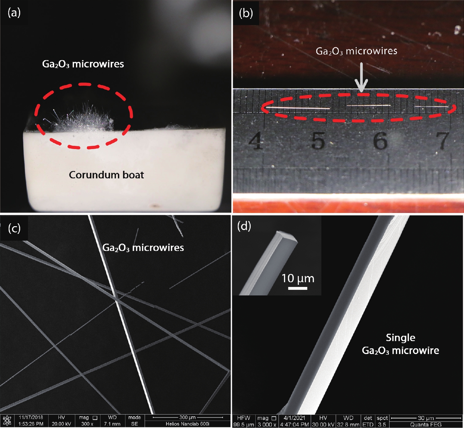
Fig. 1(a) is an image of the Ga2O3 MW just taken out of the tube furnace. It can be seen that there are microwire clusters on the wall of the corundum boat. The growth of microwires follows vapor–solid (V–S) mode without the participation of metal catalysts[31]. Ga2O3 is reduced by carbon powder at high temperature and reacts with oxygen to regenerate Ga2O3, which condenses and grows on the rough corundum boat wall. In the experiment, it was found that Ga2O3 MWs are hardly grown on smooth surfaces. The reason is that the growth of microwires requires nucleation sites and a rough surface is easier to nucleate. Therefore, Ga2O3 MWs tend to grow on the rough corundum boat wall, which is the same as reported in other works[31]. In order to display the length scale information of the Ga2O3 MWs, several MWs were placed on a metric ruler, as shown in Fig. 1(b). It can be seen from the figure that the Ga2O3 MWs are relatively long with the longest reaching the length of 1 cm. Usually, the size of micro-nano materials is small and needs to be operated with the help of special equipment. Large-size microwires are more convenient for the subsequent device preparation. Fig. 1(c) is the SEM image of Ga2O3 MWs. It can be seen that the microwires are uniform in thickness. Fig. 1(d) is a SEM image of a single Ga2O3 MW. It can be seen that the surface of the microwire is smooth and the edges are clear. The inset is the cross-sectional image of the microwire. It is obvious that the cross section of the microwire is a regular quadrilateral with a side length of about 10 μm. The cross-sectional shape may be related to the lattice structure of the Ga2O3.

 DownLoad:
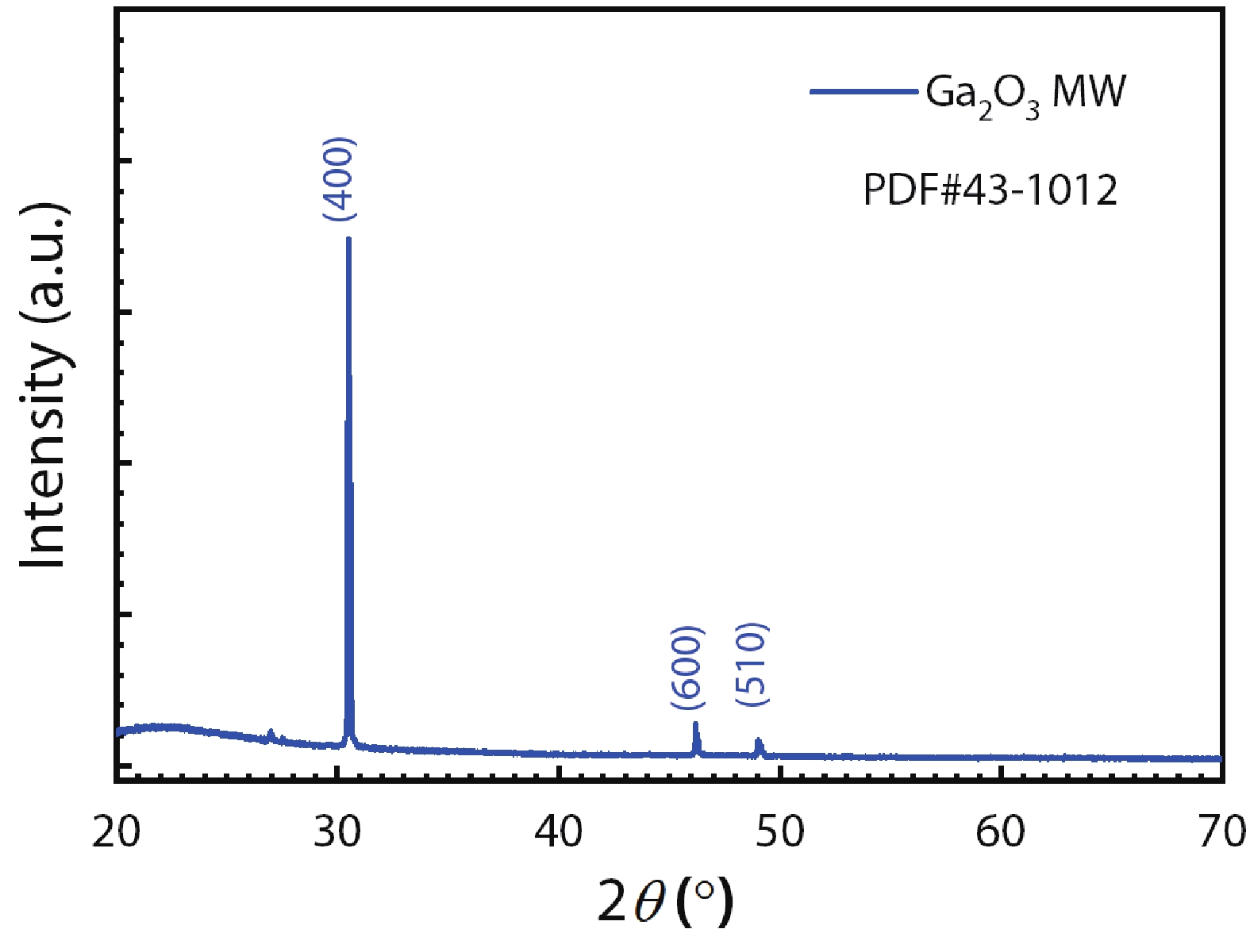
Fig. 2 shows the XRD curve of the Ga2O3 MWs. Before the measurement, Ga2O3 MWs were carefully arranged and fixed on a clean quartz glass substrate. Three XRD peaks can be clearly observed in the figure. By comparing with standard PDF card (No. 43-1012), it can be determined that the diffraction peaks at 30.51°, 46.22°, and 49.12° correspond to the (400), (600), and (510) crystal planes of monoclinic β-Ga2O3, respectively.

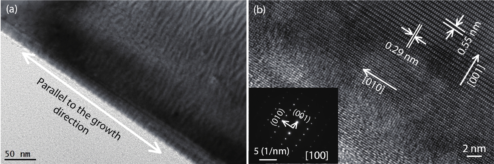
To further explore the crystalline quality of the microwires, a transmission electron microscopy measurement was performed. Fig. 3(a) is an image of the microwires at low magnification. The growth direction of β-Ga2O3 MWs is given in the figure. Fig. 3(b) is a TEM image of the microwire at high magnification. It can be seen from the figure that the β-Ga2O3 MW is a single crystalline with perfect lattice arrangement of atoms. No obvious lattice defects were observed within the test range, indicating that the prepared β-Ga2O3 MWs had very low defect density. The atomic spacing in the vertical direction is marked in the figure. The spacing of 0.55 and 0.29 nm correspond to the spacing between the (001) and (010) planes, respectively, of monoclinic β-Ga2O3. The measured SAED pattern of the microwire is displayed in the inset of Fig. 3(b), in which the diffraction spots of (001) and (010) planes can be easily found. The SAED pattern indicates the high single crystallinity in the test area.

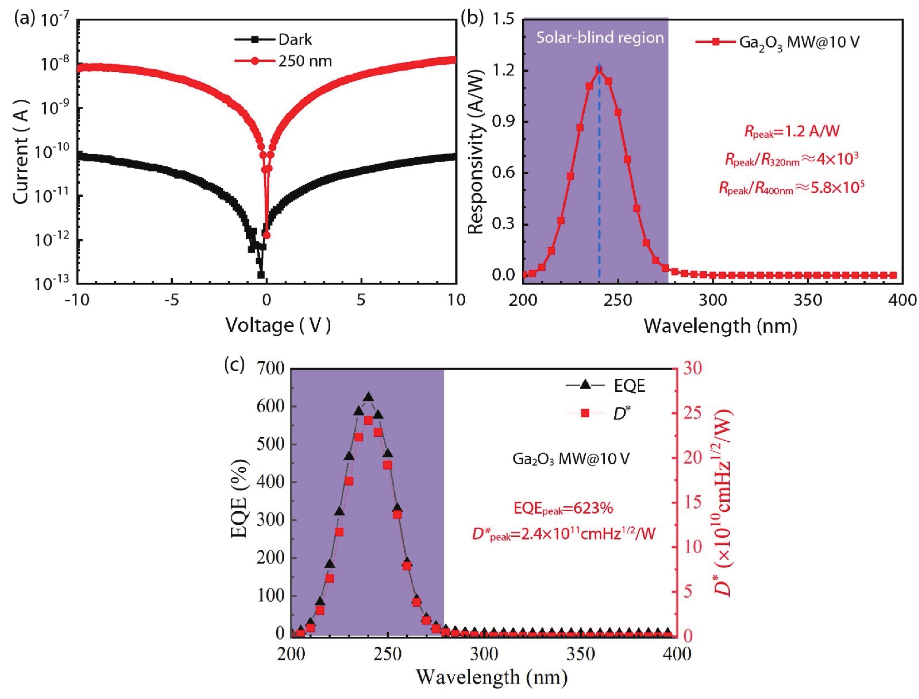
In order to study the photoelectric properties of the microwires, MSM detector structures were fabricated based on β-Ga2O3 MWs. Indium is used as Ohmic contact electrodes with an electrode spacing of 1 mm. Fig. 4(a) shows the I–V curves of the device under dark and 250 nm illumination. It can be found that the dark current of the device can be as low as 78 pA at 10 V bias. Under the illumination of light with a wavelength of 250 nm, the current of the device changed significantly. The ratio of photocurrent and dark current can reach 102, indicating that the device has a good response to solar-blind ultraviolet light. The responsivity of the photodetector can be calculated by the following equation[1]

| Rλ=Iphoto−IdarkPS, |
where Iphoto is the photocurrent, Idark is the dark current, P is the light intensity, and S is the effective illumination area. Fig. 4(b) shows the photoresponsivity of the device in the wavelengths range of 200–400 nm under a bias voltage of 10 V. Obviously, the response wave band of the device is mainly located in the solar-blind ultraviolet region. The peak response appears at around 240 nm with a value of 1.2 A/W. The rejection ratio at peak and 400 nm is about 5.8 × 10⁵, indicating that the device has excellent spectral selectivity.
External quantum efficiency (EQE) and detectivity (D*) are also two important parameters to assess device performance. The EQE reflects the photoelectric conversion efficiency of the device, and the detectivity reflects the detection ability of the device to weak light signals. They can be calculated by the following formulas[14]
| EQE=hcRλqλ, |
| D∗=Rλ√2qJd, |
where h is Planck’s constant, c is the velocity of light, q is the electronic charge, λ is wavelength of the light, and Jd is the optical power density. Fig. 4(c) shows the result of the EQE and D* in the wavelength range of 200–400 nm. From the figure, it can be seen that the peak value of EQE is 623% which is more than 100%. Such a high value is due to the existence of photoconductive gain. The reason for the existence of photoconductive gain may be due to the different mobility of electrons and holes in β-Ga2O3 MWs. When the photogenerated carriers are separated under the external electric field, the electrons are collected by the electrode faster than the holes. In order to maintain the electrical neutrality inside the material, electrons are injected from the electrode into the semiconductor material, resulting in gain and improved external quantum efficiency[32-34]. The peak value of D* was 2.4 × 1011 cm·Hz1/2/W as shown in Fig. 4(c). For photodetectors, the higher the detectivity value, the better the detection capability for weak light signals.
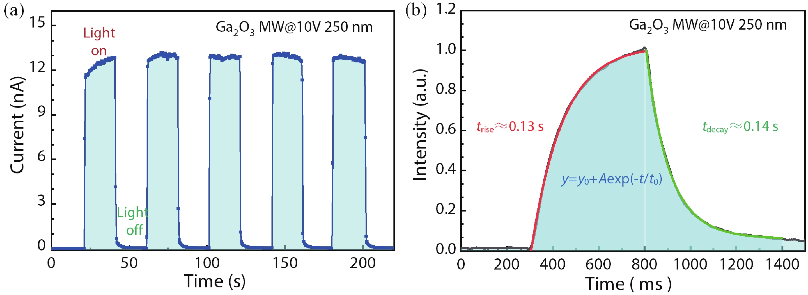
To explore the on/off switching properties of the device in the DUV region, the I–t curves were measured under the wavelength of 250 nm light illumination under a bias voltage of 10 V, as shown in Fig. 5(a). From the figure, it can be found that the current of the device can change obviously with the change of the illumination, and the current exhibits a good stability. In addition, no obvious persistent photoconductivity was observed. As a key parameter for a photodetector, the response speed is tested to investigate the capability of the device to follow a fast-varying optical signal. The light source used in the experiment is a xenon lamp, and the irradiation frequency is controlled by an electronic shutter. The frequency of light signal is set to 2 Hz. Fig. 5(b) shows the variation curve of the current to the pulse light signal. The rise and decay curves are well fitted by the first-order exponential relaxation equation, as follows[13]

| I=I0+Aexp(−t−t1τ), |
where I0 stands for the steady state photocurrent, A is constant, t represents the time, t1 is the fitting constants, and τ is the relaxation time constant. The relaxation time constants for the rise and decay are τr and τd, respectively. The τr and τd for the device obtained using the first-order exponential relaxation equation were fitted to be 0.13 and 0.14 s, respectively. Unlike in most reports, the device does not exhibit obvious persistent photoconductivity. The photoconductive relaxation phenomenon is usually caused by the defect state in the material[35]. The faster response time in this paper is mainly due to the higher crystal quality.
4. Conclusion
In summary, centimeter-long high crystal quality β-Ga2O3 MWs were successfully grown by the CVD method. TEM results show that the microwires are single crystal materials. A β-Ga2O3 MW-based solar-blind MSM photodetector was fabricated, which showed a high detection performance. The responsivity at 240 nm can reach up to 1.2 A/W with a high UV/visible rejection ratio (Rpeak/R400 nm ≈ 5.8 × 10⁵) under 10 V bias. Additionally, the device exhibits a low dark current (78pA) and a fast photoresponse time (τr/τd = 0.13/0.14 s). The excellent performance is attributed to the high crystal quality of the β-Ga2O3 MWs. The results reported in this work show the potential of β-Ga2O3 micro-nano devices in the application of solar-blind ultraviolet detection.
Acknowledgements
This work was supported by the National Key R&D Program of China (Grant No. 2019YFA0705202), and the National Natural Science Foundation of China (Grant Nos. 62274027 and 31701296).
 DownLoad:


 Yuefei Wang:got his PhD degree in 2022 at Harbin Institute of Technology. Then he joined Northeast Normal University as a postdoc. His research focuses on the epitaxial growth of wide band gap semiconductor materials and the preparation of optoelectronic devices
 Bingsheng Li:is currently a professor in Northeast Normal University. He got his PhD degree from University of Chinese Academy of Sciences in 2002. From 2002 to 2012, he carried out research on MBE and PLD in National Institute of Advanced Industrial Science and Technology of Japan, The City College of the City University of New York of USA and University of Tokyo of Japan. In 2012, he joined Harbin Institute of Technology as a full professor. In 2019, he moved to Northeast Normal University where he focuses on the epitaxial growth of oxide and nitride thin films by MOCVD
 DownLoad:


