


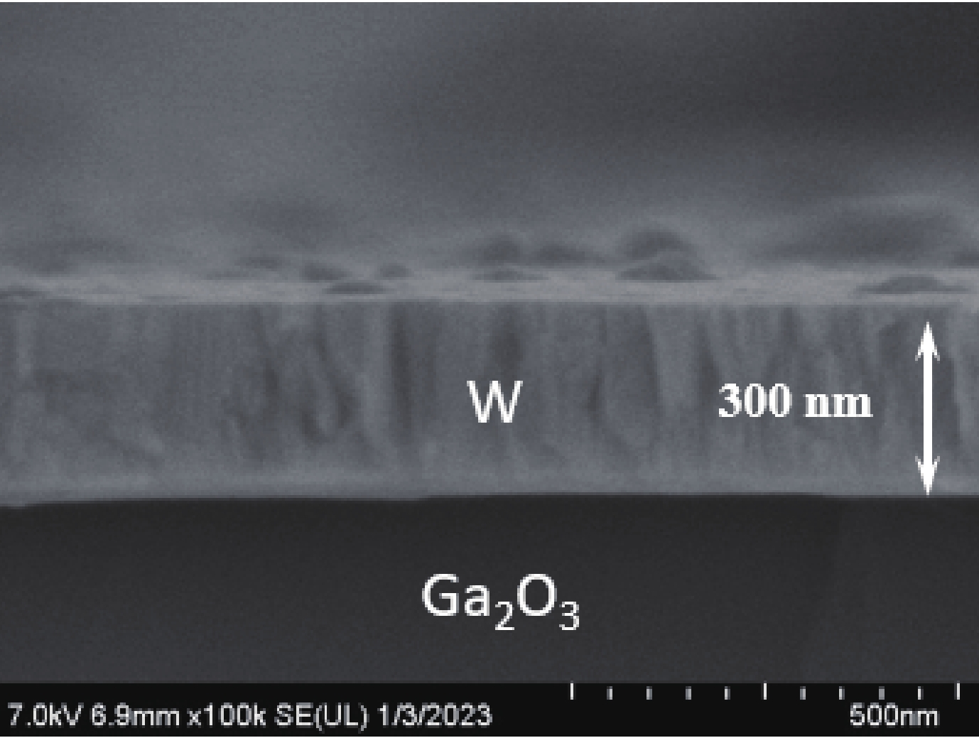
Fig. 1.
An SEM cross section image of W/β-Ga2O3 SBD.
ARTICLES
Madani Labed1, , Ji Young Min1, Amina Ben Slim2, Nouredine Sengouga2, Chowdam Venkata Prasad1, Sinsu Kyoung3 and You Seung Rim1, 4,
Corresponding author: Madani Labed, madani.labed@univ-biskra.dz, madani@sejong.ac.kr; You Seung Rim, youseung@sejong.ac.kr
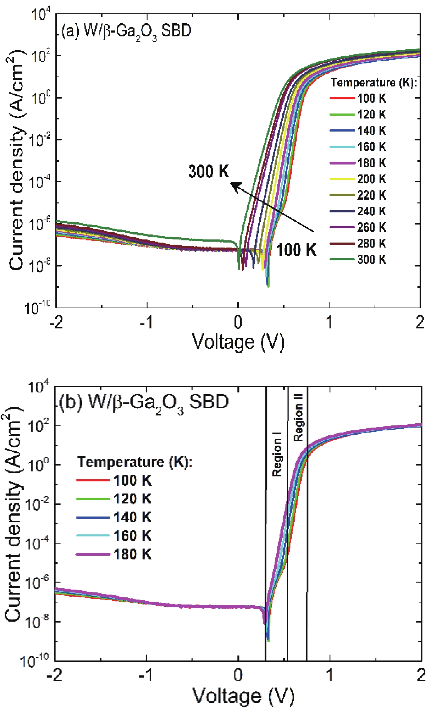
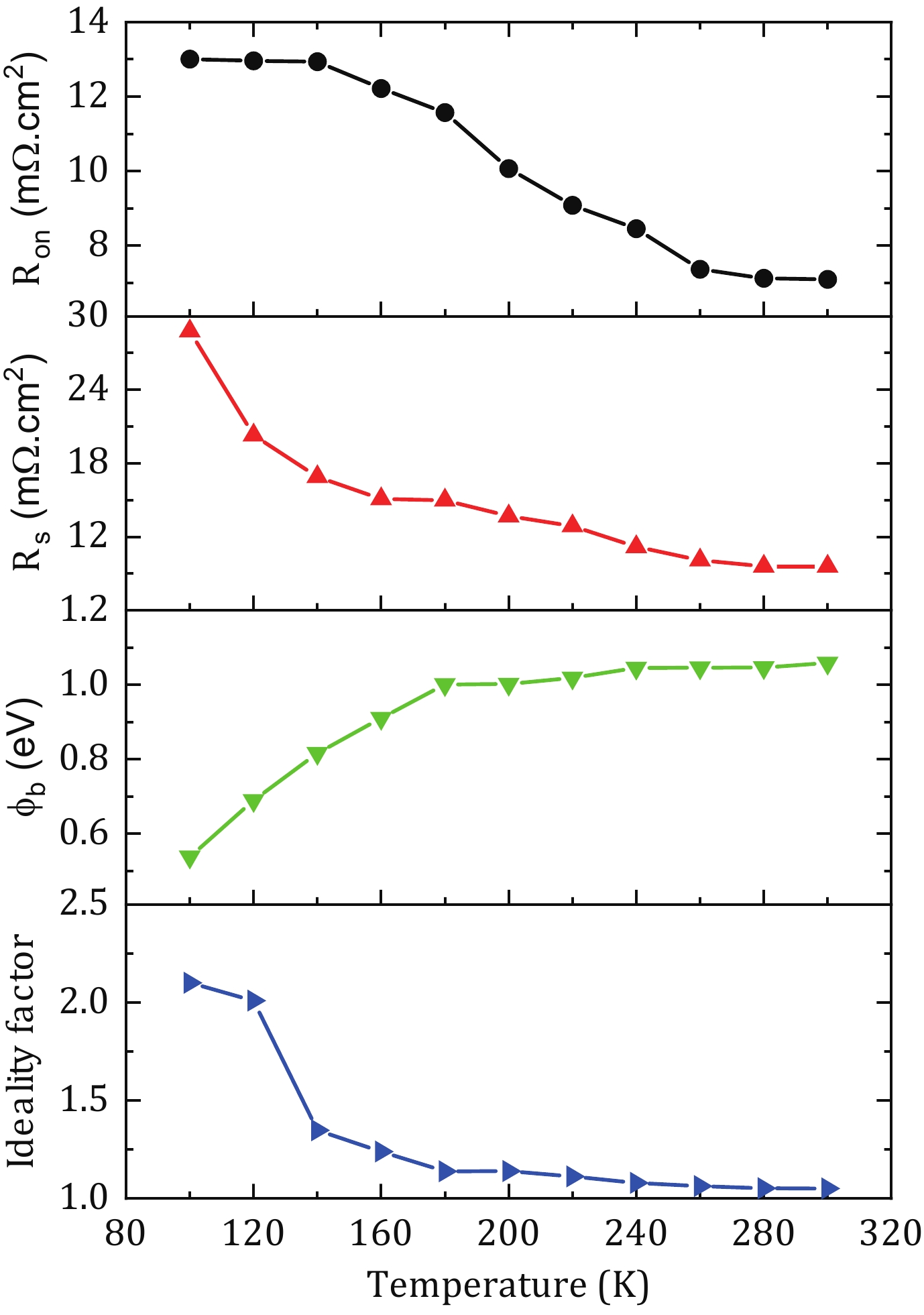
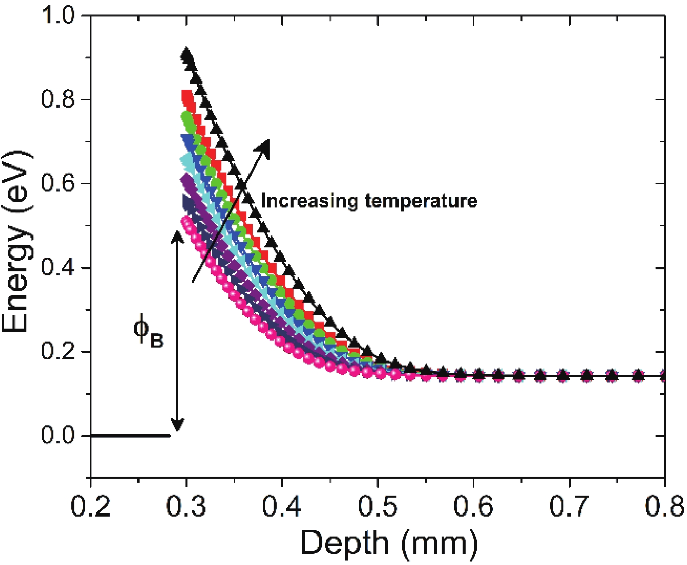
Abstract: In this work, W/β-Ga2O3 Schottky barrier diodes, prepared using a confined magnetic field-based sputtering method, were analyzed at different operation temperatures. Firstly, Schottky barrier height increased with increasing temperature from 100 to 300 K and reached 1.03 eV at room temperature. The ideality factor decreased with increasing temperature and it was higher than 2 at 100 K. This apparent high value was related to the tunneling effect. Secondly, the series and on-resistances decreased with increasing operation temperature. Finally, the interfacial dislocation was extracted from the tunneling current. A high dislocation density was found, which indicates the domination of tunneling through dislocation in the transport mechanism. These findings are evidently helpful in designing better performance devices.
Key words: β-Ga2O3, SBD, SBD paramatters, tungsten, low temperature, tunneling via dislocation
| [1] |
Labed M, Sengouga N, Labed M, et al. Modeling a Ni/β-Ga2O3 Schottky barrier diode deposited by confined magnetic-field-based sputtering. J Phys D, 2021, 54, 115102 doi: 10.1088/1361-6463/abce2c
|
| [2] |
Galazka Z. β-Ga2O3 for wide-bandgap electronics and optoelectronics. Semicond Sci Technol, 2018, 33, 113001 doi: 10.1088/1361-6641/aadf78
|
| [3] |
Galazka Z. Growth of bulk β-Ga2O3 single crystals by the Czochralski method. J Appl Phys, 2022, 131, 31103 doi: 10.1063/5.0076962
|
| [4] |
Pratiyush A S, Muazzam U U, Kumar S, et al. Optical float-zone grown bulk β-Ga2O3-based linear MSM array of UV-C photodetectors. IEEE Photon Technol Lett, 2019, 31, 923 doi: 10.1109/LPT.2019.2913286
|
| [5] |
Hoshikawa K, Ohba E, Kobayashi T, et al. Growth of β-Ga2O3 single crystals using vertical Bridgman method in ambient air. J Cryst Growth, 2016, 447, 36 doi: 10.1016/j.jcrysgro.2016.04.022
|
| [6] |
Bosi M, Seravalli L, Mazzolini P, et al. Thermodynamic and kinetic effects on the nucleation and growth of ε/κ- or β-Ga2O3 by metal–organic vapor phase epitaxy. Cryst Growth Des, 2021, 21, 6393 doi: 10.1021/acs.cgd.1c00863
|
| [7] |
Kyrtsos A, Matsubara M, Bellotti E. On the feasibility of p-type Ga2O3. Appl Phys Lett, 2018, 112, 032108 doi: 10.1063/1.5009423
|
| [8] |
Farzana E, Zhang Z, Paul P K, et al. Influence of metal choice on (010) β-Ga2O3 Schottky diode properties. Appl Phys Lett, 2017, 110, 202102 doi: 10.1063/1.4983610
|
| [9] |
Kim H, Kyoung S, Kang T, et al. Effective surface diffusion of nickel on single crystal β-Ga2O3 for Schottky barrier modulation and high thermal stability. J Mater Chem C, 2019, 7, 10953 doi: 10.1039/C9TC02922B
|
| [10] |
Yao Y, Gangireddy R, Kim J, et al. Electrical behavior of β- Ga2O3 Schottky diodes with different Schottky metals. J Vac Sci Technol B, 2017, 35, 03D113 doi: 10.1116/1.4980042
|
| [11] |
Labed M, Park J H, Meftah A, et al. Low temperature modeling of Ni/β-Ga2O3 Schottky barrier diode interface. ACS Appl Electron Mater, 2021, 3, 3667 doi: 10.1021/acsaelm.1c00647
|
| [12] |
Ravinandan M, Koteswara Rao P, Rajagopal Reddy V. Analysis of the current–voltage characteristics of the Pd/Au Schottky structure on n-type GaN in a wide temperature range. Semicond Sci Technol, 2009, 24, 035004 doi: 10.1088/0268-1242/24/3/035004
|
| [13] |
Parihar U, Ray J, Panchal C J, et al. Influence of temperature on Al/p-CuInAlSe2 thin-film Schottky diodes. Appl Phys A, 2016, 122, 1 doi: 10.1007/s00339-016-0105-9
|
| [14] |
Arslan E, Altındal Ş, Özçelik S, et al. Tunneling current via dislocations in Schottky diodes on AlInN/AlN/GaN heterostructures. Semicond Sci Technol, 2009, 24, 075003 doi: 10.1088/0268-1242/24/7/075003
|
| [15] |
Filali W, Sengouga N, Oussalah S, et al. Characterisation of temperature dependent parameters of multi-quantum well (MQW) Ti/Au/n-AlGaAs/n-GaAs/n-AlGaAs Schottky diodes. Superlattices Microstruct, 2017, 111, 1010 doi: 10.1016/j.spmi.2017.07.059
|
| [16] |
Achard J, Tallaire A, Mille V, et al. Improvement of dislocation density in thick CVD single crystal diamond films by coupling H2/O2 plasma etching and chemo-mechanical or ICP treatment of HPHT substrates. Phys Status Solidi A, 2014, 211, 2264 doi: 10.1002/pssa.201431181
|
| [17] |
Yao Y Z, Ishikawa Y, Sugawara Y. Revelation of dislocations in β-Ga2O3 substrates grown by edge-defined film-fed growth. Phys Status Solidi A, 2020, 217, 1900630 doi: 10.1002/pssa.201900630
|
| [18] |
Kuramata A, Koshi K, Watanabe S, et al. High-quality β-Ga2O3 single crystals grown by edge-defined film-fed growth. Jpn J Appl Phys, 2016, 55, 1202A2 doi: 10.7567/JJAP.55.1202A2
|
| [19] |
Yang T H, Fu H Q, Chen H, et al. Temperature-dependent electrical properties of β-Ga2O3 Schottky barrier diodes on highly doped single-crystal substrates. J Semicond, 2019, 40, 012801 doi: 10.1088/1674-4926/40/1/012801
|
| [20] |
Xian M H, Fares C, Ren F, et al. Effect of thermal annealing for W/β-Ga2O3 Schottky diodes up to 600 °C. J Vac Sci Technol B, 2019, 37, 061201 doi: 10.1116/1.5125006
|
| [21] |
Fares C, Ren F, Pearton S J. Temperature-dependent electrical characteristics of β-Ga2O3 diodes with W Schottky contacts up to 500°C. ECS J Solid State Sci Technol, 2018, 8, Q3007 doi: 10.1149/2.0011907jss
|
| [22] |
Norde H. A modified forward I‐V plot for Schottky diodes with high series resistance. J Appl Phys, 1979, 50, 5052 doi: 10.1063/1.325607
|
| [23] |
Dhimmar J M, Desai H N, Modi B P. The effect of interface states density distribution and series resistance on electrical behaviour of Schottky diode. Mater Today Proc, 2016, 3, 1658 doi: 10.1016/j.matpr.2016.04.056
|
| [24] |
Sekhar Reddy P R, Janardhanam V, Shim K H, et al. Temperature-dependent Schottky barrier parameters of Ni/Au on n-type (001) β-Ga2O3 Schottky barrier diode. Vacuum, 2020, 171, 109012 doi: 10.1016/j.vacuum.2019.109012
|
| [25] |
Higashiwaki M, Sasaki K, Kuramata A, et al. Development of gallium oxide power devices. Phys Status Solidi A, 2014, 211, 21 doi: 10.1002/pssa.201330197
|
| [26] |
Schoeck G, Tiller W A. On dislocation formation by vacancy condensation. Philos Mag A J Theor Exp Appl Phys, 1960, 5, 43 doi: 10.1080/14786436008241199
|
| [27] |
Zade V, Mallesham B, Roy S, et al. Electronic structure of tungsten-doped β-Ga2O3 compounds. ECS J Solid State Sci Technol, 2019, 8, Q3111 doi: 10.1149/2.0121907jss
|
| [28] |
Lee M, Ahn C W, Vu T K O, et al. Current transport mechanism in palladium Schottky contact on Si-based freestanding GaN. Nanomaterials, 2020, 10, E297 doi: 10.3390/nano10020297
|
| [29] |
Belyaev A E, Boltovets N S, Ivanov V N, et al. Mechanism of dislocation-governed charge transport in Schottky diodes based on gallium nitride. Semiconductors, 2008, 42, 689 doi: 10.1134/S1063782608060092
|
| [30] |
Handwerg M, Mitdank R, Galazka Z, et al. Temperature-dependent thermal conductivity in Mg-doped and undoped β-Ga2O3 bulk-crystals. Semicond Sci Technol, 2015, 30, 024006 doi: 10.1088/0268-1242/30/2/024006
|
| [31] |
Ma T C, Chen X H, Kuang Y, et al. On the origin of dislocation generation and annihilation in α-Ga2O3 epilayers on sapphire. Appl Phys Lett, 2019, 115, 182101 doi: 10.1063/1.5120554
|


Article views: 1626 Times PDF downloads: 185 Times Cited by: 0 Times
Received: 26 November 2022 Revised: 05 February 2023 Online: Accepted Manuscript: 22 February 2023Uncorrected proof: 24 February 2023Corrected proof: 12 June 2023Published: 10 July 2023
| Citation: |
Madani Labed, Ji Young Min, Amina Ben Slim, Nouredine Sengouga, Chowdam Venkata Prasad, Sinsu Kyoung, You Seung Rim. Tunneling via surface dislocation in W/β-Ga2O3 Schottky barrier diodes[J]. Journal of Semiconductors, 2023, 44(7): 072801. doi: 10.1088/1674-4926/44/7/072801
****
M Labed, J Y Min, A B Slim, N Sengouga, C V Prasad, S Kyoung, Y S Rim. Tunneling via surface dislocation in W/β-Ga2O3 Schottky barrier diodes[J]. J. Semicond, 2023, 44(7): 072801. doi: 10.1088/1674-4926/44/7/072801

|
 Madani Labed:has obtained his Ph.D. degree in Physics from Biskra University, Algeria in 2022. Currently, he is a postdoctoral researcher at the Department of Intelligent Mechatronics Engineering, Sejong University, South Korea. His current research is focused on the fabrication and simulation of gallium oxide (Ga2O3) based power devices
 Nouredine Sengouga:has obtained his Ph.D. degree in Physical Electronics from Lancaster University. He is a Professor at Biskra University. His research interests are solar cells and other semiconductor devices. He has supervised tens of theses and produced more than 100 publications and conference presentations and a reviewer for several journals
 Chowdam Venkata Prasad:holds a Ph.D. degree in Physics from Sri Venkateswara University, India. Currently, he is a postdoctoral researcher at the Department of Intelligent Mechatronics Engineering, Sejong University, South Korea. His current research is focused on the fabrication of gallium oxide (Ga2O3) based power devices and p–n heterojunctions
 You Seung Rim:received Ph.D. degree from the School of Electrical and Electronic Engineering, Yonsei University, South Korea in 2013. He was a postdoctoral scholar in UCLA from 2013 to 2016. He is currently an associate professor of the Department of Intelligent Mechatronic Engineering at Sejong University in South Korea
| [1] |
Labed M, Sengouga N, Labed M, et al. Modeling a Ni/β-Ga2O3 Schottky barrier diode deposited by confined magnetic-field-based sputtering. J Phys D, 2021, 54, 115102 doi: 10.1088/1361-6463/abce2c
|
| [2] |
Galazka Z. β-Ga2O3 for wide-bandgap electronics and optoelectronics. Semicond Sci Technol, 2018, 33, 113001 doi: 10.1088/1361-6641/aadf78
|
| [3] |
Galazka Z. Growth of bulk β-Ga2O3 single crystals by the Czochralski method. J Appl Phys, 2022, 131, 31103 doi: 10.1063/5.0076962
|
| [4] |
Pratiyush A S, Muazzam U U, Kumar S, et al. Optical float-zone grown bulk β-Ga2O3-based linear MSM array of UV-C photodetectors. IEEE Photon Technol Lett, 2019, 31, 923 doi: 10.1109/LPT.2019.2913286
|
| [5] |
Hoshikawa K, Ohba E, Kobayashi T, et al. Growth of β-Ga2O3 single crystals using vertical Bridgman method in ambient air. J Cryst Growth, 2016, 447, 36 doi: 10.1016/j.jcrysgro.2016.04.022
|
| [6] |
Bosi M, Seravalli L, Mazzolini P, et al. Thermodynamic and kinetic effects on the nucleation and growth of ε/κ- or β-Ga2O3 by metal–organic vapor phase epitaxy. Cryst Growth Des, 2021, 21, 6393 doi: 10.1021/acs.cgd.1c00863
|
| [7] |
Kyrtsos A, Matsubara M, Bellotti E. On the feasibility of p-type Ga2O3. Appl Phys Lett, 2018, 112, 032108 doi: 10.1063/1.5009423
|
| [8] |
Farzana E, Zhang Z, Paul P K, et al. Influence of metal choice on (010) β-Ga2O3 Schottky diode properties. Appl Phys Lett, 2017, 110, 202102 doi: 10.1063/1.4983610
|
| [9] |
Kim H, Kyoung S, Kang T, et al. Effective surface diffusion of nickel on single crystal β-Ga2O3 for Schottky barrier modulation and high thermal stability. J Mater Chem C, 2019, 7, 10953 doi: 10.1039/C9TC02922B
|
| [10] |
Yao Y, Gangireddy R, Kim J, et al. Electrical behavior of β- Ga2O3 Schottky diodes with different Schottky metals. J Vac Sci Technol B, 2017, 35, 03D113 doi: 10.1116/1.4980042
|
| [11] |
Labed M, Park J H, Meftah A, et al. Low temperature modeling of Ni/β-Ga2O3 Schottky barrier diode interface. ACS Appl Electron Mater, 2021, 3, 3667 doi: 10.1021/acsaelm.1c00647
|
| [12] |
Ravinandan M, Koteswara Rao P, Rajagopal Reddy V. Analysis of the current–voltage characteristics of the Pd/Au Schottky structure on n-type GaN in a wide temperature range. Semicond Sci Technol, 2009, 24, 035004 doi: 10.1088/0268-1242/24/3/035004
|
| [13] |
Parihar U, Ray J, Panchal C J, et al. Influence of temperature on Al/p-CuInAlSe2 thin-film Schottky diodes. Appl Phys A, 2016, 122, 1 doi: 10.1007/s00339-016-0105-9
|
| [14] |
Arslan E, Altındal Ş, Özçelik S, et al. Tunneling current via dislocations in Schottky diodes on AlInN/AlN/GaN heterostructures. Semicond Sci Technol, 2009, 24, 075003 doi: 10.1088/0268-1242/24/7/075003
|
| [15] |
Filali W, Sengouga N, Oussalah S, et al. Characterisation of temperature dependent parameters of multi-quantum well (MQW) Ti/Au/n-AlGaAs/n-GaAs/n-AlGaAs Schottky diodes. Superlattices Microstruct, 2017, 111, 1010 doi: 10.1016/j.spmi.2017.07.059
|
| [16] |
Achard J, Tallaire A, Mille V, et al. Improvement of dislocation density in thick CVD single crystal diamond films by coupling H2/O2 plasma etching and chemo-mechanical or ICP treatment of HPHT substrates. Phys Status Solidi A, 2014, 211, 2264 doi: 10.1002/pssa.201431181
|
| [17] |
Yao Y Z, Ishikawa Y, Sugawara Y. Revelation of dislocations in β-Ga2O3 substrates grown by edge-defined film-fed growth. Phys Status Solidi A, 2020, 217, 1900630 doi: 10.1002/pssa.201900630
|
| [18] |
Kuramata A, Koshi K, Watanabe S, et al. High-quality β-Ga2O3 single crystals grown by edge-defined film-fed growth. Jpn J Appl Phys, 2016, 55, 1202A2 doi: 10.7567/JJAP.55.1202A2
|
| [19] |
Yang T H, Fu H Q, Chen H, et al. Temperature-dependent electrical properties of β-Ga2O3 Schottky barrier diodes on highly doped single-crystal substrates. J Semicond, 2019, 40, 012801 doi: 10.1088/1674-4926/40/1/012801
|
| [20] |
Xian M H, Fares C, Ren F, et al. Effect of thermal annealing for W/β-Ga2O3 Schottky diodes up to 600 °C. J Vac Sci Technol B, 2019, 37, 061201 doi: 10.1116/1.5125006
|
| [21] |
Fares C, Ren F, Pearton S J. Temperature-dependent electrical characteristics of β-Ga2O3 diodes with W Schottky contacts up to 500°C. ECS J Solid State Sci Technol, 2018, 8, Q3007 doi: 10.1149/2.0011907jss
|
| [22] |
Norde H. A modified forward I‐V plot for Schottky diodes with high series resistance. J Appl Phys, 1979, 50, 5052 doi: 10.1063/1.325607
|
| [23] |
Dhimmar J M, Desai H N, Modi B P. The effect of interface states density distribution and series resistance on electrical behaviour of Schottky diode. Mater Today Proc, 2016, 3, 1658 doi: 10.1016/j.matpr.2016.04.056
|
| [24] |
Sekhar Reddy P R, Janardhanam V, Shim K H, et al. Temperature-dependent Schottky barrier parameters of Ni/Au on n-type (001) β-Ga2O3 Schottky barrier diode. Vacuum, 2020, 171, 109012 doi: 10.1016/j.vacuum.2019.109012
|
| [25] |
Higashiwaki M, Sasaki K, Kuramata A, et al. Development of gallium oxide power devices. Phys Status Solidi A, 2014, 211, 21 doi: 10.1002/pssa.201330197
|
| [26] |
Schoeck G, Tiller W A. On dislocation formation by vacancy condensation. Philos Mag A J Theor Exp Appl Phys, 1960, 5, 43 doi: 10.1080/14786436008241199
|
| [27] |
Zade V, Mallesham B, Roy S, et al. Electronic structure of tungsten-doped β-Ga2O3 compounds. ECS J Solid State Sci Technol, 2019, 8, Q3111 doi: 10.1149/2.0121907jss
|
| [28] |
Lee M, Ahn C W, Vu T K O, et al. Current transport mechanism in palladium Schottky contact on Si-based freestanding GaN. Nanomaterials, 2020, 10, E297 doi: 10.3390/nano10020297
|
| [29] |
Belyaev A E, Boltovets N S, Ivanov V N, et al. Mechanism of dislocation-governed charge transport in Schottky diodes based on gallium nitride. Semiconductors, 2008, 42, 689 doi: 10.1134/S1063782608060092
|
| [30] |
Handwerg M, Mitdank R, Galazka Z, et al. Temperature-dependent thermal conductivity in Mg-doped and undoped β-Ga2O3 bulk-crystals. Semicond Sci Technol, 2015, 30, 024006 doi: 10.1088/0268-1242/30/2/024006
|
| [31] |
Ma T C, Chen X H, Kuang Y, et al. On the origin of dislocation generation and annihilation in α-Ga2O3 epilayers on sapphire. Appl Phys Lett, 2019, 115, 182101 doi: 10.1063/1.5120554
|

 WeChat ID
Journal of Semiconductors © 2017 All Rights Reserved 京ICP备05085259号-2

 DownLoad:

