


Fig. 1.
(Color online) Cross-section of considered GaN/AlGaN HEMT transistor.
ARTICLES
Amgad A. Al-Saman1, 2, Eugeny A. Ryndin3, Xinchuan Zhang2, Yi Pei2, and Fujiang Lin1,
Corresponding author: Yi Pei, yi.pei@dynax-semi.com; Fujiang Lin, linfj@ustc.edu.cn
Abstract: A physics-based analytical expression that predicts the charge, electrical field and potential distributions along the gated region of the GaN HEMT channel has been developed. Unlike the gradual channel approximation (GCA), the proposed model considers the non-uniform variation of the concentration under the gated region as a function of terminal applied voltages. In addition, the model can capture the influence of mobility and channel temperature on the charge distribution trend. The comparison with the hydrodynamic (HD) numerical simulation showed a high agreement of the proposed model with numerical data for different bias conditions considering the self-heating and quantization of the electron concentration. The analytical nature of the model allows us to reduce the computational and time cost of the simulation. Also, it can be used as a core expression to develop a complete physics-based transistor Ⅳ model without GCA limitation.
Key words: AlGaN/GaN (HEMTs), 2DEG, charge distribution, electron mobility, hydrodynamic model, channel temperature
| [1] |
Al-Saman A A, Pei Y, Ryndin E A, et al. Accurate temperature estimation for each gate of GaN HEMT with n-gate fingers. IEEE Trans Electron Devices, 2020, 67, 3577 doi: 10.1109/TED.2020.3012116
|
| [2] |
Hoo Teo K, Zhang Y H, Chowdhury N, et al. Emerging GaN technologies for power, RF, digital, and quantum computing applications: Recent advances and prospects. J Appl Phys, 2021, 130, 160902 doi: 10.1063/5.0061555
|
| [3] |
Meneghini M, De Santi C, Abid I, et al. GaN-based power devices: Physics, reliability, and perspectives. J Appl Phys, 2021, 130, 181101 doi: 10.1063/5.0061354
|
| [4] |
Zhu G Q, Chang C, Xu Y H, et al. A small-signal model extraction and optimization method for AlGaN/GaN HEMT up to 110 GHz. 2019 IEEE International Conference on Integrated Circuits, Technologies and Applications (ICTA), 2020, 111 doi: 10.1109/ICTA48799.2019.9012880
|
| [5] |
Zhu G Q, Chang C, Xu Y H, et al. A millimeter-wave scalable small-signal modeling approach based on FW-EM for AlGaN/GaN HEMT up to 110 GHz. Microw Opt Technol Lett, 2021, 63, 2145 doi: 10.1002/mop.32404
|
| [6] |
Al-Saman A A, Ryndin E A, Pei Y, et al. An estimation of 2DEG density for GaN HEMT using analytical equation considering the charge conservation low. Solid State Electron, 2022, 188, 108209 doi: 10.1016/j.sse.2021.108209
|
| [7] |
Anbuselvan N, Amudhalakshmi P, Mohankumar N. Analytical modeling of 2DEG and 2DHG charge balancing in quaternary Al0.42In0.03Ga0.55N/Al0.3In0.7NAl0.42In0.03Ga0.55N/Al0.3In0.7N HEMTs. J Comput Electron, 2018, 17, 1191 doi: 10.1007/s10825-018-1164-2
|
| [8] |
Jena K, Swain R, Lenka T R. Physics-based mathematical model of 2DEG sheet charge density and DC characteristics of AlInN/AlN/GaN MOSHEMT. Int J Numer Model Electron Netw Devices Fields, 2017, 30, e2117 doi: 10.1002/jnm.2117
|
| [9] |
Khandelwal S, Chauhan Y S, Fjeldly T A. Analytical modeling of surface-potential and intrinsic charges in AlGaN/GaN HEMT devices. IEEE Trans Electron Devices, 2012, 59, 2856 doi: 10.1109/TED.2012.2209654
|
| [10] |
Khandelwal S, Goyal N, Fjeldly T A. A physics-based analytical model for 2DEG charge density in AlGaN/GaN HEMT devices. IEEE Trans Electron Devices, 2011, 58, 3622 doi: 10.1109/TED.2011.2161314
|
| [11] |
Ashok A, Vasileska D, Hartin O L, et al. Electrothermal Monte Carlo simulation of GaN HEMTs including electron–electron interactions. IEEE Trans Electron Devices, 2010, 57, 562 doi: 10.1109/TED.2009.2038585
|
| [12] |
Si J, Wei J, Chen W J, et al. Electric field distribution around drain-side gate edge in AlGaN/GaN HEMTs: Analytical approach. IEEE Trans Electron Devices, 2013, 60, 3223 doi: 10.1109/TED.2013.2272055
|
| [13] |
Sadi T, Kelsall R W, Pilgrim N J. Investigation of self-heating effects in submicrometer GaN/AlGaN HEMTs using an electrothermal Monte Carlo method. IEEE Trans Electron Devices, 2006, 53, 2892 doi: 10.1109/TED.2006.885099
|
| [14] |
Yamakawa S, Goodnick S, Aboud S, et al. Quantum corrected full-band cellular Monte Carlo simulation of AlGaN/GaN HEMTs. J Comput Electron, 2004, 3, 299 doi: 10.1007/s10825-004-7065-6
|
| [15] |
Minetto A, Deutschmann B, Modolo N, et al. Hot-electron effects in AlGaN/GaN HEMTs under semi-ON DC stress. IEEE Trans Electron Devices, 2020, 67, 4602 doi: 10.1109/TED.2020.3025983
|
| [16] |
Ryndin E A, Al-Saman A. A novel approach to model high-speed microelectronic switch on the basis of hydrodynamic approximation. International Conference on Micro- and Nano-Electronics 2018, 2019, 128 doi: 10.1117/12.2521711
|
| [17] |
Wang X D, Hu W D, Chen X S, et al. The study of self-heating and hot-electron effects for AlGaN/GaN double-channel HEMTs. IEEE Trans Electron Devices, 2012, 59, 1393 doi: 10.1109/TED.2012.2188634
|
| [18] |
Asgari A, Kalafi M, Faraone L. A quasi-two-dimensional charge transport model of AlGaN/GaN high electron mobility transistors (HEMTs). Phys E, 2005, 28, 491 doi: 10.1016/j.physe.2005.05.054
|
| [19] |
Khandelwal S, Chauhan Y S, Fjeldly T A, et al. ASM GaN: Industry standard model for GaN RF and power devices—Part 1: DC, CV, and RF model. IEEE Trans Electron Devices, 2019, 66, 80 doi: 10.1109/TED.2018.2867874
|
| [20] |
Ali Albahrani S, Mahajan D, Hodges J, et al. ASM GaN: Industry standard model for GaN RF and power devices—Part-II: Modeling of charge trapping. IEEE Trans Electron Devices, 2019, 66, 87 doi: 10.1109/TED.2018.2868261
|
| [21] |
Radhakrishna U, Choi P, Grajal J, et al. Study of RF-circuit linearity performance of GaN HEMT technology using the MVSG compact device model. 2016 IEEE International Electron Devices Meeting (IEDM), 2017, 3.7.1 doi: doi.org/10.1117/12.2521711
|
| [22] |
Radhakrishna U, Imada T, Palacios T, et al. MIT virtual source GaNFET-high voltage (MVSG-HV) model: A physics based compact model for HV-GaN HEMTs. Phys Status Solidi C, 2014, 11, 848 doi: 10.1002/pssc.201300392
|
| [23] |
Khandelwal S, Yigletu F M, Iñiguez B, et al. A charge-based capacitance model for AlGaAs/GaAs HEMTs. Solid State Electron, 2013, 82, 38 doi: 10.1016/j.sse.2013.01.017
|
| [24] |
Palankovski V, Quay R. Analysis and Simulation of Heterostructure Devices. Vienna: Springer Vienna, 2004
|
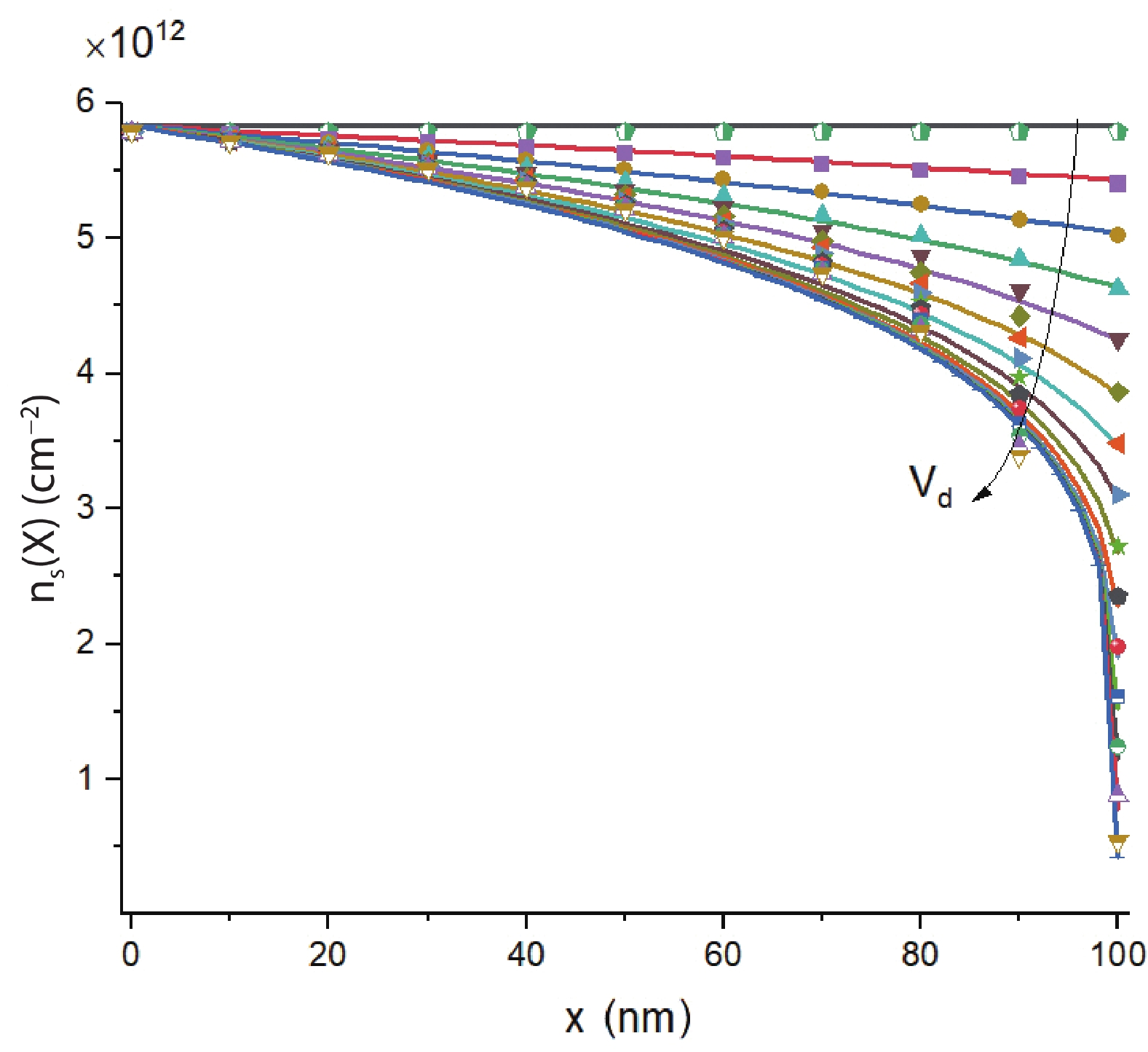
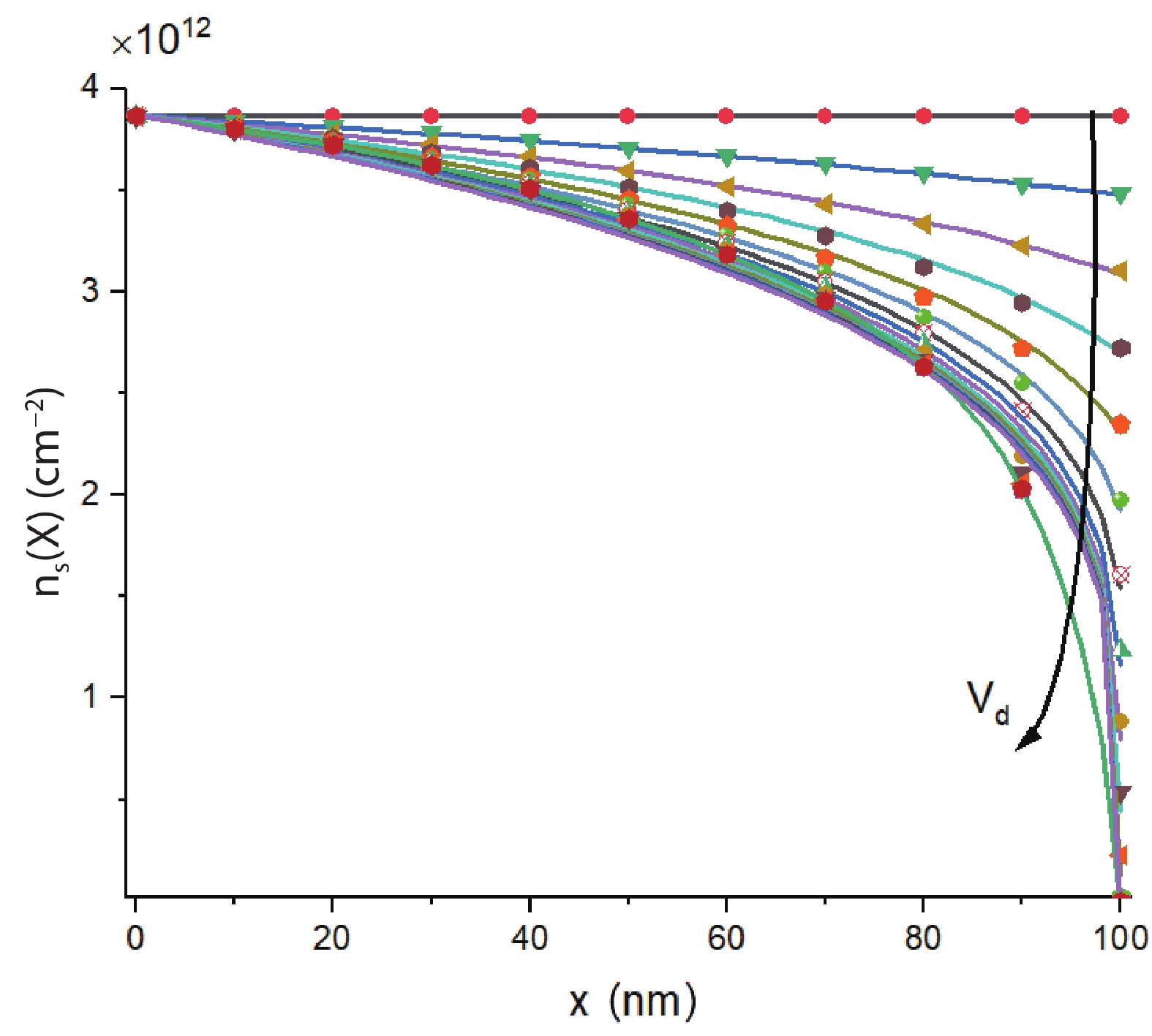
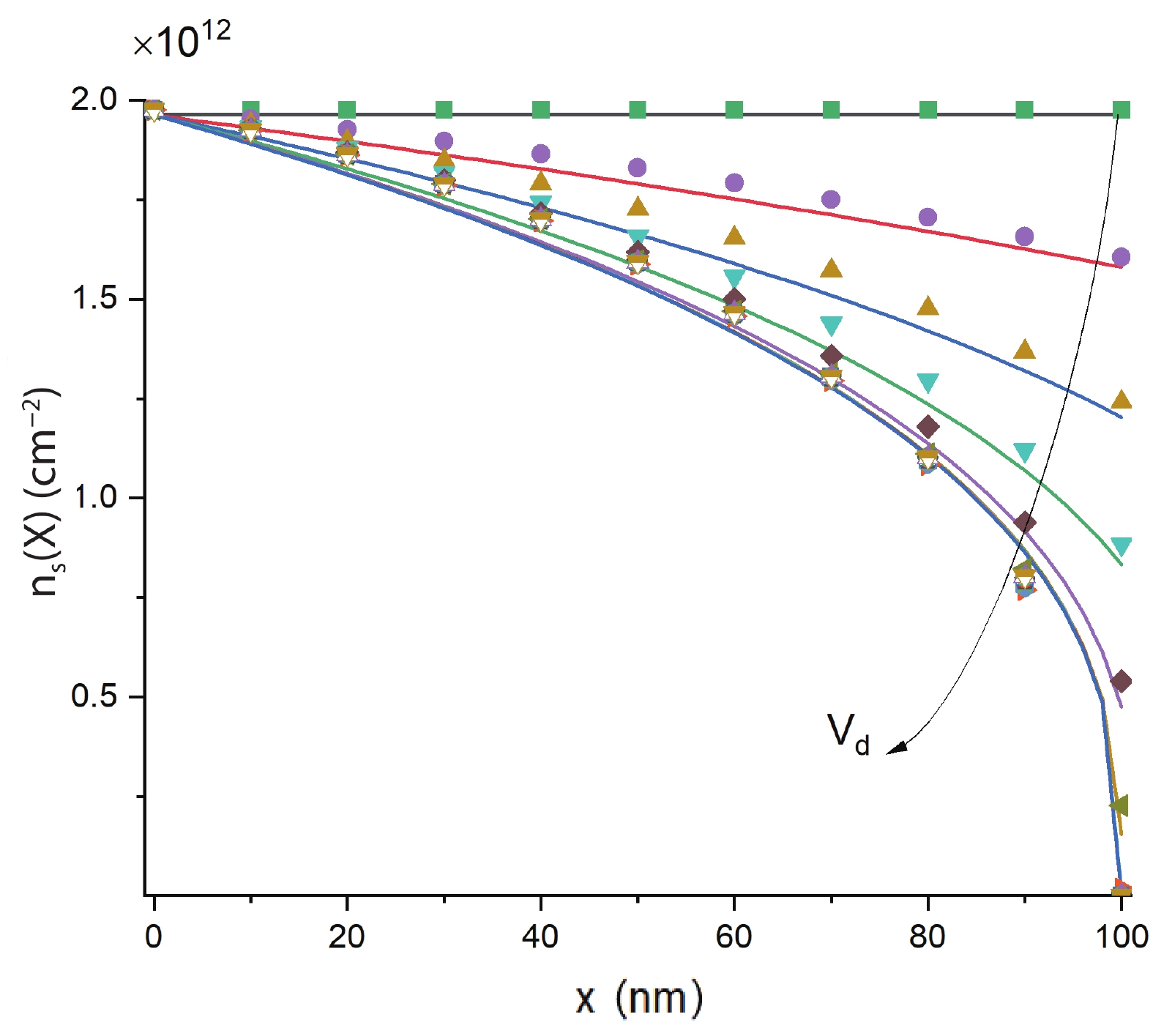
Table 1. Geometrical and simulation parameters of considered GaN/AlGaN HEMT transistor.
| Parameter | Symble | Value | Parameter | Symble | Value |
| Threshold voltage | Voff | –2.1 V | Mobility | µ | 2000 cm2/(V·s) |
| Gate length | Lg | 0.1 µm | Saturation velocity | vs | 2.9 × 10⁵ m/s |
| Gate width | Wg | 4 × 30 µm | Exp. parameter | γ1 | 2.12 × 10⁻¹² |
| Barrier thickness | d | 30 nm | Exp. parameter | γ2 | 3.73 × 10⁻¹² |
| Channel thikness | Wch | 1 µm | Controlling parameters | η1, η2 | 0.5 × 10⁻² |
| Substrate thickness | Ws | 100 µm | Controlling parameter | $a$1 | 1 |
| AlGaN dielectric cons | ε | 10.66 × 10⁻¹¹ F/m | Controlling parameter | $a$2 | 5 |
 DownLoad: CSV
| [1] |
Al-Saman A A, Pei Y, Ryndin E A, et al. Accurate temperature estimation for each gate of GaN HEMT with n-gate fingers. IEEE Trans Electron Devices, 2020, 67, 3577 doi: 10.1109/TED.2020.3012116
|
| [2] |
Hoo Teo K, Zhang Y H, Chowdhury N, et al. Emerging GaN technologies for power, RF, digital, and quantum computing applications: Recent advances and prospects. J Appl Phys, 2021, 130, 160902 doi: 10.1063/5.0061555
|
| [3] |
Meneghini M, De Santi C, Abid I, et al. GaN-based power devices: Physics, reliability, and perspectives. J Appl Phys, 2021, 130, 181101 doi: 10.1063/5.0061354
|
| [4] |
Zhu G Q, Chang C, Xu Y H, et al. A small-signal model extraction and optimization method for AlGaN/GaN HEMT up to 110 GHz. 2019 IEEE International Conference on Integrated Circuits, Technologies and Applications (ICTA), 2020, 111 doi: 10.1109/ICTA48799.2019.9012880
|
| [5] |
Zhu G Q, Chang C, Xu Y H, et al. A millimeter-wave scalable small-signal modeling approach based on FW-EM for AlGaN/GaN HEMT up to 110 GHz. Microw Opt Technol Lett, 2021, 63, 2145 doi: 10.1002/mop.32404
|
| [6] |
Al-Saman A A, Ryndin E A, Pei Y, et al. An estimation of 2DEG density for GaN HEMT using analytical equation considering the charge conservation low. Solid State Electron, 2022, 188, 108209 doi: 10.1016/j.sse.2021.108209
|
| [7] |
Anbuselvan N, Amudhalakshmi P, Mohankumar N. Analytical modeling of 2DEG and 2DHG charge balancing in quaternary Al0.42In0.03Ga0.55N/Al0.3In0.7NAl0.42In0.03Ga0.55N/Al0.3In0.7N HEMTs. J Comput Electron, 2018, 17, 1191 doi: 10.1007/s10825-018-1164-2
|
| [8] |
Jena K, Swain R, Lenka T R. Physics-based mathematical model of 2DEG sheet charge density and DC characteristics of AlInN/AlN/GaN MOSHEMT. Int J Numer Model Electron Netw Devices Fields, 2017, 30, e2117 doi: 10.1002/jnm.2117
|
| [9] |
Khandelwal S, Chauhan Y S, Fjeldly T A. Analytical modeling of surface-potential and intrinsic charges in AlGaN/GaN HEMT devices. IEEE Trans Electron Devices, 2012, 59, 2856 doi: 10.1109/TED.2012.2209654
|
| [10] |
Khandelwal S, Goyal N, Fjeldly T A. A physics-based analytical model for 2DEG charge density in AlGaN/GaN HEMT devices. IEEE Trans Electron Devices, 2011, 58, 3622 doi: 10.1109/TED.2011.2161314
|
| [11] |
Ashok A, Vasileska D, Hartin O L, et al. Electrothermal Monte Carlo simulation of GaN HEMTs including electron–electron interactions. IEEE Trans Electron Devices, 2010, 57, 562 doi: 10.1109/TED.2009.2038585
|
| [12] |
Si J, Wei J, Chen W J, et al. Electric field distribution around drain-side gate edge in AlGaN/GaN HEMTs: Analytical approach. IEEE Trans Electron Devices, 2013, 60, 3223 doi: 10.1109/TED.2013.2272055
|
| [13] |
Sadi T, Kelsall R W, Pilgrim N J. Investigation of self-heating effects in submicrometer GaN/AlGaN HEMTs using an electrothermal Monte Carlo method. IEEE Trans Electron Devices, 2006, 53, 2892 doi: 10.1109/TED.2006.885099
|
| [14] |
Yamakawa S, Goodnick S, Aboud S, et al. Quantum corrected full-band cellular Monte Carlo simulation of AlGaN/GaN HEMTs. J Comput Electron, 2004, 3, 299 doi: 10.1007/s10825-004-7065-6
|
| [15] |
Minetto A, Deutschmann B, Modolo N, et al. Hot-electron effects in AlGaN/GaN HEMTs under semi-ON DC stress. IEEE Trans Electron Devices, 2020, 67, 4602 doi: 10.1109/TED.2020.3025983
|
| [16] |
Ryndin E A, Al-Saman A. A novel approach to model high-speed microelectronic switch on the basis of hydrodynamic approximation. International Conference on Micro- and Nano-Electronics 2018, 2019, 128 doi: 10.1117/12.2521711
|
| [17] |
Wang X D, Hu W D, Chen X S, et al. The study of self-heating and hot-electron effects for AlGaN/GaN double-channel HEMTs. IEEE Trans Electron Devices, 2012, 59, 1393 doi: 10.1109/TED.2012.2188634
|
| [18] |
Asgari A, Kalafi M, Faraone L. A quasi-two-dimensional charge transport model of AlGaN/GaN high electron mobility transistors (HEMTs). Phys E, 2005, 28, 491 doi: 10.1016/j.physe.2005.05.054
|
| [19] |
Khandelwal S, Chauhan Y S, Fjeldly T A, et al. ASM GaN: Industry standard model for GaN RF and power devices—Part 1: DC, CV, and RF model. IEEE Trans Electron Devices, 2019, 66, 80 doi: 10.1109/TED.2018.2867874
|
| [20] |
Ali Albahrani S, Mahajan D, Hodges J, et al. ASM GaN: Industry standard model for GaN RF and power devices—Part-II: Modeling of charge trapping. IEEE Trans Electron Devices, 2019, 66, 87 doi: 10.1109/TED.2018.2868261
|
| [21] |
Radhakrishna U, Choi P, Grajal J, et al. Study of RF-circuit linearity performance of GaN HEMT technology using the MVSG compact device model. 2016 IEEE International Electron Devices Meeting (IEDM), 2017, 3.7.1 doi: doi.org/10.1117/12.2521711
|
| [22] |
Radhakrishna U, Imada T, Palacios T, et al. MIT virtual source GaNFET-high voltage (MVSG-HV) model: A physics based compact model for HV-GaN HEMTs. Phys Status Solidi C, 2014, 11, 848 doi: 10.1002/pssc.201300392
|
| [23] |
Khandelwal S, Yigletu F M, Iñiguez B, et al. A charge-based capacitance model for AlGaAs/GaAs HEMTs. Solid State Electron, 2013, 82, 38 doi: 10.1016/j.sse.2013.01.017
|
| [24] |
Palankovski V, Quay R. Analysis and Simulation of Heterostructure Devices. Vienna: Springer Vienna, 2004
|


Article views: 1226 Times PDF downloads: 120 Times Cited by: 0 Times
Received: 31 October 2022 Revised: 27 January 2023 Online: Uncorrected proof: 08 March 2023Accepted Manuscript: 08 March 2023Published: 10 August 2023
| Citation: |
Amgad A. Al-Saman, Eugeny A. Ryndin, Xinchuan Zhang, Yi Pei, Fujiang Lin. Analytical model of non-uniform charge distribution within the gated region of GaN HEMTs[J]. Journal of Semiconductors, 2023, 44(8): 082802. doi: 10.1088/1674-4926/44/8/082802
****
A A Al-Saman, E A Ryndin, X C Zhang, Y Pei, F J Lin. Analytical model of non-uniform charge distribution within the gated region of GaN HEMTs[J]. J. Semicond, 2023, 44(8): 082802. doi: 10.1088/1674-4926/44/8/082802

|
 Amgad A. Al-Saman:was born in Yemen, in 1988. He received the B.Sc. degree (with honours) in electronics and microelectronics and M.S. degree in electronics and nanoelectronics from Southern Federal University, Russia, in 2012 and 2014, respectively. From 2014 to 2018 he was a junior researcher at Scientific and Educational Center "Nanotechnology" at Southern Federal University. At the end of 2018 he was certified researcher. In 2019 he joined the University of Science and Technology of China, Hefei as a Ph.D student. Currently, he is a visiting scholar at Dynax Semiconductor Inc. He has authored multiple international journal and conference publication. His current research interests include physical modelling of semiconductor devices
 Eugeny A. Ryndin:was born in Gorlovka, Donetsk region, USSR in 1968. He graduated from the Radiotechnical Institute, Taganrog, Russia in 1992. He received the Ph.D degree in electrical engineering in 1997 and the Doctor of Science degree in 2008. From 1997 to 2004, he was an Associate Professor with the Electronic Apparatuses Design Department, Taganrog State University of Radioengineering. From 2004 to 2008, he was a Senior Researcher with the Southern Scientific Center, Russian Academy of Science, Rostov-on-Don. From 2008 to 2019, he was a Professor with the Institute of Nanotechnologies, Electronics and Electronic Equipment Engineering, Southern Federal University, Taganrog. Since 2019, he has been a Professor with the Micro- and Nanoelectronics Department, Saint Petersburg Electrotechnical University "LETI", Saint Petersburg. His research interests include micro- and nanoelectronic elements development and numerical modeling, MEMS development and VLSI design
 Yi Pei:received the B.S degree in Electrical Engineering from Peking University, Beijing, China, in 2004, the M.S and Ph.D degrees in Electrical Engineering from University of Santa Barbara, U.S.A, in 2005 and 2009, respectively. He is currently the V.P. of technology, in charge of GaN product design, cutting edge GaN technology development and I.P. strategy. His research interests include microwave and millimeter wave GaN electronics design and modeling, GaN power electronics design and application, and Ⅲ-N semiconductor processing technology development. He is the author or coauthor of more than 100 journal and conference papers. He also holds more than 150 granted patents and patent applications
 Fujiang Lin:received the B.S. and M.S. degrees from the University of Science and Technology of China (USTC), Hefei, China, in 1982 and 1984, respectively, and the Dr.-Ing. degree from the University of Kassel, Germany, in 1993, all in electrical engineering. His research interest is in the development of CMOS as a cost-effective technology platform for 60-GHz band millimeter-wave SoC, as well as millimeter wave therapy for healthcare applications. He is initiator and co-organizer of international workshops and short courses at APMC99, SPIE00, ISAP06, and IMS07. Dr. Lin was the recipient of the 1998 Innovator Award presented by EDN Asia Magazine. He has authored or coauthored over 150 scientific papers. He holds over 50 patents
| [1] |
Al-Saman A A, Pei Y, Ryndin E A, et al. Accurate temperature estimation for each gate of GaN HEMT with n-gate fingers. IEEE Trans Electron Devices, 2020, 67, 3577 doi: 10.1109/TED.2020.3012116
|
| [2] |
Hoo Teo K, Zhang Y H, Chowdhury N, et al. Emerging GaN technologies for power, RF, digital, and quantum computing applications: Recent advances and prospects. J Appl Phys, 2021, 130, 160902 doi: 10.1063/5.0061555
|
| [3] |
Meneghini M, De Santi C, Abid I, et al. GaN-based power devices: Physics, reliability, and perspectives. J Appl Phys, 2021, 130, 181101 doi: 10.1063/5.0061354
|
| [4] |
Zhu G Q, Chang C, Xu Y H, et al. A small-signal model extraction and optimization method for AlGaN/GaN HEMT up to 110 GHz. 2019 IEEE International Conference on Integrated Circuits, Technologies and Applications (ICTA), 2020, 111 doi: 10.1109/ICTA48799.2019.9012880
|
| [5] |
Zhu G Q, Chang C, Xu Y H, et al. A millimeter-wave scalable small-signal modeling approach based on FW-EM for AlGaN/GaN HEMT up to 110 GHz. Microw Opt Technol Lett, 2021, 63, 2145 doi: 10.1002/mop.32404
|
| [6] |
Al-Saman A A, Ryndin E A, Pei Y, et al. An estimation of 2DEG density for GaN HEMT using analytical equation considering the charge conservation low. Solid State Electron, 2022, 188, 108209 doi: 10.1016/j.sse.2021.108209
|
| [7] |
Anbuselvan N, Amudhalakshmi P, Mohankumar N. Analytical modeling of 2DEG and 2DHG charge balancing in quaternary Al0.42In0.03Ga0.55N/Al0.3In0.7NAl0.42In0.03Ga0.55N/Al0.3In0.7N HEMTs. J Comput Electron, 2018, 17, 1191 doi: 10.1007/s10825-018-1164-2
|
| [8] |
Jena K, Swain R, Lenka T R. Physics-based mathematical model of 2DEG sheet charge density and DC characteristics of AlInN/AlN/GaN MOSHEMT. Int J Numer Model Electron Netw Devices Fields, 2017, 30, e2117 doi: 10.1002/jnm.2117
|
| [9] |
Khandelwal S, Chauhan Y S, Fjeldly T A. Analytical modeling of surface-potential and intrinsic charges in AlGaN/GaN HEMT devices. IEEE Trans Electron Devices, 2012, 59, 2856 doi: 10.1109/TED.2012.2209654
|
| [10] |
Khandelwal S, Goyal N, Fjeldly T A. A physics-based analytical model for 2DEG charge density in AlGaN/GaN HEMT devices. IEEE Trans Electron Devices, 2011, 58, 3622 doi: 10.1109/TED.2011.2161314
|
| [11] |
Ashok A, Vasileska D, Hartin O L, et al. Electrothermal Monte Carlo simulation of GaN HEMTs including electron–electron interactions. IEEE Trans Electron Devices, 2010, 57, 562 doi: 10.1109/TED.2009.2038585
|
| [12] |
Si J, Wei J, Chen W J, et al. Electric field distribution around drain-side gate edge in AlGaN/GaN HEMTs: Analytical approach. IEEE Trans Electron Devices, 2013, 60, 3223 doi: 10.1109/TED.2013.2272055
|
| [13] |
Sadi T, Kelsall R W, Pilgrim N J. Investigation of self-heating effects in submicrometer GaN/AlGaN HEMTs using an electrothermal Monte Carlo method. IEEE Trans Electron Devices, 2006, 53, 2892 doi: 10.1109/TED.2006.885099
|
| [14] |
Yamakawa S, Goodnick S, Aboud S, et al. Quantum corrected full-band cellular Monte Carlo simulation of AlGaN/GaN HEMTs. J Comput Electron, 2004, 3, 299 doi: 10.1007/s10825-004-7065-6
|
| [15] |
Minetto A, Deutschmann B, Modolo N, et al. Hot-electron effects in AlGaN/GaN HEMTs under semi-ON DC stress. IEEE Trans Electron Devices, 2020, 67, 4602 doi: 10.1109/TED.2020.3025983
|
| [16] |
Ryndin E A, Al-Saman A. A novel approach to model high-speed microelectronic switch on the basis of hydrodynamic approximation. International Conference on Micro- and Nano-Electronics 2018, 2019, 128 doi: 10.1117/12.2521711
|
| [17] |
Wang X D, Hu W D, Chen X S, et al. The study of self-heating and hot-electron effects for AlGaN/GaN double-channel HEMTs. IEEE Trans Electron Devices, 2012, 59, 1393 doi: 10.1109/TED.2012.2188634
|
| [18] |
Asgari A, Kalafi M, Faraone L. A quasi-two-dimensional charge transport model of AlGaN/GaN high electron mobility transistors (HEMTs). Phys E, 2005, 28, 491 doi: 10.1016/j.physe.2005.05.054
|
| [19] |
Khandelwal S, Chauhan Y S, Fjeldly T A, et al. ASM GaN: Industry standard model for GaN RF and power devices—Part 1: DC, CV, and RF model. IEEE Trans Electron Devices, 2019, 66, 80 doi: 10.1109/TED.2018.2867874
|
| [20] |
Ali Albahrani S, Mahajan D, Hodges J, et al. ASM GaN: Industry standard model for GaN RF and power devices—Part-II: Modeling of charge trapping. IEEE Trans Electron Devices, 2019, 66, 87 doi: 10.1109/TED.2018.2868261
|
| [21] |
Radhakrishna U, Choi P, Grajal J, et al. Study of RF-circuit linearity performance of GaN HEMT technology using the MVSG compact device model. 2016 IEEE International Electron Devices Meeting (IEDM), 2017, 3.7.1 doi: doi.org/10.1117/12.2521711
|
| [22] |
Radhakrishna U, Imada T, Palacios T, et al. MIT virtual source GaNFET-high voltage (MVSG-HV) model: A physics based compact model for HV-GaN HEMTs. Phys Status Solidi C, 2014, 11, 848 doi: 10.1002/pssc.201300392
|
| [23] |
Khandelwal S, Yigletu F M, Iñiguez B, et al. A charge-based capacitance model for AlGaAs/GaAs HEMTs. Solid State Electron, 2013, 82, 38 doi: 10.1016/j.sse.2013.01.017
|
| [24] |
Palankovski V, Quay R. Analysis and Simulation of Heterostructure Devices. Vienna: Springer Vienna, 2004
|

 WeChat ID
Journal of Semiconductors © 2017 All Rights Reserved 京ICP备05085259号-2


