Processing math: 100%
J. Semicond. > 2023, Volume 44 > Issue 8 > 082901

ARTICLES

Terahertz phononic crystal in plasmonic nanocavity

Zhenyao Li1, 2, Haonan Chang1, 2, Jia-Min Lai1, 2, Feilong Song1, 2, Qifeng Yao3, Hanqing Liu1, 2, Haiqiao Ni1, 2, 4, Zhichuan Niu1, 2, 4 and Jun Zhang1, 2, 3,

+ Author Affiliations

 Corresponding author: Jun Zhang, zhangjwill@semi.ac.cn

DOI: 10.1088/1674-4926/44/8/082901

PDF

Turn off MathJax

Abstract: Interaction between photons and phonons in cavity optomechanical systems provides a new toolbox for quantum information technologies. A GaAs/AlAs pillar multi-optical mode microcavity optomechanical structure can obtain phonons with ultra-high frequency (~THz). However, the optical field cannot be effectively restricted when the diameter of the GaAs/AlAs pillar microcavity decreases below the diffraction limit of light. Here, we design a system that combines Ag nanocavity with GaAs/AlAs phononic superlattices, where phonons with the frequency of 4.2 THz can be confined in a pillar with ~4 nm diameter. The Qc/V reaches 0.22 nm−3, which is ~80 times that of the photonic crystal (PhC) nanobeam and ~100 times that of the hybrid point-defect PhC bowtie plasmonic nanocavity, where Qc is optical quality factor and V is mode volume. The optomechanical single-photon coupling strength can reach 12 MHz, which is an order of magnitude larger than that of the PhC nanobeam. In addition, the mechanical zero-point fluctuation amplitude is 85 fm and the efficient mass is 0.27 zg, which is much smaller than the PhC nanobeam. The phononic superlattice-Ag nanocavity optomechanical devices hold great potential for applications in the field of integrated quantum optomechanics, quantum information, and terahertz-light transducer.

Key words: Optomechanicsphononic crystalAg plasmonic nanocavityconfinementcoupling

The field of cavity optomechanics explores the interaction between electromagnetic radiation and nanomechanical or micromechanical motion[1]. Cavity optomechanics has important applications in precision measurement, regulation of macroscopic quantum properties of matter, quantum memory, and so on[2-6]. To observe quantum effects on a micromechanical element, it should first be cooled to the quantum ground state. An ultrahigh frequency THz GaAs/AlAs pillar multi-optical mode microcavity optomechanical structure has been proposed[7]. The high phonon frequency range that is obtained might even allow devices to be prepared in the quantum mechanical ground state of motion at liquid-nitrogen temperatures. Under blue-detuned driving, the photon-phonon interaction produces Stokes sidebands that correspond to phonon emission, due to an energy exchange between photons and phonons. In this process, the effective Hamiltonian has the form of two-mode squeezing, which is useful for the heralded generation of non-classical mechanical states or amplification of the mechanical motion[8]. For cavity optomechanics, to manipulate the quantum states precisely, enhance the coupling strength[9-11], reduce the thermal effect of laser, and achieve integration, it is important to reduce the volume of the optical coupling region. However, large mode volumes of GaAs/AlAs pillar multi-optical mode microcavity are hard to further reduce due to the diffraction limitation of light[9, 12, 13]. Plasmonic nano-antennas or plasmonic nano-cavities have the properties of localized surface plasmon resonances, so they can confine light into volumes far below the diffraction limit[14]. In addition, the GaAs/AlAs phononic superlattices have high adjustability, which can be used to design a narrow phononic crystal cavity. The combination of GaAs/AlAs superlattices phononic crystal and plasmonic nano-cavities is expected to reduce the mode volume and enhance the single-photon optomechanical coupling strength.

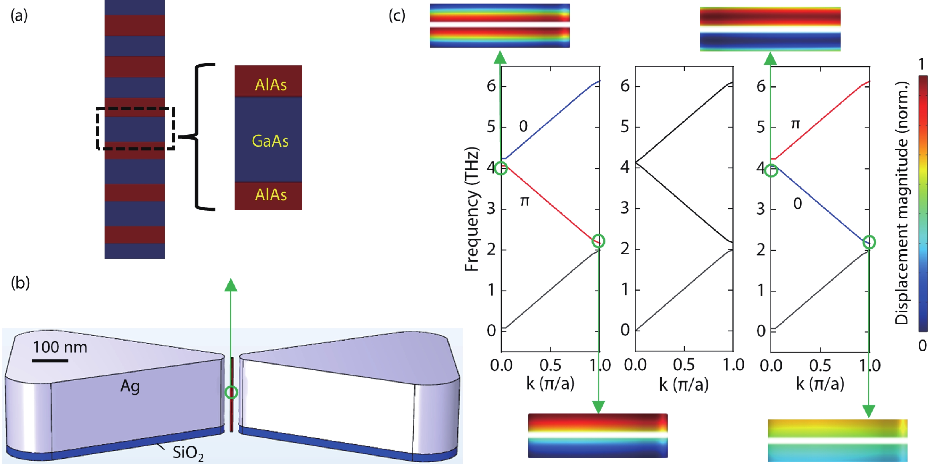
Here, we design a topological terahertz GaAs/AlAs phononic superlattice in a plasmonic nanocavity, where silver (Ag) plasmonic nanocavity is combined with GaAs/AlAs phononic crystal superlattices, as shown in Figs. 1(a) and 1(b). The phononic crystal cavity is designed to confine phonons in a range of around 4 nm in diameter. The plasmonic nanocavity with bowtie type put the phononic crystal superlattices post in the middle, which makes the optical field covered by the phonon range effective. The characteristic wavelength of the plasmonic nanocavity is designed to be 1550 nm, which has low loss in quartz fiber and has important applications in optical communication. The optical quality factor Qc and optical mode volume V of cavity can attain 238 and 5 × 10⁻⁷ (λ/n)3, respectively, and Qc/V achieves 8.4 × 10⁸ (λ/n)−3, where λ is the wavelength of the light and n is the refractive index. The optomechanical single-photon coupling strength reaches 12 MHz, which is an order of magnitude higher than the conventional photonic crystal (PhC) nanobeam dielectric cavity.

Fig. 1.  (Color online) (a) Scheme of a phononic superlattice structure and its unit cell. The thickness of the upper part GaAs (AlAs) layer is different from the lower part. (b) The system composed of GaAs/AlAs phononic superlattice and bowtie Ag nanocavity with SiO2 underneath. (c) The band inversion of GaAs/AlAs phononic superlattice δ is negative, zero, and positive from the left-hand to right-hand in the figure, respectively. The Zak phase of the middle band in each figure changes from 0 to π.

To obtain a phonon state, GaAs and AlAs occupy different proportions in the upper and lower superlattices. At a designed frequency f0, the total acoustic path length of the unit cell is set to a half wavelength of phonons λ/2, i.e., the thicknesses d of the two layers obeys dGaAsvGaAs+dAlAsvAlAs=12f0[15], where v is the velocity of phonons. When a phonon traverses in both layers of the cell at f0, the accumulated phase shift is π. To describe how the overall acoustic path length is distributed between the two materials, a parameter 1<δ<1 is defined. Keeping f0 constant, the thicknesses of the GaAs and AlAs layers are dGaAs=vGaAs4f0(1+δ) and dAlAs=vAlAs4f0(1δ)[15], respectively. In Fig. 1(c), we show three phonon bands corresponding to cases where δ is negative, zero, and positive and band inversion can be found. Take the middle band in each figure of Fig. 1(c) as an example: when the Zak phase is π, the band is nontrivial topological and the symmetry of modes between the center and the edge of the Brillouin region is different; when the Zak phase is 0, the band is trivial topological and the symmetry of modes between the center and the edge of the Brillouin region is the same. In this case, the reflection phases ϕright and ϕleft of the upper and lower individual superlattices have to add up to an integer multiple of 2π and a stationary wave is formed. Then, a topological interface state confined between two concatenated superlattices is constructed for frequencies that fall into a bandgap for both phononic crystals. Adjusting the thickness of the superlattices, the frequency of phonons can achieve around 4 THz, which helps to realize ground-state quantum states at about 200 K. The key of phononic state confinement is to confine the topological interface phononic state in a superlattice pillar with diameters on the order of the wavelength of phonons. By reducing the diameter of the superlattices, we can limit phonons to the region of the nanometer scale.

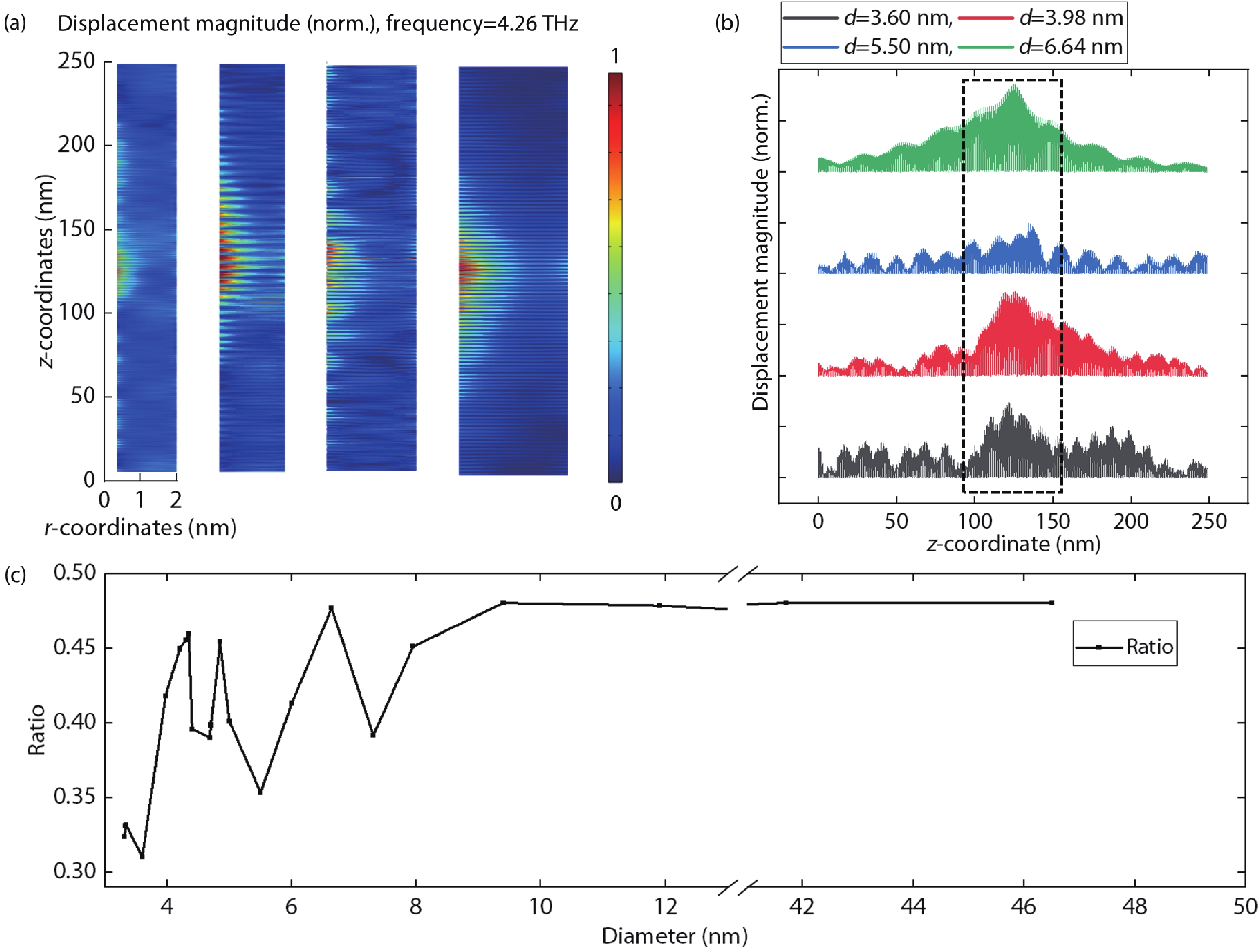
The decrease of the diameter of the superlattices pillar has a limit, which is related to the wavelength of phonons. We know that the length of superlattices cannot be shorter than the half wavelength of phonons. Therefore, shorter wavelengths are better to confine the phonons. This is another reason why the eigenfrequency of phononic superlattices is designed as high as the minimum thickness of GaAs and the AlAs layer can be grown by molecular beam epitaxy (MBE). It should be noted that the velocity of sound is different in GaAs and AlAs, so only when the superlattice pillar diameter takes a specific value, the topological phonon states exist stably at the interface between two phononic crystals. Here, the distribution of displacement magnitude is calculated by the finite element method (FEM). The thickness of the upper and lower half GaAs/AlAs units is 0.5121/0.7412 nm and 0.6260/0.6064 nm, respectively, and the number of periods is 100. The density of GaAs and AlAs are set as 5370 and 3810 kg/m3. Fig. 2(a) shows the distribution of the amplitude of the phonons at 4.26 THz with different superlattice pillar diameters. Fig. 2(b) further quantitatively shows the distribution of phonon amplitudes along the axial direction. There are phonons vibrating in various directions. It can be seen when diameter d takes 3.98 and 6.64 nm, there is the obvious phononic state, which distributes in the interface of phononic superlattices. While diameter d takes 3.60 nm and 5.50 nm, confinement of phonons is not good, which means that there is no stable interface state. Fig. 2(c) shows the change of ratio when the diameter takes from 3.32 to 46.50 nm. We can see when the diameter is smaller than 10 nm, the ratio periodically obtains the maximum value, and when the diameter is larger than 10 nm, the ratio is stable, which means that the interface phononic states can exist at almost every size. Therefore, when we need to confine phonons within a range that is as small as possible, the smallest diameter is 3.98 nm. When the requirement of phonon restriction is more than 10 nm, the diameter of superlattices can be arbitrarily set according to actual needs.

Fig. 2.  (Color online) (a) The amplitude distribution of the topological interface phonons at 4.26 THz when the diameter of the superlattices pillar is at 3.60, 3.98, 5.50, and 6.64 nm. (b) The amplitude of the phonons depending on the coordinate in the axial direction (z-axis) at 4.26 THz. The phonon amplitudes at the z-axis coordinate 95–155 nm are framed in the black dotted box, where the phonon integrated amplitude is denoted as i1. In addition, the overall phonon integrated amplitude is i2. We define the ratio as i1/i2 to reflect the confinement of phonons under phononic states with different diameters. (c) The ratio depending on the diameter from 3.32 to 46.50 nm.

We also calculate mechanical zero-point fluctuation amplitude xzpf and effective mass meff of 4.26 THz phonon modes at 3.98 nm diameter. xzpf is expressed as xzpf=/2meffωm, where ωm is the angular mechanical frequency. The xzpf is 85 fm and the meff is 0.27 zg, which is much smaller than PhC nanobeam[16-18] and photonic distributed Bragg reflection (DBR) phononic superlattices[7] with micron level diameter, as shown in Table 1. The mechanical quality-factor Qm is 2494, which is higher than photonic DBR/phononic superlattices[7]. The f × Qm is around 10 PHz, which is much larger than kBT/h with kB being the Boltzmann and h the Planck constant at T = 300 K. This is expected to achieve quantum ground state at room temperature[19]. Furthermore, if the superlattice pillar is isolated from the substrate to eliminate dissipation, such as suspended by optical tweezers, then Qm can theoretically reach ~1016 and mechanical damping rate can be reduced to ~1 mHz, reaching the minimum of the current optomechanical experiment[19].

Table 1.  The comparison of phononic frequency, Qm, xzpf, and meff between different optomechanical system.
SystemPhC nanobeam[18]Photonic DBR / Phononic superlattices[7]*This work
Phononic
frequency
~5 GHz4.2 THz4.2 THz
Qm~4.9 × 10¹⁰~3002494
xzpf (fm)~0.10.04785
meff136 fg0.92 fg0.27 zg
* We use the structure of the reference and recalculate the relevant parameters. The same is true for the data in Tables 2 and 3.
DownLoad: CSV  | Show Table

To realize optomechanical coupling, an optical cavity that is capable of confining light and combining with phononic superlattices is required. In the design of the light cavity, the optical quality factor Qc and mode volume V are important parameters, which represent the spectral energy density and spatial energy density of the optical microcavities. They quantitatively describe how long in time the cavity can store light and how small in space the cavity can localize light[20-22]. The light-matter interaction strength is proportional to Qc/V, so the figure of merit Qc/V is introduced as a basic measure to evaluate the ability of optical cavities in enhancing light-matter interaction[20, 22]. The core task is how to achieve high Qc/V for strong light-matter interaction[14].

For our system, on the one hand, the Qc/V of the optical cavity needs to be large enough to achieve the enhancement of the optical field. On the other hand, the light field needs to be sufficient to cover the phonon field. We chose light with a wavelength of 1550 nanometers, which has important applications in light communications[17, 23-28]. However, the photonic DBR cannot confine 1550 nm light to the size of the phononic superlattice pillar with 4 nm diameter. Plasmonic nano-cavities or plasmonic nano-antennas have the properties of localized surface plasmon resonances, so they can confine light into ultra-small volumes far below the diffraction limit of light[14]. For metal plasmonic nano-cavities, the high value of Qc/V can be realized due to the ultra-small V[14, 29, 30]. We use Ag commonly used to construct the optical cavity at 1550 nm wavelength of light[23-25]. The schematic of light field distribution is shown in Fig. 3(a) calculated by FEM, where the light is confined to the metal cavity and covers the whole phononic superlattices well. The linewidth of cavity resonance is around 0.8 THz, which is smaller than the eigenfrequency of phononic crystal. This means that the optomechanical system satisfies the resolved sideband condition.

Fig. 3.  (Color online) (a) The distribution of optical field in Ag nanocavity. The middle, upper and right parts are views in x-z, x-y and y-z directions, respectively. Ex, Ey, and Ez are the components of the electric field in the x, y, and z directions, respectively. (b) and (c) The variation of Qc, V, and Qc/V with Dx.

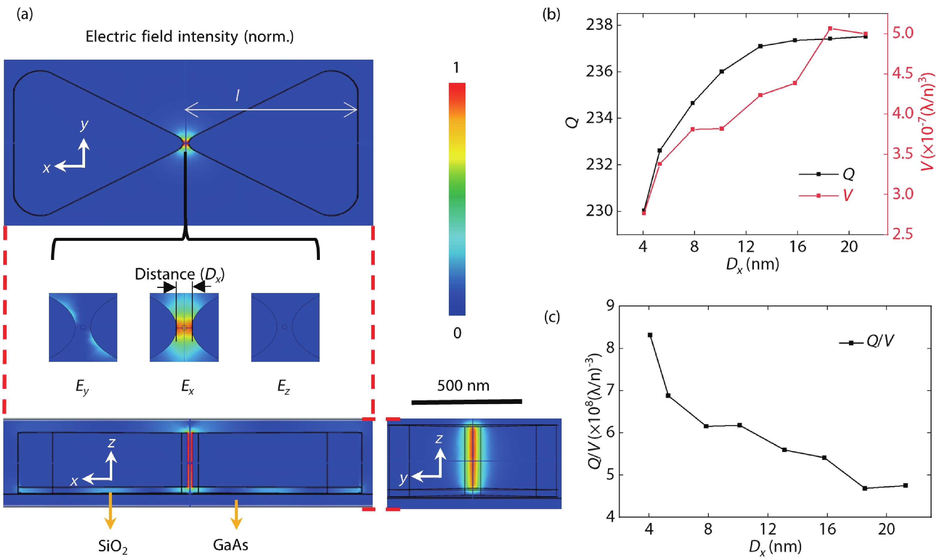
The Ag nanocavity can carry phononic crystal superlattices with different sizes, as shown in Fig. 3(a). The distribution of different components of electric field is shown, where Ex is the strongest. For the nanocavity, the various parameters depending on the distance (Dx) of two parts of the Ag bowtie need to be investigated. In the changing of the Dx, an important point is to keep its characteristic resonant frequency at 1550 nm, so it is necessary to change the lateral size (l) of the nanocavity at the same time. We find when the characteristic wavelength of the nanocavity is kept at 1550 nm, the relationship between Dx and l satisfies |l|=550+7.66|Dx|0.156|Dx|2. The Qc and V depending on Dx are shown in Fig. 3(b). When Dx changes from 4.07 to 21.28 nm, Qc and V both increase. Qc changes from 230 to 238, which is higher than reported plasmonic nanocavity[14], and V changes from 2.8 to 5.0 × 10⁻⁷ (λ/n)3, which is six orders of magnitude smaller than the PhC nanobeam[16-18], on the same order of magnitude as the pico-cavity[10], and five orders of magnitude smaller than the hybrid point-defect PhC and bowtie plasmonic nanocavity[9, 14], as shown in Table 2. In the simulation, the area covered by the light field is mostly air, so n is approximately 1. Even if the optical field is mainly occupied by GaAs/AlAs superlattices, V is about 7 × 10⁻⁶ (λ/n)3. From Fig. 3(c), Qc/V is negatively correlated with Dx. Limited by the size of the phononic superlattices, the nanocavity Dx can be as small as 4.07 nm, and the corresponding Qc/V reaches 8.4 × 10⁸ (λ/n)−3, which is enhanced more than 80 times with respect to the PhC nanobeam[16-18] and more than 100 times with respect to the hybrid photonic-plasmonic nanocavity[9, 14], as shown in Table 2.

Table 2.  Comparison of cavity wavelength, Qc, V, and Qc/V between different cavities.
SystemPhC
nanobeam[17, 31]
Pico-
cavities[10]
Hybrid photonic-plasmonic
nano-cavity[9, 14]
Photonic DBR / Phononic superlattices[7]*This work
Cavity wavelength (nm)~1550[17, 31]633131015501550
Optical Q-factor~106[17]9.8 × 10445238
Mode volume V (λ/n)3~0.1[31]~1.2 × 10−71.2 × 10−262.8 × 10⁻⁷
Qc/V (108 (λ/n)-3)~0.10.0847.5 × 10−88.4
DownLoad: CSV  | Show Table

To verify the enhancement of the optomechanical interaction, we calculate the optomechanical single-photon coupling strength g of the system. In the optomechanical cavity, the injected photons inside the cavity generate the radiation-pressure forces, including gradient forces, scattering forces, and thermal effects[1], which make a slight structural deformation around the center of the cavity. In turn, the optical field is modified by the moving dielectric boundary and the change of refractive index caused by the strain field, which is called the photo-elastic effect[32]. To quantify the interaction between photons and phonons, g is defined as[1, 17, 31]

g=xzpfdωo/dα, (1)

where α is the amplitude of the mechanical displacement field and ω0 is the angular frequency of the optical mode. dωo/dα, calculated by first-order electromagnetic perturbation theory, demonstrates the strength of optomechanical transductions. Given the contribution of the moving dielectric boundary and the photo-elastic effect, the total optomechanical single-photon coupling strength can be written as g=gmb+gpe. The moving boundary contribution is given by[17, 31]

gmb=ωo2(Qˆn)(ΔϵE2Δϵ1D2)dSEDdVxzpf, (2)

where ˆn is the outward facing surface normal, Q is the normalized mechanical vector displacement field (max[|Q|]=1), D is the electric displacement field, E is the electric field, the subscripts and indicate the field components parallel and perpendicular to the surface, respectively. ε is the material permittivity, Δε=εmaterialεair, and Δε1=ε1materialε1air (here, the material is GaAs or AlAs.). The photo-elastic contribution is written as[17, 31]

gpe=ωo2E|εα|EEDdVxzpf. (3)

εα is given by dεdα=ε(pSε0)ε, where S is the strain tensor and p is the rank-four photo-elastic tensor. For calculation, E|εα|E is written in terms of components:

E|εα|E=ε0n4[2Re{ExEy}p44Sxy+2Re{ExEz}p44Sxz+2Re{EyEz}p44Syz+|Ex|2(p11Sxx+p12(Syy+Szz))+|Ey|2(p11Syy+p12(Sxx+Szz))+|Ez|2(p11Szz+p12(Sxx+Syy)]dV. (4)

The photo-elastic coefficients for GaAs are taken as (p11, p12, p44) = (−0.165, −0.140, (p11p12)/2)[33-35]. We neglect the contributions of the AlAs layers to the g because the photo-elastic effect of the GaAs layers will be dominant over those of AlAs[36]. The photoelastic contribution depends mainly on the coupling of the electric field and the phonon field which are non-perpendicular. When the Ex direction is the strongest and Ey and Ez can be negligible, the phonon modes vibrating perpendicular to the x axis cannot be effectively coupled with the light field in gpe, and the breathing phonon modes are fully coupled.

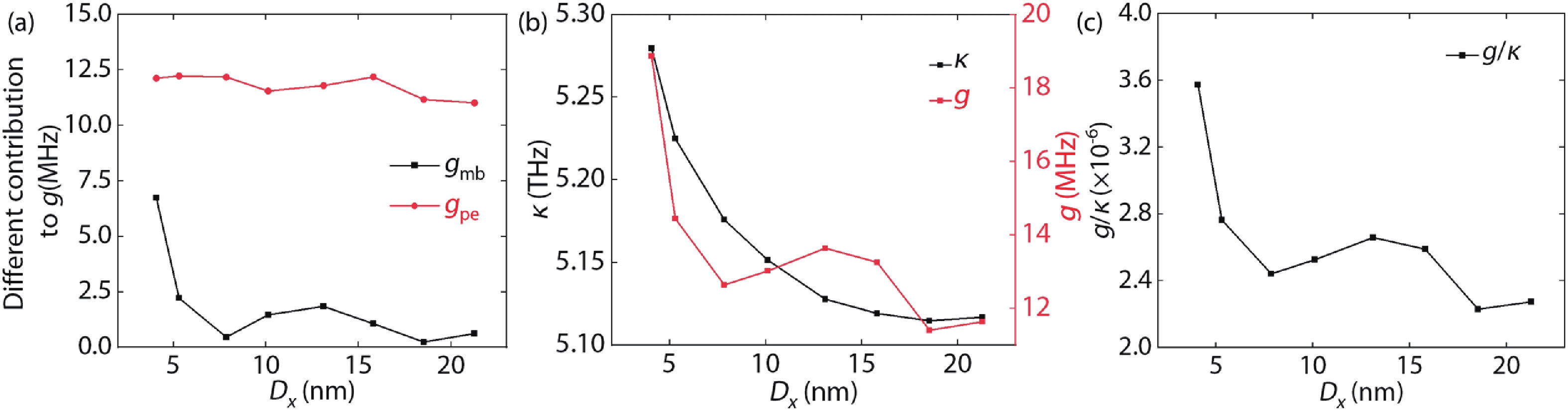
The influence of distance on gpe and gmb is shown as Fig. 4(a). Both gpe and gmb decrease as distance Dx increases and the photo-elastic effect contributes more to the coupling strength. In Fig. 4(b), we see g change from 12 to 18 MHz when Dx decreases and increases sharply at a small distance, which is one order of magnitude higher than PhC nanobeam[16-18], as shown in Table 3. This verifies that the plasmonic cavity greatly increased light intensity in a small area and lower Dx raises higher enhancement. Moreover, gpe is mainly decided by the overlap of strain and optical fields from Eq. (3). Because the distribution of the optical field is larger than the strain field, the coverage of the optical field to the phonon field is the key to ensure sufficient coupling strength. When the full coverage is satisfied, the smaller the distance, the smaller the volume of the light field mode. On the one hand, the light field has a higher enhancement; on the other hand, the overlap of the light field and the phonon field is improved, resulting in a higher g. In addition, the decay rate κ depending on Dx is calculated by κ=ω0Q also shown in Fig. 4(b). Fig. 4(c) shows the relationship between g/κ and Dx. When Dx is small, g/κ is large and κ is larger than g obviously, which means that the system has relatively high coupling strength[1] but it has not yet reached strong coupling and our calculation method can be used.

Fig. 4.  (Color online) Optomechanical single-photon coupling strength (a) gpe and gmb depending on Dx. (b) g and κ depending on Dx. (c) g/κ depending on Dx.
Table 3.  Comparison of phononic frequency, gmb, gpe, and g between different optomechanical systems.
SystemPhC
nanobeam[18, 31]
Photonic DBR /
Phononic
superlattices[7]*
This work
Phononic frequency~5 GHz4.2 THz4.2 THz
gmb (kHz)~100[31]400600
gpe (MHz)~1[31]3.211
g (MHz)~1[18, 31]3.612
DownLoad: CSV  | Show Table

In this paper, we propose a hybrid plasmonic nanocavity and topological terahertz optomechanical system combining topological GaAs/AlAs phononic crystal superlattices vibrated at eigen phonon frequency 4.2 THz with Ag plasmonic cavity resonant at 1550 nm. By adjusting the diameter of the superlattice pillar, the phonons are confined with a diameter of ~4 nm and xzpf and meff can achieve 85 fm and 0.27 zg, respectively. Ag plasmonic cavity is designed to confine the optical field and improve the overlap of the optical and mechanical modes. We get V ~2.8 × 10⁻⁷ (λ/n)3 and Qc/V ~8.4 × 10⁸ (λ/n)−3, which is ~80 times that of the PhC nanobeam and ~100 times that of the hybrid photonic-plasmonic nanocavity. As a result, an optomechanical single-photon coupling strength as high as 12 MHz is obtained, which is the highest among the reported optomechanical crystal cavities in the case of non-strong coupling. The proposed phononic-plasmonic nano-cavity provides a new platform to reduce the mode volume and improve the optomechanical single-photon coupling strength, which holds great potential for applications in the field of integrated quantum optomechanics, quantum information, and terahertz-light transducer.

J. Z. acknowledges National Natural Science Foundation of China (12074371), CAS Interdisciplinary Innovation Team, Strategic Priority Research Program of Chinese Academy of Sciences (XDB28000000). and Key-Area Research and Development Program of Guangdong Province (Grant No. 2018B030329001).


[1]
Aspelmeyer M, Kippenberg T J, Marquardt F. Cavity optomechanics. Rev Mod Phys, 2014, 86, 1391 doi: 10.1103/RevModPhys.86.1391
[2]
Abbott B P, Abbott R, Abbott T D, et al. Observation of gravitational waves from a binary black hole merger. Phys Rev Lett, 2016, 116, 061102 doi: 10.1103/PhysRevLett.116.061102
[3]
Wallucks A, Marinković I, Hensen B, et al. A quantum memory at telecom wavelengths. Nat Phys, 2020, 16, 772 doi: 10.1038/s41567-020-0891-z
[4]
Kuruma K, Pingault B, Chia C, et al. Coupling of a single tin-vacancy center to a photonic crystal cavity in diamond. Appl Phys Lett, 2021, 118, 230601 doi: 10.1063/5.0051675
[5]
Barzanjeh S, Xuereb A, Gröblacher S, et al. Optomechanics for quantum technologies. Nat Phys, 2022, 18, 15 doi: 10.1038/s41567-021-01402-0
[6]
Zhou Z Q, Cui Y, Tan P H, et al. Optical and electrical properties of two-dimensional anisotropic materials. J Semicond, 2019, 40, 061001 doi: 10.1088/1674-4926/40/6/061001
[7]
Chang H N, Li Z Y, Lou W K, et al. Terahertz cavity optomechanics using a topological nanophononic superlattice. Nanoscale, 2022, 14, 13046 doi: 10.1039/D2NR03376C
[8]
Meenehan S M. Cavity optomechanics at Millikelvin temperatures. PhD Dissertation, California Institute of Technology, 2015 (in USA)
[9]
Zhang H Y, Liu Y C, Wang C Y, et al. Hybrid photonic-plasmonic nano-cavity with ultra-high Q/V. Opt Lett, 2020, 45, 4794 doi: 10.1364/OL.402781
[10]
Benz F, Schmidt M K, Dreismann A, et al. Single-molecule optomechanics in picocavities. Science, 2016, 354, 726 doi: 10.1126/science.aah5243
[11]
Su R, Ghosh S, Wang J, et al. Observation of exciton polariton condensation in a perovskite lattice at room temperature. Nat Phys, 2020, 16, 301 doi: 10.1038/s41567-019-0764-5
[12]
Spillane S M, Kippenberg T J, Vahala K J. Ultralow-threshold Raman laser using a spherical dielectric microcavity. Nature, 2002, 415, 621 doi: 10.1038/415621a
[13]
Armani D K, Kippenberg T J, Spillane S M, et al. Ultra-high-Q toroid microcavity on a chip. Nature, 2003, 421, 925 doi: 10.1038/nature01371
[14]
Zhang H Y, Zhao W, Liu Y T, et al. Photonic-plasmonic hybrid microcavities: Physics and applications. Chin Phys B, 2021, 30, 117801 doi: 10.1088/1674-1056/ac0db3
[15]
Esmann M, Lamberti F R, Senellart P, et al. Topological nanophononic states by band inversion. Phys Rev B, 2018, 97, 155422 doi: 10.1103/PhysRevB.97.155422
[16]
Chan J, Alegre T P, Safavi-Naeini A H, et al. Laser cooling of a nanomechanical oscillator into its quantum ground state. Nature, 2011, 478, 89 doi: 10.1038/nature10461
[17]
Chan J, Safavi-Naeini A H, Hill J T, et al. Optimized optomechanical crystal cavity with acoustic radiation shield. Appl Phys Lett, 2012, 101, 081115 doi: 10.1063/1.4747726
[18]
MacCabe G S, Ren H J, Luo J, et al. Nano-acoustic resonator with ultralong phonon lifetime. Science, 2020, 370, 840 doi: 10.1126/science.abc7312
[19]
Norte R A, Moura J P, Gröblacher S. Mechanical resonators for quantum optomechanics experiments at room temperature. Phys Rev Lett, 2016, 116, 147202 doi: 10.1103/PhysRevLett.116.147202
[20]
Vahala K J. Optical microcavities. Nature, 2003, 424, 839 doi: 10.1038/nature01939
[21]
Asano T, Noda S. Optimization of photonic crystal nanocavities based on deep learning. Opt Express, 2018, 26, 32704 doi: 10.1364/OE.26.032704
[22]
Yamamoto T, Pashkin Y A, Astafiev O, et al. Demonstration of conditional gate operation using superconducting charge qubits. Nature, 2003, 425, 941 doi: 10.1038/nature02015
[23]
Li Q, Wang S S, Chen Y T, et al. Experimental demonstration of plasmon propagation, coupling, and splitting in silver nanowire at 1550-nm wavelength. IEEE J Sel Top Quantum Electron, 2011, 17, 1107 doi: 10.1109/JSTQE.2010.2070061
[24]
Ji Y N, Fang G Q, Shang J Y, et al. Aligned plasmonic antenna and upconversion nanoparticles toward polarization-sensitive narrowband photodetection and imaging at 1550 nm. ACS Appl Mater Interfaces, 2022, 14, 50045 doi: 10.1021/acsami.2c14127
[25]
Kim M, Jeong C Y, Heo H, et al. Optical reflection modulation using surface plasmon resonance in a graphene-embedded hybrid plasmonic waveguide at an optical communication wavelength. Opt Lett, 2015, 40, 871 doi: 10.1364/OL.40.000871
[26]
Edahiro T, Horiguchi M, Chida K, et al. Spectral loss characteristics of GeO2-P2O5-doped silica graded-index fibres in long-wavelength band. Electron Lett, 1979, 15, 274 doi: 10.1049/el:19790194
[27]
Henschel H, Koehn O, Schmidt H U. Radiation-induced loss of optical fibers at 1300-nm and 1550-nm wavelength. Journal, 1996, 68, 2811 doi: doi.org/10.1117/12.254026
[28]
Mueller T, Xia F N, Avouris P. Graphene photodetectors for high-speed optical communications. Nat Photonics, 2010, 4, 297 doi: 10.1038/nphoton.2010.40
[29]
Barnes W L, Dereux A, Ebbesen T W. Surface plasmon subwavelength optics. Nature, 2003, 424, 824 doi: 10.1038/nature01937
[30]
Holsteen A L, Raza S, Fan P Y, et al. Purcell effect for active tuning of light scattering from semiconductor optical antennas. Science, 2017, 358, 1407 doi: 10.1126/science.aao5371
[31]
Li Y Z, Cui K Y, Feng X, et al. Optomechanical crystal nanobeam cavity with high optomechanical coupling rate. J Opt, 2015, 17, 045001 doi: 10.1088/2040-8978/17/4/045001
[32]
Biegelsen D K. Photoelastic tensor of silicon and the volume dependence of the average gap. Phys Rev Lett, 1974, 32, 1196 doi: 10.1103/PhysRevLett.32.1196
[33]
Lide D R, Bruno T J. CRC handbook of chemistry and physics. Cleveland, Ohio: CRC Press, 2012
[34]
Baker C. On-chip nano-optomechanical whispering gallery resonators. PhD Dissertation, Université Paris, 2013 (in French)
[35]
Chen C L. Foundations for Guided-Wave Optics. Hoboken: Wiley, 2005
[36]
Lamberti F R, Yao Q, Lanco L, et al. Optomechanical properties of GaAs/AlAs micropillar resonators operating in the 18 GHz range. Opt Express, 2017, 25, 24437 doi: 10.1364/OE.25.024437
Fig. 1.  (Color online) (a) Scheme of a phononic superlattice structure and its unit cell. The thickness of the upper part GaAs (AlAs) layer is different from the lower part. (b) The system composed of GaAs/AlAs phononic superlattice and bowtie Ag nanocavity with SiO2 underneath. (c) The band inversion of GaAs/AlAs phononic superlattice δ is negative, zero, and positive from the left-hand to right-hand in the figure, respectively. The Zak phase of the middle band in each figure changes from 0 to π.

Fig. 2.  (Color online) (a) The amplitude distribution of the topological interface phonons at 4.26 THz when the diameter of the superlattices pillar is at 3.60, 3.98, 5.50, and 6.64 nm. (b) The amplitude of the phonons depending on the coordinate in the axial direction (z-axis) at 4.26 THz. The phonon amplitudes at the z-axis coordinate 95–155 nm are framed in the black dotted box, where the phonon integrated amplitude is denoted as i1. In addition, the overall phonon integrated amplitude is i2. We define the ratio as i1/i2 to reflect the confinement of phonons under phononic states with different diameters. (c) The ratio depending on the diameter from 3.32 to 46.50 nm.

Fig. 3.  (Color online) (a) The distribution of optical field in Ag nanocavity. The middle, upper and right parts are views in x-z, x-y and y-z directions, respectively. Ex, Ey, and Ez are the components of the electric field in the x, y, and z directions, respectively. (b) and (c) The variation of Qc, V, and Qc/V with Dx.

Fig. 4.  (Color online) Optomechanical single-photon coupling strength (a) gpe and gmb depending on Dx. (b) g and κ depending on Dx. (c) g/κ depending on Dx.

Table 1.   The comparison of phononic frequency, Qm, xzpf, and meff between different optomechanical system.

SystemPhC nanobeam[18]Photonic DBR / Phononic superlattices[7]*This work
Phononic
frequency
~5 GHz4.2 THz4.2 THz
Qm~4.9 × 10¹⁰~3002494
xzpf (fm)~0.10.04785
meff136 fg0.92 fg0.27 zg
* We use the structure of the reference and recalculate the relevant parameters. The same is true for the data in Tables 2 and 3.
DownLoad: CSV

Table 2.   Comparison of cavity wavelength, Qc, V, and Qc/V between different cavities.

SystemPhC
nanobeam[17, 31]
Pico-
cavities[10]
Hybrid photonic-plasmonic
nano-cavity[9, 14]
Photonic DBR / Phononic superlattices[7]*This work
Cavity wavelength (nm)~1550[17, 31]633131015501550
Optical Q-factor~106[17]9.8 × 10445238
Mode volume V (λ/n)3~0.1[31]~1.2 × 10−71.2 × 10−262.8 × 10⁻⁷
Qc/V (108 (λ/n)-3)~0.10.0847.5 × 10−88.4
DownLoad: CSV

Table 3.   Comparison of phononic frequency, gmb, gpe, and g between different optomechanical systems.

SystemPhC
nanobeam[18, 31]
Photonic DBR /
Phononic
superlattices[7]*
This work
Phononic frequency~5 GHz4.2 THz4.2 THz
gmb (kHz)~100[31]400600
gpe (MHz)~1[31]3.211
g (MHz)~1[18, 31]3.612
DownLoad: CSV
[1]
Aspelmeyer M, Kippenberg T J, Marquardt F. Cavity optomechanics. Rev Mod Phys, 2014, 86, 1391 doi: 10.1103/RevModPhys.86.1391
[2]
Abbott B P, Abbott R, Abbott T D, et al. Observation of gravitational waves from a binary black hole merger. Phys Rev Lett, 2016, 116, 061102 doi: 10.1103/PhysRevLett.116.061102
[3]
Wallucks A, Marinković I, Hensen B, et al. A quantum memory at telecom wavelengths. Nat Phys, 2020, 16, 772 doi: 10.1038/s41567-020-0891-z
[4]
Kuruma K, Pingault B, Chia C, et al. Coupling of a single tin-vacancy center to a photonic crystal cavity in diamond. Appl Phys Lett, 2021, 118, 230601 doi: 10.1063/5.0051675
[5]
Barzanjeh S, Xuereb A, Gröblacher S, et al. Optomechanics for quantum technologies. Nat Phys, 2022, 18, 15 doi: 10.1038/s41567-021-01402-0
[6]
Zhou Z Q, Cui Y, Tan P H, et al. Optical and electrical properties of two-dimensional anisotropic materials. J Semicond, 2019, 40, 061001 doi: 10.1088/1674-4926/40/6/061001
[7]
Chang H N, Li Z Y, Lou W K, et al. Terahertz cavity optomechanics using a topological nanophononic superlattice. Nanoscale, 2022, 14, 13046 doi: 10.1039/D2NR03376C
[8]
Meenehan S M. Cavity optomechanics at Millikelvin temperatures. PhD Dissertation, California Institute of Technology, 2015 (in USA)
[9]
Zhang H Y, Liu Y C, Wang C Y, et al. Hybrid photonic-plasmonic nano-cavity with ultra-high Q/V. Opt Lett, 2020, 45, 4794 doi: 10.1364/OL.402781
[10]
Benz F, Schmidt M K, Dreismann A, et al. Single-molecule optomechanics in picocavities. Science, 2016, 354, 726 doi: 10.1126/science.aah5243
[11]
Su R, Ghosh S, Wang J, et al. Observation of exciton polariton condensation in a perovskite lattice at room temperature. Nat Phys, 2020, 16, 301 doi: 10.1038/s41567-019-0764-5
[12]
Spillane S M, Kippenberg T J, Vahala K J. Ultralow-threshold Raman laser using a spherical dielectric microcavity. Nature, 2002, 415, 621 doi: 10.1038/415621a
[13]
Armani D K, Kippenberg T J, Spillane S M, et al. Ultra-high-Q toroid microcavity on a chip. Nature, 2003, 421, 925 doi: 10.1038/nature01371
[14]
Zhang H Y, Zhao W, Liu Y T, et al. Photonic-plasmonic hybrid microcavities: Physics and applications. Chin Phys B, 2021, 30, 117801 doi: 10.1088/1674-1056/ac0db3
[15]
Esmann M, Lamberti F R, Senellart P, et al. Topological nanophononic states by band inversion. Phys Rev B, 2018, 97, 155422 doi: 10.1103/PhysRevB.97.155422
[16]
Chan J, Alegre T P, Safavi-Naeini A H, et al. Laser cooling of a nanomechanical oscillator into its quantum ground state. Nature, 2011, 478, 89 doi: 10.1038/nature10461
[17]
Chan J, Safavi-Naeini A H, Hill J T, et al. Optimized optomechanical crystal cavity with acoustic radiation shield. Appl Phys Lett, 2012, 101, 081115 doi: 10.1063/1.4747726
[18]
MacCabe G S, Ren H J, Luo J, et al. Nano-acoustic resonator with ultralong phonon lifetime. Science, 2020, 370, 840 doi: 10.1126/science.abc7312
[19]
Norte R A, Moura J P, Gröblacher S. Mechanical resonators for quantum optomechanics experiments at room temperature. Phys Rev Lett, 2016, 116, 147202 doi: 10.1103/PhysRevLett.116.147202
[20]
Vahala K J. Optical microcavities. Nature, 2003, 424, 839 doi: 10.1038/nature01939
[21]
Asano T, Noda S. Optimization of photonic crystal nanocavities based on deep learning. Opt Express, 2018, 26, 32704 doi: 10.1364/OE.26.032704
[22]
Yamamoto T, Pashkin Y A, Astafiev O, et al. Demonstration of conditional gate operation using superconducting charge qubits. Nature, 2003, 425, 941 doi: 10.1038/nature02015
[23]
Li Q, Wang S S, Chen Y T, et al. Experimental demonstration of plasmon propagation, coupling, and splitting in silver nanowire at 1550-nm wavelength. IEEE J Sel Top Quantum Electron, 2011, 17, 1107 doi: 10.1109/JSTQE.2010.2070061
[24]
Ji Y N, Fang G Q, Shang J Y, et al. Aligned plasmonic antenna and upconversion nanoparticles toward polarization-sensitive narrowband photodetection and imaging at 1550 nm. ACS Appl Mater Interfaces, 2022, 14, 50045 doi: 10.1021/acsami.2c14127
[25]
Kim M, Jeong C Y, Heo H, et al. Optical reflection modulation using surface plasmon resonance in a graphene-embedded hybrid plasmonic waveguide at an optical communication wavelength. Opt Lett, 2015, 40, 871 doi: 10.1364/OL.40.000871
[26]
Edahiro T, Horiguchi M, Chida K, et al. Spectral loss characteristics of GeO2-P2O5-doped silica graded-index fibres in long-wavelength band. Electron Lett, 1979, 15, 274 doi: 10.1049/el:19790194
[27]
Henschel H, Koehn O, Schmidt H U. Radiation-induced loss of optical fibers at 1300-nm and 1550-nm wavelength. Journal, 1996, 68, 2811 doi: doi.org/10.1117/12.254026
[28]
Mueller T, Xia F N, Avouris P. Graphene photodetectors for high-speed optical communications. Nat Photonics, 2010, 4, 297 doi: 10.1038/nphoton.2010.40
[29]
Barnes W L, Dereux A, Ebbesen T W. Surface plasmon subwavelength optics. Nature, 2003, 424, 824 doi: 10.1038/nature01937
[30]
Holsteen A L, Raza S, Fan P Y, et al. Purcell effect for active tuning of light scattering from semiconductor optical antennas. Science, 2017, 358, 1407 doi: 10.1126/science.aao5371
[31]
Li Y Z, Cui K Y, Feng X, et al. Optomechanical crystal nanobeam cavity with high optomechanical coupling rate. J Opt, 2015, 17, 045001 doi: 10.1088/2040-8978/17/4/045001
[32]
Biegelsen D K. Photoelastic tensor of silicon and the volume dependence of the average gap. Phys Rev Lett, 1974, 32, 1196 doi: 10.1103/PhysRevLett.32.1196
[33]
Lide D R, Bruno T J. CRC handbook of chemistry and physics. Cleveland, Ohio: CRC Press, 2012
[34]
Baker C. On-chip nano-optomechanical whispering gallery resonators. PhD Dissertation, Université Paris, 2013 (in French)
[35]
Chen C L. Foundations for Guided-Wave Optics. Hoboken: Wiley, 2005
[36]
Lamberti F R, Yao Q, Lanco L, et al. Optomechanical properties of GaAs/AlAs micropillar resonators operating in the 18 GHz range. Opt Express, 2017, 25, 24437 doi: 10.1364/OE.25.024437
1

Cross-dimensional electron–phonon coupling

Jun Zhang

Journal of Semiconductors, 2019, 40(9): 090201. doi: 10.1088/1674-4926/40/9/090201

2

Perovskite plasmonic lasers capable of mode modulation

Jingbi You

Journal of Semiconductors, 2019, 40(7): 070203. doi: 10.1088/1674-4926/40/7/070203

3

Engineering in-plane silicon nanowire springs for highly stretchable electronics

Zhaoguo Xue, Taige Dong, Zhimin Zhu, Yaolong Zhao, Ying Sun, et al.

Journal of Semiconductors, 2018, 39(1): 011001. doi: 10.1088/1674-4926/39/1/011001

4

Layer-number dependent high-frequency vibration modes in few-layer transition metal dichalcogenides induced by interlayer couplings

Qing-Hai Tan, Xin Zhang, Xiang-Dong Luo, Jun Zhang, Ping-Heng Tan, et al.

Journal of Semiconductors, 2017, 38(3): 031006. doi: 10.1088/1674-4926/38/3/031006

5

A small signal coupling model for predicting the coupling between LNAs

Junyu Shi, Dasheng Cui, Yuming Wu

Journal of Semiconductors, 2017, 38(7): 075002. doi: 10.1088/1674-4926/38/7/075002

6

Progress in complementary metal-oxide-semiconductor silicon photonics and optoelectronic integrated circuits

Hongda Chen, Zan Zhang, Beiju Huang, Luhong Mao, Zanyun Zhang, et al.

Journal of Semiconductors, 2015, 36(12): 121001. doi: 10.1088/1674-4926/36/12/121001

7

Coupling effect of quantum wells on band structure

Jie Chen, Weiyou Zeng

Journal of Semiconductors, 2015, 36(10): 102005. doi: 10.1088/1674-4926/36/10/102005

8

Influences of ICP etching damages on the electronic properties of metal field plate 4H-SiC Schottky diodes

Hui Wang, Yingxi Niu, Fei Yang, Yong Cai, Zehong Zhang, et al.

Journal of Semiconductors, 2015, 36(10): 104006. doi: 10.1088/1674-4926/36/10/104006

9

Electro-magnetic weak coupling optical polaron and temperature effect in quantum dot

M. Tiotsop, A. J. Fotue, S. C. Kenfack, N. Issofa, A. V. Wirngo, et al.

Journal of Semiconductors, 2015, 36(10): 102001. doi: 10.1088/1674-4926/36/10/102001

10

Electric and magnetic optical polaron in quantum dot——Part 1: strong coupling

A. J. Fotue, N. Issofa, M. Tiotsop, S. C. Kenfack, M. P. Tabue Djemmo, et al.

Journal of Semiconductors, 2015, 36(7): 072001. doi: 10.1088/1674-4926/36/7/072001

11

Inter valley phonon scattering mechanism in strained Si/(101) Si1-xGex

Zhao Jin, Liping Qiao, Ce Liu, Chen Guo, Lidong Liu, et al.

Journal of Semiconductors, 2013, 34(7): 072002. doi: 10.1088/1674-4926/34/7/072002

12

Chemical mechanical planarization of amorphous Ge2Sb2Te5 with a soft pad

Aodong He, Bo Liu, Zhitang Song, Yegang Lü, Juntao Li, et al.

Journal of Semiconductors, 2013, 34(7): 076002. doi: 10.1088/1674-4926/34/7/076002

13

Influence of optical phonons on the electronic mobility in a strained wurtzite AlN/GaN heterojunction under hydrostatic pressure

Zhou Xiaojuan, Ban Shiliang

Journal of Semiconductors, 2009, 30(8): 082001. doi: 10.1088/1674-4926/30/8/082001

14

Formation of stacked ruthenium nanocrystals embedded in SiO2 for nonvolatile memory applications

Mao Ping, Zhang Zhigang, Pan Liyang, Xu Jun, Chen Peiyi, et al.

Journal of Semiconductors, 2009, 30(9): 093003. doi: 10.1088/1674-4926/30/9/093003

15

Decarbonization and Decolorization of Large Sapphire Crystals Grown by the Temperature Gradient Technique

Xu Jun, Zhou Guoqing, Deng Peizhen, Si Jiliang, Qian Xiaobo, et al.

Chinese Journal of Semiconductors , 2006, 27(2): 245-248.

16

Electronic Structure of Semiconductor Nanocrystals

Li Jingbo, Wang Linwang, Wei Suhuai

Chinese Journal of Semiconductors , 2006, 27(2): 191-196.

17

Characterization and Modeling of Finite-Ground Coplanar Waveguides in 0.13μm CMOS

Chen Xu, Wang Zhigong

Chinese Journal of Semiconductors , 2006, 27(6): 982-987.

18

Optimization Design of Superluminescent Diodes with RWGStructure for High Efficiency Coupling with SMFs

Zhong Xin, Huang Yidong, Zhao Han, Zhang Wei, Peng Jiangde, et al.

Chinese Journal of Semiconductors , 2006, 27(4): 683-687.

19

An Evanescent Coupling Approach for Optical Characterization of ZnO Nanowires

Yang Qing, Lou Jingyi, Yang Deren, Tong Limin

Chinese Journal of Semiconductors , 2006, 27(3): 425-428.

20

A New Clustering-Based Partitioning Method for VLSI Mixed-Mode Placement

Lü Yongqiang, Hong Xianlong, Yang Changqi, Zhou Qiang, and Cai Yici, et al.

Chinese Journal of Semiconductors , 2005, 26(1): 22-28.

1. Qin, X., Zhong, B., Xu, H. et al. Manufacturing high-performance flexible sensors via advanced patterning techniques. International Journal of Extreme Manufacturing, 2025, 7(3): 032003. doi:10.1088/2631-7990/ada857
2. Deng, K., Xiao, Y., Guo, D. et al. High transmission efficiency long-wave infrared multispectral modulation array based on nanogap engineering. Infrared Physics and Technology, 2024. doi:10.1016/j.infrared.2024.105559
3. Chang, H., Zhang, J. Detecting nanoparticles by “listening”. Frontiers of Physics, 2023, 18(5): 53602. doi:10.1007/s11467-023-1287-1
  • Search

    Advanced Search >>

    GET CITATION

    Zhenyao Li, Haonan Chang, Jia-Min Lai, Feilong Song, Qifeng Yao, Hanqing Liu, Haiqiao Ni, Zhichuan Niu, Jun Zhang. Terahertz phononic crystal in plasmonic nanocavity[J]. Journal of Semiconductors, 2023, 44(8): 082901. doi: 10.1088/1674-4926/44/8/082901
    Z Y Li, H N Chang, J - M Lai, F L Song, Q F Yao, H Q Liu, H Q Ni, Z C Niu, J Zhang. Terahertz phononic crystal in plasmonic nanocavity[J]. J. Semicond, 2023, 44(8): 082901. doi: 10.1088/1674-4926/44/8/082901
    shu

    Export: BibTex EndNote

    Article Metrics

    Article views: 993 Times PDF downloads: 82 Times Cited by: 3 Times

    History

    Received: 13 January 2023 Revised: 09 February 2023 Online: Accepted Manuscript: 20 April 2023Uncorrected proof: 23 April 2023Corrected proof: 14 July 2023Published: 10 August 2023

    Catalog

      Email This Article

      User name:
      Email:*请输入正确邮箱
      Code:*验证码错误
      Zhenyao Li, Haonan Chang, Jia-Min Lai, Feilong Song, Qifeng Yao, Hanqing Liu, Haiqiao Ni, Zhichuan Niu, Jun Zhang. Terahertz phononic crystal in plasmonic nanocavity[J]. Journal of Semiconductors, 2023, 44(8): 082901. doi: 10.1088/1674-4926/44/8/082901 ****Z Y Li, H N Chang, J - M Lai, F L Song, Q F Yao, H Q Liu, H Q Ni, Z C Niu, J Zhang. Terahertz phononic crystal in plasmonic nanocavity[J]. J. Semicond, 2023, 44(8): 082901. doi: 10.1088/1674-4926/44/8/082901
      Citation:
      Zhenyao Li, Haonan Chang, Jia-Min Lai, Feilong Song, Qifeng Yao, Hanqing Liu, Haiqiao Ni, Zhichuan Niu, Jun Zhang. Terahertz phononic crystal in plasmonic nanocavity[J]. Journal of Semiconductors, 2023, 44(8): 082901. doi: 10.1088/1674-4926/44/8/082901 ****
      Z Y Li, H N Chang, J - M Lai, F L Song, Q F Yao, H Q Liu, H Q Ni, Z C Niu, J Zhang. Terahertz phononic crystal in plasmonic nanocavity[J]. J. Semicond, 2023, 44(8): 082901. doi: 10.1088/1674-4926/44/8/082901

      Terahertz phononic crystal in plasmonic nanocavity

      DOI: 10.1088/1674-4926/44/8/082901
      More Information
      • Zhenyao Li:is now a M.S. student and is supervised by Prof. Jun Zhang at the State Key Laboratory of Superlattices and Microstructures, Institute of Semiconductors, Chinese Academy of Sciences. He received his Bachelor's degree from Nankai University in China. His current research interest focuses on quantum optomechanics
      • Jun Zhang:received his Bachelor's degree from Inner Mongolia University in China in 2004, and he received his Ph.D. from the Institute of Semiconductors, Chinese Academy of Sciences in 2010. He then worked as a postdoctoral fellow at Nanyang Technological University in Singapore from 2010 to 2015 and joined the State Key Laboratory of Superlattice for Semiconductors (CAS) as a professor in 2015. His current research focuses on light-matter interactions in semiconductor materials, including Raman and Brillouin scattering, and laser cooling in semiconductors
      • Corresponding author: zhangjwill@semi.ac.cn
      • Received Date: 2023-01-13
      • Revised Date: 2023-02-09
      • Available Online: 2023-04-20

      Catalog

        /

        DownLoad:  Full-Size Img  PowerPoint
        Return
        Return