


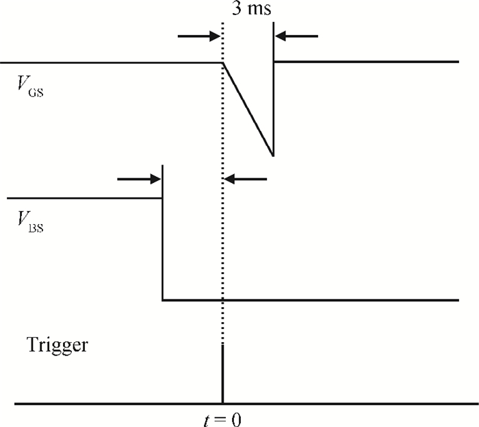
Fig. 1.
Timing diagrams for gate and substrate pulsing and triggering[12].
SEMICONDUCTOR DEVICES
Ahmed Chaouki Megherbi1, , Said Benramache2, and Abderrazak Guettaf1
Corresponding author: Ahmed Chaouki, Email:megherbic@yahoo.fr; Megherbi, benramache.said@gmail.com
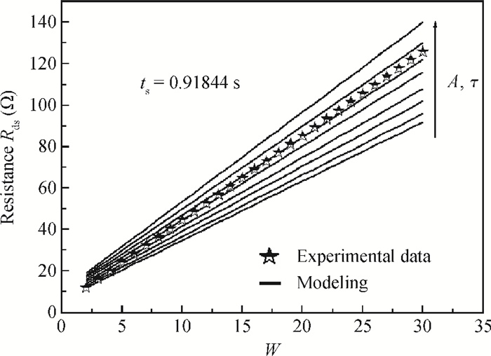
Abstract: This study focuses on modeling the effects of deep hole traps, mainly the effect of the substrate (backgating effect) in a GaAs transistor MESFT. This effect is explained by the existence, at the interface, of a space charge zone. Any modulation in this area leads to response levels trapping the holes therein to the operating temperature. We subsequently developed a model treating the channel substrate interface as an N-P junction, allowing us to deduce the time dependence of the component parameters of the total resistance Rds, the pinch-off voltage VP, channel resistance, fully open Rco and the parasitic series resistance RS to bind the effect trap holes H1 and H0. When compared with the experimental results, the values of the RDS (tS) model for both traps show that there is an agreement between theory and experiment; it has inferred parameter traps, namely the density and the time constant of the trap. This means that a space charge region exists at the channel-substrate interface and that the properties can be approximated to an N-P junction.
Key words: traps, pinch-off voltage, resistance, channel substrate interface
| [1] |
Akinlami J O, Ashamu A O. Optical properties of GaAs. Journal of Semiconductors, 2013, 34(3):032002 doi: 10.1088/1674-4926/34/3/032002
|
| [2] |
Zhang Ying, Wang Zhigong, Xu Jian, et al. Design of a low noise distributed amplifier with adjustable gain control in 0.15μm GaAs PHEMT. Journal of Semiconductors, 2013, 33(3):035003 http://www.jos.ac.cn/bdtxbcn/ch/reader/view_abstract.aspx?file_no=11071901&flag=1
|
| [3] |
Parida R K, Agrawala N C, Dash G N, et al. Characteristics of a GaN-based Gunn diode for THz signal generation. Journal of Semiconductors, 2013, 33(8):084001 http://www.jos.ac.cn/bdtxbcn/ch/reader/view_abstract.aspx?file_no=12012101&flag=1
|
| [4] |
Ma Xiangrong, Shi Wei, Ji WWeili, et al. Light controlled prebreakdown characteristics of a semi-insulating GaAs photoconductive switch. Journal of Semiconductors, 2013, 32(12):124006 http://www.jos.ac.cn/bdtxbcn/ch/reader/view_abstract.aspx?file_no=11042002&flag=1
|
| [5] |
Lü Siyu, Qu Xiaosheng. AlGaAs/GaAs tunnel junctions in a 4-J tandem solar cell. Journal of Semiconductors, 2011, 32(11):112003 doi: 10.1088/1674-4926/32/11/112003
|
| [6] |
Kunihiro K, Ohno Y. Design consideration for buried p layers to suppress substrate-trapping effects in GaAs MESFETs. Solid-State Electron, 2001, 45(8):1763 http://adsabs.harvard.edu/abs/2001SSEle..45.1763K
|
| [7] |
Markov A V, Biberin V I, Polyakov A Y, et al. Synthesis solute diffusion growth of bulk GaAs:effects of growth temperature and stoichiometry. Solid-State Electron, 2007, 51(5):1039 http://cat.inist.fr/?aModele=afficheN&cpsidt=18953028
|
| [8] |
Wakejima A, Ota K, Matsunaga K. Study of surface-trap-induced gate depletion region of field-modulating plate GaAs-FETs. Solid-State Electron, 2006, 50(2):372 http://www.sciencedirect.com/science/article/pii/S0038110106000141?via%3Dihub
|
| [9] |
Qi H, Wang Q, Zhang X, et al. Theoretical and experimental study of laser induced damage on GaAs by nanosecond pulsed irradiation. Opt Lasers Eng, 2011, 49(2):285 doi: 10.1016/j.optlaseng.2010.10.004
|
| [10] |
Kajara T T, Gaeta A L. Q switching of a diode-pumped Nd:YAG laser with GaAs. Opt Lett, 1996, 21(16):1244 doi: 10.1364/OL.21.001244
|
| [11] |
Parida R K, Agrawala N C, Dash G N, et al. Characteristics of a GaN-based Gunn diode for THz signal generation. Journal of Semiconductors, 2012, 33(8):084001 doi: 10.1088/1674-4926/33/8/084001
|
| [12] |
Sengouga N, Jones B K. Backgating effects in GaAs FETs with a channel-semi-insulating substrate boundary. Solid-State Electron, 1995, 38(7):1413 doi: 10.1016/0038-1101(94)00249-F
|
| [13] |
Sengouga N, Abdeslam N A. Dependence of backgating on the type of deep centres in the substrate of GaAs FETs. Solid-State Electron, 2008, 52(5):1039 http://dspace.univ-biskra.dz:8080/jspui/bitstream/123456789/2717/1/Dependence%20of%20backgating%20on%20the%20type%20of%20deep%20centres%20in%20the%20substrate%20of%20GaAs%20FETs2.pdf
|
| [14] |
Dehimi L, Sengouga N, Jones B K. Modelling of semiconductor diodes made of high defect concentration, irradiated, high resistivity and semi-insulating material:the current-voltage characteristics. Nuclear Instruments and Methods in Physics Research A, 2004, 519(3):532 doi: 10.1016/j.nima.2003.10.088
|
| [15] |
Kunihiro K, Ohno Y. design considerations for buried p-layers to suppress substrate-trapping effects in GaAs MESFETs. Solid-State Electron, 2001, 45(8):1763 http://adsabs.harvard.edu/abs/2001SSEle..45.1763K
|
| [16] |
Khuchua N P, Khvedelidze L V, Gorev N B, et al. determination of deep trap concentration at channel-substrate interface in GaAs MESFET using sidegating measurements. Solid-State Electron, 2002, 46(7):1463 http://adsabs.harvard.edu/abs/2002SSEle..46.1463K
|
| [17] |
Jin G, Jones B K. Characterisation of the time-dependent properties of GaAs FETs. Semicond Sci Technol, 1990, 5(2):395 doi: 10.1088/0268-1242/5/5/004
|
| [18] |
Fukui H. Optimal noise figure of microwave GaAs MESFETs. IEEE Trans Electron Devices, 1979, ED-26(7):1032 http://ieeexplore.ieee.org/document/1480119/
|


Article views: 2830 Times PDF downloads: 10 Times Cited by: 0 Times
Received: 20 September 2013 Revised: 27 October 2013 Online: Published: 01 March 2014
| Citation: |
Ahmed Chaouki Megherbi, Said Benramache, Abderrazak Guettaf. Backgating effect in GaAs FETs with a channel-semi-insulating substrate boundary[J]. Journal of Semiconductors, 2014, 35(3): 034004. doi: 10.1088/1674-4926/35/3/034004
A C Megherbi, S Benramache, A Guettaf. Backgating effect in GaAs FETs with a channel-semi-insulating substrate boundary[J]. J. Semicond., 2014, 35(3): 034004. doi: 10.1088/1674-4926/35/3/034004.
Export: BibTex EndNote

|
| [1] |
Akinlami J O, Ashamu A O. Optical properties of GaAs. Journal of Semiconductors, 2013, 34(3):032002 doi: 10.1088/1674-4926/34/3/032002
|
| [2] |
Zhang Ying, Wang Zhigong, Xu Jian, et al. Design of a low noise distributed amplifier with adjustable gain control in 0.15μm GaAs PHEMT. Journal of Semiconductors, 2013, 33(3):035003 http://www.jos.ac.cn/bdtxbcn/ch/reader/view_abstract.aspx?file_no=11071901&flag=1
|
| [3] |
Parida R K, Agrawala N C, Dash G N, et al. Characteristics of a GaN-based Gunn diode for THz signal generation. Journal of Semiconductors, 2013, 33(8):084001 http://www.jos.ac.cn/bdtxbcn/ch/reader/view_abstract.aspx?file_no=12012101&flag=1
|
| [4] |
Ma Xiangrong, Shi Wei, Ji WWeili, et al. Light controlled prebreakdown characteristics of a semi-insulating GaAs photoconductive switch. Journal of Semiconductors, 2013, 32(12):124006 http://www.jos.ac.cn/bdtxbcn/ch/reader/view_abstract.aspx?file_no=11042002&flag=1
|
| [5] |
Lü Siyu, Qu Xiaosheng. AlGaAs/GaAs tunnel junctions in a 4-J tandem solar cell. Journal of Semiconductors, 2011, 32(11):112003 doi: 10.1088/1674-4926/32/11/112003
|
| [6] |
Kunihiro K, Ohno Y. Design consideration for buried p layers to suppress substrate-trapping effects in GaAs MESFETs. Solid-State Electron, 2001, 45(8):1763 http://adsabs.harvard.edu/abs/2001SSEle..45.1763K
|
| [7] |
Markov A V, Biberin V I, Polyakov A Y, et al. Synthesis solute diffusion growth of bulk GaAs:effects of growth temperature and stoichiometry. Solid-State Electron, 2007, 51(5):1039 http://cat.inist.fr/?aModele=afficheN&cpsidt=18953028
|
| [8] |
Wakejima A, Ota K, Matsunaga K. Study of surface-trap-induced gate depletion region of field-modulating plate GaAs-FETs. Solid-State Electron, 2006, 50(2):372 http://www.sciencedirect.com/science/article/pii/S0038110106000141?via%3Dihub
|
| [9] |
Qi H, Wang Q, Zhang X, et al. Theoretical and experimental study of laser induced damage on GaAs by nanosecond pulsed irradiation. Opt Lasers Eng, 2011, 49(2):285 doi: 10.1016/j.optlaseng.2010.10.004
|
| [10] |
Kajara T T, Gaeta A L. Q switching of a diode-pumped Nd:YAG laser with GaAs. Opt Lett, 1996, 21(16):1244 doi: 10.1364/OL.21.001244
|
| [11] |
Parida R K, Agrawala N C, Dash G N, et al. Characteristics of a GaN-based Gunn diode for THz signal generation. Journal of Semiconductors, 2012, 33(8):084001 doi: 10.1088/1674-4926/33/8/084001
|
| [12] |
Sengouga N, Jones B K. Backgating effects in GaAs FETs with a channel-semi-insulating substrate boundary. Solid-State Electron, 1995, 38(7):1413 doi: 10.1016/0038-1101(94)00249-F
|
| [13] |
Sengouga N, Abdeslam N A. Dependence of backgating on the type of deep centres in the substrate of GaAs FETs. Solid-State Electron, 2008, 52(5):1039 http://dspace.univ-biskra.dz:8080/jspui/bitstream/123456789/2717/1/Dependence%20of%20backgating%20on%20the%20type%20of%20deep%20centres%20in%20the%20substrate%20of%20GaAs%20FETs2.pdf
|
| [14] |
Dehimi L, Sengouga N, Jones B K. Modelling of semiconductor diodes made of high defect concentration, irradiated, high resistivity and semi-insulating material:the current-voltage characteristics. Nuclear Instruments and Methods in Physics Research A, 2004, 519(3):532 doi: 10.1016/j.nima.2003.10.088
|
| [15] |
Kunihiro K, Ohno Y. design considerations for buried p-layers to suppress substrate-trapping effects in GaAs MESFETs. Solid-State Electron, 2001, 45(8):1763 http://adsabs.harvard.edu/abs/2001SSEle..45.1763K
|
| [16] |
Khuchua N P, Khvedelidze L V, Gorev N B, et al. determination of deep trap concentration at channel-substrate interface in GaAs MESFET using sidegating measurements. Solid-State Electron, 2002, 46(7):1463 http://adsabs.harvard.edu/abs/2002SSEle..46.1463K
|
| [17] |
Jin G, Jones B K. Characterisation of the time-dependent properties of GaAs FETs. Semicond Sci Technol, 1990, 5(2):395 doi: 10.1088/0268-1242/5/5/004
|
| [18] |
Fukui H. Optimal noise figure of microwave GaAs MESFETs. IEEE Trans Electron Devices, 1979, ED-26(7):1032 http://ieeexplore.ieee.org/document/1480119/
|

 WeChat ID
Journal of Semiconductors © 2017 All Rights Reserved 京ICP备05085259号-2

 DownLoad:

