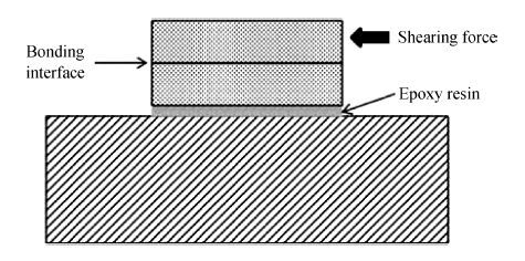
Fig. 1.
Direct wafer bonding with a SiO$_{2}$ layer at the interface.
SEMICONDUCTOR TECHNOLOGY
Xiaoqing Wang, Yude Yu and Jin Ning
Corresponding author: Corresponding author. Email: yudeyu@semi.ac.cn
Abstract: A silicon wafer direct bonding with a thin SiO2 layer at the interface was investigated. An atomic force microscope (AFM) was employed to characterize the surface roughness and a shearing test was carried out to evaluate the bonding strength. Experiments were performed to analyze the relations of surface roughness and bonding strength with the thickness of SiO2 which was grown by thermal oxidation and plasma enhanced chemical vapor deposition (PECVD) respectively. The bonding strength can reach up to 18 MPa for thermal oxidation and 8 MPa for PECVD after a 2-h 400 ℃ annealing. Results indicate that the bonding strength is negatively correlated to the thickness of SiO2 at the interface, which is important in designing the MEMS-based devices and other devices built with wafer direct bonding.
Key words: wafer direct bonding, surface roughness, bonding strength
| [1] | |
| [2] | |
| [3] | |
| [4] | |
| [5] | |
| [6] | |
| [7] | |
| [8] | |
| [9] | |
| [10] | |
| [11] | |
| [12] | |
| [13] | |
| [14] |
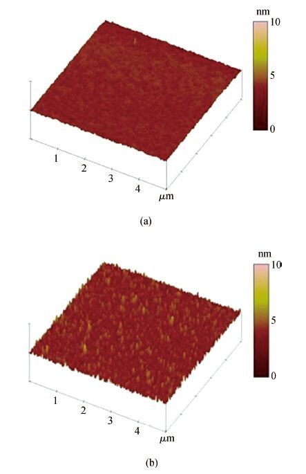

Table 1. Bonding strength as a function of the SiO$_{2}$ thickness by PECVD and thermal oxidation.
 DownLoad: CSV
| [1] | |
| [2] | |
| [3] | |
| [4] | |
| [5] | |
| [6] | |
| [7] | |
| [8] | |
| [9] | |
| [10] | |
| [11] | |
| [12] | |
| [13] | |
| [14] |


Article views: 3442 Times PDF downloads: 70 Times Cited by: 0 Times
Received: 13 August 2015 Revised: Online: Published: 01 May 2016
| Citation: |
Xiaoqing Wang, Yude Yu, Jin Ning. Researching the silicon direct wafer bonding with interfacial SiO2 layer[J]. Journal of Semiconductors, 2016, 37(5): 056001. doi: 10.1088/1674-4926/37/5/056001
X Q Wang, Y D Yu, J Ning. Researching the silicon direct wafer bonding with interfacial SiO2 layer[J]. J. Semicond., 2016, 37(5): 056001. doi: 10.1088/1674-4926/37/5/056001.
Export: BibTex EndNote

|
| [1] | |
| [2] | |
| [3] | |
| [4] | |
| [5] | |
| [6] | |
| [7] | |
| [8] | |
| [9] | |
| [10] | |
| [11] | |
| [12] | |
| [13] | |
| [14] |

 WeChat ID
Journal of Semiconductors © 2017 All Rights Reserved 京ICP备05085259号-2