


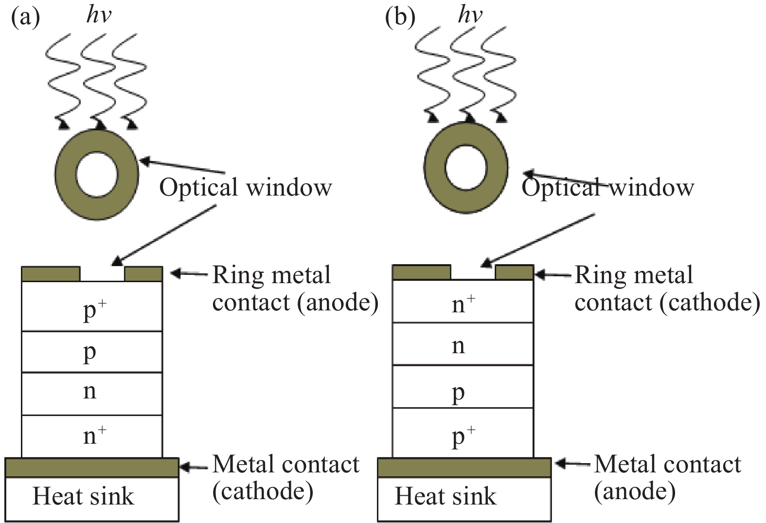
Fig. 1.
(Color online) (a) Top mounted (TM) and (b) flip-chip (FC) DDR IMPATT structures under optical illumination.
SEMICONDUCTOR DEVICES
Atanu Banerjee1, and M. Mitra2
Corresponding author: Atanu Banerjee, E-mail: atanur_mailbox@yahoo.com, monojit_m1@yahoo.co.in
Abstract: A reverse biased p–n junction diode with proper resonant cavity and boundary conditions is able to generate rf power and shows normal DC and small signal properties designed with semiconductor materials like 4H-SiC, GaAs, InP, Si-based DDR IMPATT structure at Ka band with dark condition. But when it is exposed to optical illumination through a proper optical window for both top mounted (TM) and flip chip (FC) configuration, it shows the influence on the oscillator performances in that band of frequency. The simulated results are analyzed for 36 GHz window frequency in each of the diodes and relative differences are found in power output and frequency of all these diodes with variable intensities of illumination. Finally it is found that optical control has immense effect in both FC and TM mode regarding the reduction of output power and shifting of operating frequency from which optimization is done for the best optically sensitive material for IMPATT diode.
Key words: optical modulation, flip chip structure, top mounted structure, window frequency, DDR IMPATT diode
| [1] |
Karmakara P K, Maiti M, Mondala S, et al. Determination of window frequency in the millimeter wave band in the range of 58° north through 45° south over the globe. Adv Space Res, 2011, 48: 146 doi: 10.1016/j.asr.2011.02.019
|
| [2] |
Chang Y, Hellum J M, Paul J A, et al. Millimeter-wave IMPATT sources for Communication Applications. IEEE MTT-S International Microwave Symposium Digest, 1977: 216
|
| [3] |
Gray W W, Kikushima L, Morentc N P, et al. Applying IMPATT power sources to modern microwave system. IEEE J Solid-State Circuits, 1969, 4(6): 409 doi: 10.1109/JSSC.1969.1050046
|
| [4] |
Vyas H P, Gutmann R J, Borrego J M, et al. Effect of hole versus electron photocurrent on microwave-optical interactions in impatt oscillators. IEEE Trans Electron Devices, 1979, 26(3): 232 doi: 10.1109/T-ED.1979.19411
|
| [5] |
Acharyya A, Banerjee S, Banerjee J P, et al. Optical control of millimeter-wave lateral double-drift region silicon IMPATT device. Radioengineering, 2012, 21(4): 1208
|
| [6] |
Mukherjee M, Majumder N, Roy S K, et al. Prospects of 4H-SiC double drift region IMPATT device as a photo-sensitive high-power source at 0.7 terahertz frequency regime. Active and Passive Electronic Components, 2008: 1
|
| [7] |
Acharyya A, Banerjee J P. A comparative study on the effect of optical illumination on Si1−xGex and Si Based DDR IMPATT diodes at W-band. Iran J Electr Electron Eng, 2011, 7(3): 179
|
| [8] |
Yen H W, Barnoski M K, Hunsperger R G, et al. Switching of GaAs IMPATT diode oscillator by optical illumination. Appl Phys Lett, 1977, 31: 120 doi: 10.1063/1.89581
|
| [9] |
Mukherjee R, Banerjee J P. Effect of electron and hole dominant photocurrent on the millimeter-wave properties of Indium Phosphide Impatt diode at 94 GHz. Semicond Sci Technol, 1994, 9: 1 doi: 10.1088/0268-1242/9/1/001
|
| [10] |
Mukherjee M, Majumdar N. Optically illuminated 4H-SiC terahertz IMPATT device. Egypt J Solids, 2007, 30(1): 87
|
| [11] |
Acharyya A, Banerjee J P. Dependence of avalanche response time on photon flux incident on DDR silicon IMPATT devices. The 32nd PIERS, Moscow (Russia), 2012: 1
|
| [12] |
Roy S K, Banerjee J P, Pati S P, et al. A Computer analysis of the distribution of high frequency negative resistance in the depletion layer of IMPATT diodes. Proc 4th Conf On Num Anal of Semiconductor Devices (NASECODE IV) (Dublin) (Dublin: Boole), 1985: 494
|
| [13] |
Banerjee A, Mitra M. Analysis of Ka band DDR IMPATT diode based on different solidstate Materials. IJSCE, 2013, 3(2): 6
|
| [14] |
Roy S K, Sridharan M, Gosh R, et al. Computer methods for the dc field and carrier current profiles in impatt devices starting from the field extremum in the depletion layer. Proc of NASECODE-I Conf. on Numerical Analysis of Semiconductor Devices. Dublin: Boole Press, 1979: 266
|
| [15] |
Mazumder N, Roy S K. Effect of Enhanced Leakage Current on the Microwave Negative Resistance of High Efficiency GaAs Double Drift Region IMPATT Diode. IETE J Res, 1994, 40(1): 31 doi: 10.1080/03772063.1994.11437161
|
| [16] |
Mazumder N, Roy S K. Saturation current induced effects on the microwave and millimetre wave performance of GaAs double drift region IMPATTs. Int J Electron, 1991, 71(2): 227 doi: 10.1080/00207219108925471
|
| [17] |
Gummel H K, Blue J L. A small-signal theory of avalanche noise in IMPATT diodes. IEEE Trans Electron Devices, 1967, 14(9): 569 doi: 10.1109/T-ED.1967.16005
|
| [18] |
Vyas H P, Gutmann R J, Borrego J M, et al. Leakage current enhancement in IMPATT oscillators by photoexcitation. Electron Lett, 1977, 13(7): 189 doi: 10.1049/el:19770139
|
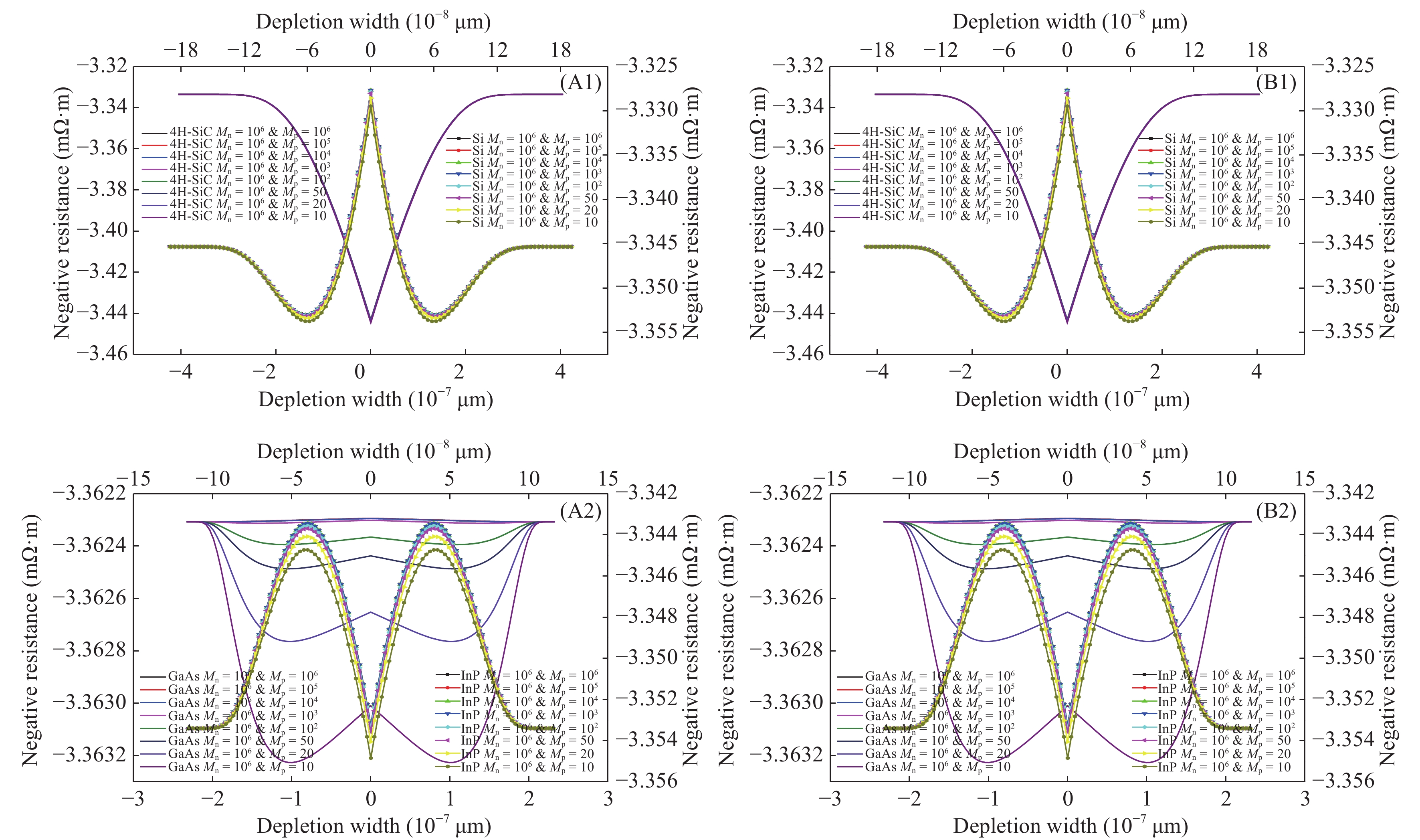
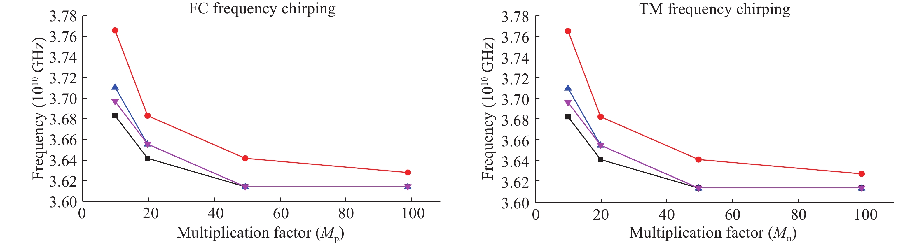
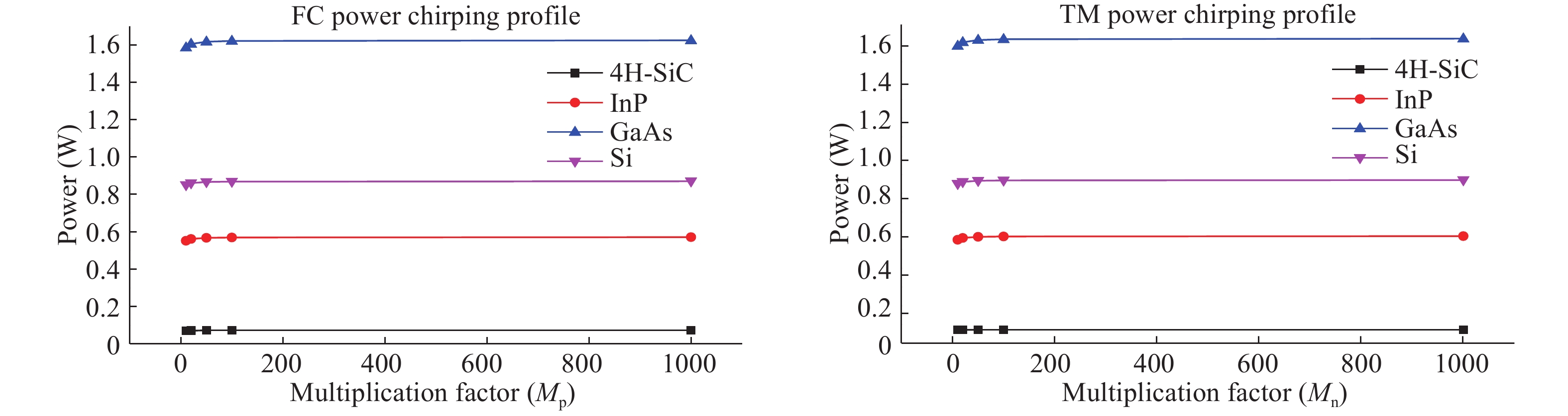
Table 1. All material parameters are at 300 K.
| Material | Em (V/m) | J0 (A/m2) | Eg (eV) | WDP (μm) | NA (m−3) | ND (m−3) | VB (V) | VA (V) |
| 4H-SiC | 5.39 × 10 8 | 3.4 × 10 10 | 3.20 | 0.808 | 1.09 × 10 23 | 8.47 × 10 23 | 1.16 | 0.13 |
| GaAs | 1.61 × 10 8 | 4.12 × 10 10 | 1.44 | 0.0464 | 1.0 × 10 24 | 5.84 × 10 24 | 1.32 | 0.17 |
| InP | 7.7 × 10 7 | 2.54 × 10 10 | 1.34 | 0.23 | 1.6 × 10 23 | 6.18 × 10 23 | 1.75 | 0.17 |
| Si | 4.2 × 10 7 | 7.12 × 10 9 | 1.12 | 0.38 | 1.0 × 10 23 | 2.19 × 10 23 | 2.77 | 0.28 |
 DownLoad: CSV
Table 2. Parameters at dark condition: Mn = 106 & Mp = 106.
| Material | Fop (GHz) | Gop (s/m2) | Bop (s/m2) | PRF (W) | Qop | ZRop (Ωm2) | ZXop (Ωm2) | η (%) |
| 4H-SiC | 36 | −2.7 × 10 8 | 2.614 × 10 8 | 0.072 | 0.977 | −1.92 × 10 −9 | 1.87 × 10 −9 | 11.547 |
| GaAs | 36 | −4.7 × 10 9 | 4.55 × 10 9 | 1.63 | 0.975 | −1.11 × 10 −10 | 1.07 × 10 −10 | 11.357 |
| InP | 36 | −9.4 × 10 8 | 9.22 × 10 8 | 0.572 | 0.983 | −5.42 × 10 −10 | 5.33 × 10 −10 | 11.767 |
| Si | 36 | −5.67 × 10 8 | 5.58 × 10 8 | 0.871 | 0.984 | −8.96 × 10 −10 | 8.82 × 10 −10 | 11.685 |
DownLoad: CSV
Table 3. Parameters for flip-chip orientation.
| Material | Mn | Mp | FDesign (GHz) | FChirp (GHz) | PDesign(W) | PChirp(W) |
| 4H-SiC | 106 | 100 | 36 | 36.14 | 0.071 64 | 0.071 51 |
| 50 | 36 | 36.14 | 0.071 64 | 0.071 39 | ||
| 20 | 36 | 36.42 | 0.071 64 | 0.071 03 | ||
| 10 | 36 | 36.83 | 0.071 64 | 0.070 43 | ||
| GaAs | 106 | 100 | 36 | 36.14 | 1.625 | 1.6213 |
| 50 | 36 | 36.14 | 1.625 | 1.6172 | ||
| 20 | 36 | 36.56 | 1.625 | 1.6052 | ||
| 10 | 36 | 37.11 | 1.625 | 1.5856 | ||
| InP | 106 | 100 | 36 | 36.14 | 0.5715 | 0.5695 |
| 50 | 36 | 36.14 | 0.5715 | 0.5675 | ||
| 20 | 36 | 36.28 | 0.5715 | 0.5614 | ||
| 10 | 36 | 36.56 | 0.5715 | 0.5517 | ||
| Si | 106 | 100 | 36 | 36.14 | 0.870 36 | 0.8683 |
| 50 | 36 | 36.14 | 0.870 36 | 0.8663 | ||
| 20 | 36 | 36.56 | 0.870 36 | 0.8602 | ||
| 10 | 36 | 36.97 | 0.870 36 | 0.8504 |
DownLoad: CSV
Table 4. Parameters for top mounted orientation.
| Material | Mn | Mp | FDesign (GHz) | FChirp (GHz) | PDesign(W) | PChirp (W) |
| 4H-SiC | 100 | 106 | 36 | 36.14 | 0.071 64 | 0.071 51 |
| 50 | 36 | 36.14 | 0.071 64 | 0.071 39 | ||
| 20 | 36 | 36.42 | 0.071 64 | 0.071 03 | ||
| 10 | 36 | 36.83 | 0.071 64 | 0.070 43 | ||
| GaAs | 100 | 106 | 36 | 36.14 | 1.625 | 1.6213 |
| 50 | 36 | 36.14 | 1.625 | 1.6172 | ||
| 20 | 36 | 36.56 | 1.625 | 1.6052 | ||
| 10 | 36 | 37.11 | 1.625 | 1.5856 | ||
| InP | 100 | 106 | 36 | 36.28 | 0.5715 | 0.5695 |
| 50 | 36 | 36.42 | 0.5715 | 0.5675 | ||
| 20 | 36 | 36.83 | 0.5715 | 0.5614 | ||
| 10 | 36 | 37.66 | 0.5715 | 0.5517 | ||
| Si | 100 | 106 | 36 | 36.14 | 0.870 36 | 0.8683 |
| 50 | 36 | 36.14 | 0.870 36 | 0.8663 | ||
| 20 | 36 | 36.56 | 0.870 36 | 0.8602 | ||
| 10 | 36 | 36.97 | 0.870 36 | 0.8504 |
DownLoad: CSV
| [1] |
Karmakara P K, Maiti M, Mondala S, et al. Determination of window frequency in the millimeter wave band in the range of 58° north through 45° south over the globe. Adv Space Res, 2011, 48: 146 doi: 10.1016/j.asr.2011.02.019
|
| [2] |
Chang Y, Hellum J M, Paul J A, et al. Millimeter-wave IMPATT sources for Communication Applications. IEEE MTT-S International Microwave Symposium Digest, 1977: 216
|
| [3] |
Gray W W, Kikushima L, Morentc N P, et al. Applying IMPATT power sources to modern microwave system. IEEE J Solid-State Circuits, 1969, 4(6): 409 doi: 10.1109/JSSC.1969.1050046
|
| [4] |
Vyas H P, Gutmann R J, Borrego J M, et al. Effect of hole versus electron photocurrent on microwave-optical interactions in impatt oscillators. IEEE Trans Electron Devices, 1979, 26(3): 232 doi: 10.1109/T-ED.1979.19411
|
| [5] |
Acharyya A, Banerjee S, Banerjee J P, et al. Optical control of millimeter-wave lateral double-drift region silicon IMPATT device. Radioengineering, 2012, 21(4): 1208
|
| [6] |
Mukherjee M, Majumder N, Roy S K, et al. Prospects of 4H-SiC double drift region IMPATT device as a photo-sensitive high-power source at 0.7 terahertz frequency regime. Active and Passive Electronic Components, 2008: 1
|
| [7] |
Acharyya A, Banerjee J P. A comparative study on the effect of optical illumination on Si1−xGex and Si Based DDR IMPATT diodes at W-band. Iran J Electr Electron Eng, 2011, 7(3): 179
|
| [8] |
Yen H W, Barnoski M K, Hunsperger R G, et al. Switching of GaAs IMPATT diode oscillator by optical illumination. Appl Phys Lett, 1977, 31: 120 doi: 10.1063/1.89581
|
| [9] |
Mukherjee R, Banerjee J P. Effect of electron and hole dominant photocurrent on the millimeter-wave properties of Indium Phosphide Impatt diode at 94 GHz. Semicond Sci Technol, 1994, 9: 1 doi: 10.1088/0268-1242/9/1/001
|
| [10] |
Mukherjee M, Majumdar N. Optically illuminated 4H-SiC terahertz IMPATT device. Egypt J Solids, 2007, 30(1): 87
|
| [11] |
Acharyya A, Banerjee J P. Dependence of avalanche response time on photon flux incident on DDR silicon IMPATT devices. The 32nd PIERS, Moscow (Russia), 2012: 1
|
| [12] |
Roy S K, Banerjee J P, Pati S P, et al. A Computer analysis of the distribution of high frequency negative resistance in the depletion layer of IMPATT diodes. Proc 4th Conf On Num Anal of Semiconductor Devices (NASECODE IV) (Dublin) (Dublin: Boole), 1985: 494
|
| [13] |
Banerjee A, Mitra M. Analysis of Ka band DDR IMPATT diode based on different solidstate Materials. IJSCE, 2013, 3(2): 6
|
| [14] |
Roy S K, Sridharan M, Gosh R, et al. Computer methods for the dc field and carrier current profiles in impatt devices starting from the field extremum in the depletion layer. Proc of NASECODE-I Conf. on Numerical Analysis of Semiconductor Devices. Dublin: Boole Press, 1979: 266
|
| [15] |
Mazumder N, Roy S K. Effect of Enhanced Leakage Current on the Microwave Negative Resistance of High Efficiency GaAs Double Drift Region IMPATT Diode. IETE J Res, 1994, 40(1): 31 doi: 10.1080/03772063.1994.11437161
|
| [16] |
Mazumder N, Roy S K. Saturation current induced effects on the microwave and millimetre wave performance of GaAs double drift region IMPATTs. Int J Electron, 1991, 71(2): 227 doi: 10.1080/00207219108925471
|
| [17] |
Gummel H K, Blue J L. A small-signal theory of avalanche noise in IMPATT diodes. IEEE Trans Electron Devices, 1967, 14(9): 569 doi: 10.1109/T-ED.1967.16005
|
| [18] |
Vyas H P, Gutmann R J, Borrego J M, et al. Leakage current enhancement in IMPATT oscillators by photoexcitation. Electron Lett, 1977, 13(7): 189 doi: 10.1049/el:19770139
|


Article views: 3149 Times PDF downloads: 26 Times Cited by: 0 Times
Received: 14 March 2017 Revised: 09 May 2017 Online: Uncorrected proof: 30 October 2017Accepted Manuscript: 13 November 2017Published: 01 November 2017
| Citation: |
Atanu Banerjee, M. Mitra. Effect of optical illumination on DDR IMPATT diode at 36 GHz[J]. Journal of Semiconductors, 2017, 38(11): 114002. doi: 10.1088/1674-4926/38/11/114002
****
A Banerjee, M. Mitra. Effect of optical illumination on DDR IMPATT diode at 36 GHz[J]. J. Semicond., 2017, 38(11): 114002. doi: 10.1088/1674-4926/38/11/114002.

|
| [1] |
Karmakara P K, Maiti M, Mondala S, et al. Determination of window frequency in the millimeter wave band in the range of 58° north through 45° south over the globe. Adv Space Res, 2011, 48: 146 doi: 10.1016/j.asr.2011.02.019
|
| [2] |
Chang Y, Hellum J M, Paul J A, et al. Millimeter-wave IMPATT sources for Communication Applications. IEEE MTT-S International Microwave Symposium Digest, 1977: 216
|
| [3] |
Gray W W, Kikushima L, Morentc N P, et al. Applying IMPATT power sources to modern microwave system. IEEE J Solid-State Circuits, 1969, 4(6): 409 doi: 10.1109/JSSC.1969.1050046
|
| [4] |
Vyas H P, Gutmann R J, Borrego J M, et al. Effect of hole versus electron photocurrent on microwave-optical interactions in impatt oscillators. IEEE Trans Electron Devices, 1979, 26(3): 232 doi: 10.1109/T-ED.1979.19411
|
| [5] |
Acharyya A, Banerjee S, Banerjee J P, et al. Optical control of millimeter-wave lateral double-drift region silicon IMPATT device. Radioengineering, 2012, 21(4): 1208
|
| [6] |
Mukherjee M, Majumder N, Roy S K, et al. Prospects of 4H-SiC double drift region IMPATT device as a photo-sensitive high-power source at 0.7 terahertz frequency regime. Active and Passive Electronic Components, 2008: 1
|
| [7] |
Acharyya A, Banerjee J P. A comparative study on the effect of optical illumination on Si1−xGex and Si Based DDR IMPATT diodes at W-band. Iran J Electr Electron Eng, 2011, 7(3): 179
|
| [8] |
Yen H W, Barnoski M K, Hunsperger R G, et al. Switching of GaAs IMPATT diode oscillator by optical illumination. Appl Phys Lett, 1977, 31: 120 doi: 10.1063/1.89581
|
| [9] |
Mukherjee R, Banerjee J P. Effect of electron and hole dominant photocurrent on the millimeter-wave properties of Indium Phosphide Impatt diode at 94 GHz. Semicond Sci Technol, 1994, 9: 1 doi: 10.1088/0268-1242/9/1/001
|
| [10] |
Mukherjee M, Majumdar N. Optically illuminated 4H-SiC terahertz IMPATT device. Egypt J Solids, 2007, 30(1): 87
|
| [11] |
Acharyya A, Banerjee J P. Dependence of avalanche response time on photon flux incident on DDR silicon IMPATT devices. The 32nd PIERS, Moscow (Russia), 2012: 1
|
| [12] |
Roy S K, Banerjee J P, Pati S P, et al. A Computer analysis of the distribution of high frequency negative resistance in the depletion layer of IMPATT diodes. Proc 4th Conf On Num Anal of Semiconductor Devices (NASECODE IV) (Dublin) (Dublin: Boole), 1985: 494
|
| [13] |
Banerjee A, Mitra M. Analysis of Ka band DDR IMPATT diode based on different solidstate Materials. IJSCE, 2013, 3(2): 6
|
| [14] |
Roy S K, Sridharan M, Gosh R, et al. Computer methods for the dc field and carrier current profiles in impatt devices starting from the field extremum in the depletion layer. Proc of NASECODE-I Conf. on Numerical Analysis of Semiconductor Devices. Dublin: Boole Press, 1979: 266
|
| [15] |
Mazumder N, Roy S K. Effect of Enhanced Leakage Current on the Microwave Negative Resistance of High Efficiency GaAs Double Drift Region IMPATT Diode. IETE J Res, 1994, 40(1): 31 doi: 10.1080/03772063.1994.11437161
|
| [16] |
Mazumder N, Roy S K. Saturation current induced effects on the microwave and millimetre wave performance of GaAs double drift region IMPATTs. Int J Electron, 1991, 71(2): 227 doi: 10.1080/00207219108925471
|
| [17] |
Gummel H K, Blue J L. A small-signal theory of avalanche noise in IMPATT diodes. IEEE Trans Electron Devices, 1967, 14(9): 569 doi: 10.1109/T-ED.1967.16005
|
| [18] |
Vyas H P, Gutmann R J, Borrego J M, et al. Leakage current enhancement in IMPATT oscillators by photoexcitation. Electron Lett, 1977, 13(7): 189 doi: 10.1049/el:19770139
|

 WeChat ID
Journal of Semiconductors © 2017 All Rights Reserved 京ICP备05085259号-2


