


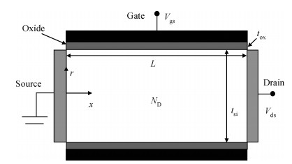
Fig. 1.
Cross-sectional view of the investigated JLGAA MOSFET, and the coordinate System.
SEMICONDUCTOR DEVICES
T. Bendib, F. Djeffal and M. Meguellati
Corresponding author: F. Djeffal, Email:faycal.djeffal@univ-batna.dz, faycaldzdz@hotmail.com
Abstract: An analytical investigation has been proposed to study the subthreshold behavior of junctionless gates all around (JLGAA) MOSFET for nanoscale CMOS analog applications. Based on 2-D analytical analysis, a new subthreshold swing model for short-channel JLGAA MOSFETs is developed. The analysis has been used to calculate the subthreshold swing and to compare the performance of the investigated design and conventional GAA MOSFET, where the comparison of device architectures shows that the JLGAA MOSFET exhibits a superior performance with respect to the conventional inversion-mode GAA MOSFET in terms of the fabrication process and electrical behavior in the subthreshold domain. The analytical models have been validated by 2-D numerical simulations. The proposed analytical models are used to formulate the objectives functions. The overall objective function is formulated by means of a weighted sum approach to search the optimal electrical and dimensional device parameters in order to obtain the better scaling capability and the electrical performance of the device for ultra-low power applications.
Key words: junctionless, optimization, subthreshold, nanoscale, multiobjective
| [1] |
Djeffal F, Goughali Z, Dibi Z, et al. Analytical analysis of nanoscale multiple gate MOSFETs including effects of hot-carrier induced interface charges. Microelectron Reliab, 2009, 49: 377 doi: 10.1016/j.microrel.2008.12.011
|
| [2] |
Tsompatzoglou A, Dimitriadis C A, Clerc R, et al. Semi-analytical modeling of short-channel effects in Si and Ge symmetrical double-gate MOSFETs. IEEE Trans Electron Devices, 2007, 54: 1943 doi: 10.1109/TED.2007.901075
|
| [3] |
Meguellati M, Djeffal F. New dual-dielectric gate all around (DDGAA) RADFET dosimeter design to improve the radiation sensitivity. Nuclear Instruments and Methods in Physics Research Section A, 2012, 683: 24 doi: 10.1016/j.nima.2012.04.072
|
| [4] |
Bendib T, Djeffal F. Electrical performance optimization of nanoscale double-gate MOSFETs using multi-objective genetic algorithms. IEEE Trans Electron Devices, 2011, 58: 3743 doi: 10.1109/TED.2011.2163820
|
| [5] |
International Technology Roadmap for Semiconductors (ITRS). [Online]. Available: http://public.itrs.net T K Chiang. A new quasi-2-D threshold voltage model for short-channel junctionless cylindrical surrounding gate (JLCSG) MOSFETs. IEEE Trans Electron Devices, 2012, 59: 3127
|
| [6] |
Lee C W, Afzalian A, Akhavan N D, et al. Junctionless multigate field-effect transistor. Appl Phys Lett, 2009, 94: 053511 doi: 10.1063/1.3079411
|
| [7] |
Lee C W, Borne A, Ferain I, et al. High-temperature performance of silicon junctionless MOSFETs. IEEE Trans Electron Devices, 2010, 57: 620 doi: 10.1109/TED.2009.2039093
|
| [8] |
Abd-Elhamid H, Iiguez B, Roig J. Analytical model of the threshold voltage and subthreshold swing of undoped cylindrical gate all around based MOSFETs. IEEE Trans Electronic Devices, 2007, 54(3): 572 doi: 10.1109/TED.2006.890595
|
| [9] |
Su C J, Tsai T I, Liou Y L, et al. Gate-all-around junctionless transistors with heavily doped polysilicon nanowire channels. IEEE Electron Device Lett, 2011, 32(4): 521 doi: 10.1109/LED.2011.2107498
|
| [10] |
Duarte J P, Choi S J, Moon D I, et al. Simple analytical bulk current model for long-channel double-gate junctionless transistors. IEEE Electron Device Lett, 2011, 32: 704 doi: 10.1109/LED.2011.2127441
|
| [11] |
Gnani E, Gnudi A, Reggiani S, et al. Theory of the junctionless nanowire FET. IEEE Trans Electron Devices, 2011, 58: 2903 doi: 10.1109/TED.2011.2159608
|
| [12] |
Chebaki E, Djeffal F, Bentrcia T. Two-dimensional numerical analysis of nanoscale junctionless and double gate MOSFETs including the effect of interfacial traps. Physica Status Solidi C, 2012, 9(10/11): 2041 doi: 10.1002/pssc.201200128/full
|
| [13] |
Atlas User's Manual: Device Simulation Software, 2008
|
| [14] |
Ge L, Fossum J G. Analytical modeling of quantization and volume inversion in thin Si-film DG MOSFETs. IEEE Trans Electron Devices, 2002, 49(2): 287 doi: 10.1109/16.981219
|
| [15] |
Kumar A, Kedzierski J, Laux S E. Quantum-based simulation analysis of scaling in ultrathin body device structures. IEEE Trans Electron Devices, 2005, 52(4): 614 doi: 10.1109/TED.2005.844792
|
| [16] |
Young K K. Analysis of conduction in fully-depleted SOI MOSFETs. IEEE Trans Electron Devices, 1989, 36: 504 doi: 10.1109/16.19960
|
| [17] |
Diagne B, Prégaldiny F, Lallment C, et al. Explicit compact model for symmetric double-gate MOSFETs including solutions for small-geometry effects. Solid-State Electron, 2008, 52: 99 doi: 10.1016/j.sse.2007.06.020
|
| [18] |
Chiang T K. A scaling theory for fully-depleted surrounding-gate MOSFET's: including effective conducting path effect. Microelectron Eng, 2005, 77: 175 doi: 10.1016/j.mee.2004.10.005
|
| [19] |
Djeffal F, Guessasma S, Benhaya A, et al. An analytical approach based on neural computation to estimate the lifetime of deep submicron MOSFETs. Semicond Sci Technol, 2005, 20: 158 doi: 10.1088/0268-1242/20/2/010
|
| [20] |
Bentrcia T, Djeffal F, Chahdi M. An analytical two dimensional subthreshold behavior model to study the nanoscale GCGS DG MOSFET including interfacial trap effects. Microelectron Reliab, 2013, 53(4): 520 doi: 10.1016/j.microrel.2012.12.005
|
| [21] |
Djeffal F, Bendib T, Abdi M A. A two-dimensional semi-analytical analysis of the subthreshold-swing behavior including free carriers and interfacial traps effects for nanoscale double-gate MOSFETs. J Microelectron, 2011, 42: 1391 doi: 10.1016/j.mejo.2011.09.008
|
| [22] |
Djeffal F, Bendib T. Multi-objective genetic algorithms based approach to optimize the electrical performances of the gate stack double gate (GSDG) MOSFET. Microelectron J, 2011, 42: 661 doi: 10.1016/j.mejo.2011.03.003
|
| [23] |
Chen Z, Xiao Y, Tang M, et al. Surface-potential-based drain current model for long-channel junctionless double-gate MOSFETs. IEEE Trans Electron Devices, 2012, 59: 3292 doi: 10.1109/TED.2012.2221164
|
| [24] |
Atashkari K, Nariman-Zadeh N, Pilechi A, et al. Thermodynamic pareto optimization of turbojet engines using multiobjective genetic algorithms. Int J Thermal Sci, 2005, 44: 1061 doi: 10.1016/j.ijthermalsci.2005.03.016
|
| [25] |
Chang P C, Hsieh J C, Wang C Y. Adaptive multi-objective genetic algorithms for scheduling of drilling operation in printed circuit board industry. Appl Soft Comput, 2007, 7: 800 doi: 10.1016/j.asoc.2006.02.002
|
| [26] |
Meguellati M, Djeffal F, Arar D, et al. New RADFET dosimeter design for radioactive environment monitoring applications. Eng Lett, 2012, 20: 339 http://connection.ebscohost.com/c/articles/85783793/new-radfet-dosimeter-design-radioactive-environment-monitoring-applications
|
| [27] |
Abdi M A, Djeffal F, Meguellati M, et al. Two-dimensional analytical threshold voltage model for nanoscale graded channel gate stack DG MOSFETs. 16th IEEE International Conference on Electronics, Circuits and Systems, ICECS, 2009: 892 http://ieeexplore.ieee.org/xpls/icp.jsp?arnumber=5410801
|
| [28] |
Wang A, Chandrakasan A. A 180 mV subthreshold FFT processor using a minimum energy design methodology. IEEE J Solid-State Circuits, 2005, 40: 310 doi: 10.1109/JSSC.2004.837945
|
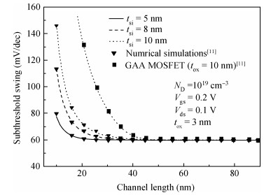

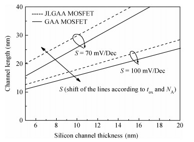


Table 1. Parameters used for MOGA-based computation.

|
Table 2. Optimized nanoscale JLGAA MOSFET design parameters.

|
Table 3. Optimized ultra-low power voltage amplifier design parameters.

|
| [1] |
Djeffal F, Goughali Z, Dibi Z, et al. Analytical analysis of nanoscale multiple gate MOSFETs including effects of hot-carrier induced interface charges. Microelectron Reliab, 2009, 49: 377 doi: 10.1016/j.microrel.2008.12.011
|
| [2] |
Tsompatzoglou A, Dimitriadis C A, Clerc R, et al. Semi-analytical modeling of short-channel effects in Si and Ge symmetrical double-gate MOSFETs. IEEE Trans Electron Devices, 2007, 54: 1943 doi: 10.1109/TED.2007.901075
|
| [3] |
Meguellati M, Djeffal F. New dual-dielectric gate all around (DDGAA) RADFET dosimeter design to improve the radiation sensitivity. Nuclear Instruments and Methods in Physics Research Section A, 2012, 683: 24 doi: 10.1016/j.nima.2012.04.072
|
| [4] |
Bendib T, Djeffal F. Electrical performance optimization of nanoscale double-gate MOSFETs using multi-objective genetic algorithms. IEEE Trans Electron Devices, 2011, 58: 3743 doi: 10.1109/TED.2011.2163820
|
| [5] |
International Technology Roadmap for Semiconductors (ITRS). [Online]. Available: http://public.itrs.net T K Chiang. A new quasi-2-D threshold voltage model for short-channel junctionless cylindrical surrounding gate (JLCSG) MOSFETs. IEEE Trans Electron Devices, 2012, 59: 3127
|
| [6] |
Lee C W, Afzalian A, Akhavan N D, et al. Junctionless multigate field-effect transistor. Appl Phys Lett, 2009, 94: 053511 doi: 10.1063/1.3079411
|
| [7] |
Lee C W, Borne A, Ferain I, et al. High-temperature performance of silicon junctionless MOSFETs. IEEE Trans Electron Devices, 2010, 57: 620 doi: 10.1109/TED.2009.2039093
|
| [8] |
Abd-Elhamid H, Iiguez B, Roig J. Analytical model of the threshold voltage and subthreshold swing of undoped cylindrical gate all around based MOSFETs. IEEE Trans Electronic Devices, 2007, 54(3): 572 doi: 10.1109/TED.2006.890595
|
| [9] |
Su C J, Tsai T I, Liou Y L, et al. Gate-all-around junctionless transistors with heavily doped polysilicon nanowire channels. IEEE Electron Device Lett, 2011, 32(4): 521 doi: 10.1109/LED.2011.2107498
|
| [10] |
Duarte J P, Choi S J, Moon D I, et al. Simple analytical bulk current model for long-channel double-gate junctionless transistors. IEEE Electron Device Lett, 2011, 32: 704 doi: 10.1109/LED.2011.2127441
|
| [11] |
Gnani E, Gnudi A, Reggiani S, et al. Theory of the junctionless nanowire FET. IEEE Trans Electron Devices, 2011, 58: 2903 doi: 10.1109/TED.2011.2159608
|
| [12] |
Chebaki E, Djeffal F, Bentrcia T. Two-dimensional numerical analysis of nanoscale junctionless and double gate MOSFETs including the effect of interfacial traps. Physica Status Solidi C, 2012, 9(10/11): 2041 doi: 10.1002/pssc.201200128/full
|
| [13] |
Atlas User's Manual: Device Simulation Software, 2008
|
| [14] |
Ge L, Fossum J G. Analytical modeling of quantization and volume inversion in thin Si-film DG MOSFETs. IEEE Trans Electron Devices, 2002, 49(2): 287 doi: 10.1109/16.981219
|
| [15] |
Kumar A, Kedzierski J, Laux S E. Quantum-based simulation analysis of scaling in ultrathin body device structures. IEEE Trans Electron Devices, 2005, 52(4): 614 doi: 10.1109/TED.2005.844792
|
| [16] |
Young K K. Analysis of conduction in fully-depleted SOI MOSFETs. IEEE Trans Electron Devices, 1989, 36: 504 doi: 10.1109/16.19960
|
| [17] |
Diagne B, Prégaldiny F, Lallment C, et al. Explicit compact model for symmetric double-gate MOSFETs including solutions for small-geometry effects. Solid-State Electron, 2008, 52: 99 doi: 10.1016/j.sse.2007.06.020
|
| [18] |
Chiang T K. A scaling theory for fully-depleted surrounding-gate MOSFET's: including effective conducting path effect. Microelectron Eng, 2005, 77: 175 doi: 10.1016/j.mee.2004.10.005
|
| [19] |
Djeffal F, Guessasma S, Benhaya A, et al. An analytical approach based on neural computation to estimate the lifetime of deep submicron MOSFETs. Semicond Sci Technol, 2005, 20: 158 doi: 10.1088/0268-1242/20/2/010
|
| [20] |
Bentrcia T, Djeffal F, Chahdi M. An analytical two dimensional subthreshold behavior model to study the nanoscale GCGS DG MOSFET including interfacial trap effects. Microelectron Reliab, 2013, 53(4): 520 doi: 10.1016/j.microrel.2012.12.005
|
| [21] |
Djeffal F, Bendib T, Abdi M A. A two-dimensional semi-analytical analysis of the subthreshold-swing behavior including free carriers and interfacial traps effects for nanoscale double-gate MOSFETs. J Microelectron, 2011, 42: 1391 doi: 10.1016/j.mejo.2011.09.008
|
| [22] |
Djeffal F, Bendib T. Multi-objective genetic algorithms based approach to optimize the electrical performances of the gate stack double gate (GSDG) MOSFET. Microelectron J, 2011, 42: 661 doi: 10.1016/j.mejo.2011.03.003
|
| [23] |
Chen Z, Xiao Y, Tang M, et al. Surface-potential-based drain current model for long-channel junctionless double-gate MOSFETs. IEEE Trans Electron Devices, 2012, 59: 3292 doi: 10.1109/TED.2012.2221164
|
| [24] |
Atashkari K, Nariman-Zadeh N, Pilechi A, et al. Thermodynamic pareto optimization of turbojet engines using multiobjective genetic algorithms. Int J Thermal Sci, 2005, 44: 1061 doi: 10.1016/j.ijthermalsci.2005.03.016
|
| [25] |
Chang P C, Hsieh J C, Wang C Y. Adaptive multi-objective genetic algorithms for scheduling of drilling operation in printed circuit board industry. Appl Soft Comput, 2007, 7: 800 doi: 10.1016/j.asoc.2006.02.002
|
| [26] |
Meguellati M, Djeffal F, Arar D, et al. New RADFET dosimeter design for radioactive environment monitoring applications. Eng Lett, 2012, 20: 339 http://connection.ebscohost.com/c/articles/85783793/new-radfet-dosimeter-design-radioactive-environment-monitoring-applications
|
| [27] |
Abdi M A, Djeffal F, Meguellati M, et al. Two-dimensional analytical threshold voltage model for nanoscale graded channel gate stack DG MOSFETs. 16th IEEE International Conference on Electronics, Circuits and Systems, ICECS, 2009: 892 http://ieeexplore.ieee.org/xpls/icp.jsp?arnumber=5410801
|
| [28] |
Wang A, Chandrakasan A. A 180 mV subthreshold FFT processor using a minimum energy design methodology. IEEE J Solid-State Circuits, 2005, 40: 310 doi: 10.1109/JSSC.2004.837945
|


Article views: 2371 Times PDF downloads: 29 Times Cited by: 0 Times
Received: 23 December 2013 Revised: 30 January 2014 Online: Published: 01 July 2014
| Citation: |
T. Bendib, F. Djeffal, M. Meguellati. An optimized junctionless GAA MOSFET design based on multi-objective computation for high-performance ultra-low power devices[J]. Journal of Semiconductors, 2014, 35(7): 074002. doi: 10.1088/1674-4926/35/7/074002
T. Bendib, F. Djeffal, M. Meguellati. An optimized junctionless GAA MOSFET design based on multi-objective computation for high-performance ultra-low power devices[J]. J. Semicond., 2014, 35(7): 074002. doi: 10.1088/1674-4926/35/7/074002.
Export: BibTex EndNote

|
| [1] |
Djeffal F, Goughali Z, Dibi Z, et al. Analytical analysis of nanoscale multiple gate MOSFETs including effects of hot-carrier induced interface charges. Microelectron Reliab, 2009, 49: 377 doi: 10.1016/j.microrel.2008.12.011
|
| [2] |
Tsompatzoglou A, Dimitriadis C A, Clerc R, et al. Semi-analytical modeling of short-channel effects in Si and Ge symmetrical double-gate MOSFETs. IEEE Trans Electron Devices, 2007, 54: 1943 doi: 10.1109/TED.2007.901075
|
| [3] |
Meguellati M, Djeffal F. New dual-dielectric gate all around (DDGAA) RADFET dosimeter design to improve the radiation sensitivity. Nuclear Instruments and Methods in Physics Research Section A, 2012, 683: 24 doi: 10.1016/j.nima.2012.04.072
|
| [4] |
Bendib T, Djeffal F. Electrical performance optimization of nanoscale double-gate MOSFETs using multi-objective genetic algorithms. IEEE Trans Electron Devices, 2011, 58: 3743 doi: 10.1109/TED.2011.2163820
|
| [5] |
International Technology Roadmap for Semiconductors (ITRS). [Online]. Available: http://public.itrs.net T K Chiang. A new quasi-2-D threshold voltage model for short-channel junctionless cylindrical surrounding gate (JLCSG) MOSFETs. IEEE Trans Electron Devices, 2012, 59: 3127
|
| [6] |
Lee C W, Afzalian A, Akhavan N D, et al. Junctionless multigate field-effect transistor. Appl Phys Lett, 2009, 94: 053511 doi: 10.1063/1.3079411
|
| [7] |
Lee C W, Borne A, Ferain I, et al. High-temperature performance of silicon junctionless MOSFETs. IEEE Trans Electron Devices, 2010, 57: 620 doi: 10.1109/TED.2009.2039093
|
| [8] |
Abd-Elhamid H, Iiguez B, Roig J. Analytical model of the threshold voltage and subthreshold swing of undoped cylindrical gate all around based MOSFETs. IEEE Trans Electronic Devices, 2007, 54(3): 572 doi: 10.1109/TED.2006.890595
|
| [9] |
Su C J, Tsai T I, Liou Y L, et al. Gate-all-around junctionless transistors with heavily doped polysilicon nanowire channels. IEEE Electron Device Lett, 2011, 32(4): 521 doi: 10.1109/LED.2011.2107498
|
| [10] |
Duarte J P, Choi S J, Moon D I, et al. Simple analytical bulk current model for long-channel double-gate junctionless transistors. IEEE Electron Device Lett, 2011, 32: 704 doi: 10.1109/LED.2011.2127441
|
| [11] |
Gnani E, Gnudi A, Reggiani S, et al. Theory of the junctionless nanowire FET. IEEE Trans Electron Devices, 2011, 58: 2903 doi: 10.1109/TED.2011.2159608
|
| [12] |
Chebaki E, Djeffal F, Bentrcia T. Two-dimensional numerical analysis of nanoscale junctionless and double gate MOSFETs including the effect of interfacial traps. Physica Status Solidi C, 2012, 9(10/11): 2041 doi: 10.1002/pssc.201200128/full
|
| [13] |
Atlas User's Manual: Device Simulation Software, 2008
|
| [14] |
Ge L, Fossum J G. Analytical modeling of quantization and volume inversion in thin Si-film DG MOSFETs. IEEE Trans Electron Devices, 2002, 49(2): 287 doi: 10.1109/16.981219
|
| [15] |
Kumar A, Kedzierski J, Laux S E. Quantum-based simulation analysis of scaling in ultrathin body device structures. IEEE Trans Electron Devices, 2005, 52(4): 614 doi: 10.1109/TED.2005.844792
|
| [16] |
Young K K. Analysis of conduction in fully-depleted SOI MOSFETs. IEEE Trans Electron Devices, 1989, 36: 504 doi: 10.1109/16.19960
|
| [17] |
Diagne B, Prégaldiny F, Lallment C, et al. Explicit compact model for symmetric double-gate MOSFETs including solutions for small-geometry effects. Solid-State Electron, 2008, 52: 99 doi: 10.1016/j.sse.2007.06.020
|
| [18] |
Chiang T K. A scaling theory for fully-depleted surrounding-gate MOSFET's: including effective conducting path effect. Microelectron Eng, 2005, 77: 175 doi: 10.1016/j.mee.2004.10.005
|
| [19] |
Djeffal F, Guessasma S, Benhaya A, et al. An analytical approach based on neural computation to estimate the lifetime of deep submicron MOSFETs. Semicond Sci Technol, 2005, 20: 158 doi: 10.1088/0268-1242/20/2/010
|
| [20] |
Bentrcia T, Djeffal F, Chahdi M. An analytical two dimensional subthreshold behavior model to study the nanoscale GCGS DG MOSFET including interfacial trap effects. Microelectron Reliab, 2013, 53(4): 520 doi: 10.1016/j.microrel.2012.12.005
|
| [21] |
Djeffal F, Bendib T, Abdi M A. A two-dimensional semi-analytical analysis of the subthreshold-swing behavior including free carriers and interfacial traps effects for nanoscale double-gate MOSFETs. J Microelectron, 2011, 42: 1391 doi: 10.1016/j.mejo.2011.09.008
|
| [22] |
Djeffal F, Bendib T. Multi-objective genetic algorithms based approach to optimize the electrical performances of the gate stack double gate (GSDG) MOSFET. Microelectron J, 2011, 42: 661 doi: 10.1016/j.mejo.2011.03.003
|
| [23] |
Chen Z, Xiao Y, Tang M, et al. Surface-potential-based drain current model for long-channel junctionless double-gate MOSFETs. IEEE Trans Electron Devices, 2012, 59: 3292 doi: 10.1109/TED.2012.2221164
|
| [24] |
Atashkari K, Nariman-Zadeh N, Pilechi A, et al. Thermodynamic pareto optimization of turbojet engines using multiobjective genetic algorithms. Int J Thermal Sci, 2005, 44: 1061 doi: 10.1016/j.ijthermalsci.2005.03.016
|
| [25] |
Chang P C, Hsieh J C, Wang C Y. Adaptive multi-objective genetic algorithms for scheduling of drilling operation in printed circuit board industry. Appl Soft Comput, 2007, 7: 800 doi: 10.1016/j.asoc.2006.02.002
|
| [26] |
Meguellati M, Djeffal F, Arar D, et al. New RADFET dosimeter design for radioactive environment monitoring applications. Eng Lett, 2012, 20: 339 http://connection.ebscohost.com/c/articles/85783793/new-radfet-dosimeter-design-radioactive-environment-monitoring-applications
|
| [27] |
Abdi M A, Djeffal F, Meguellati M, et al. Two-dimensional analytical threshold voltage model for nanoscale graded channel gate stack DG MOSFETs. 16th IEEE International Conference on Electronics, Circuits and Systems, ICECS, 2009: 892 http://ieeexplore.ieee.org/xpls/icp.jsp?arnumber=5410801
|
| [28] |
Wang A, Chandrakasan A. A 180 mV subthreshold FFT processor using a minimum energy design methodology. IEEE J Solid-State Circuits, 2005, 40: 310 doi: 10.1109/JSSC.2004.837945
|

 WeChat ID
Journal of Semiconductors © 2017 All Rights Reserved 京ICP备05085259号-2

 DownLoad:

