Issue Browser
Volume 43, Issue 6,
Jun 2022
Column
J. Semicond.
2022, 43(6): 061101 doi: 10.1088/1674-4926/43/6/061101
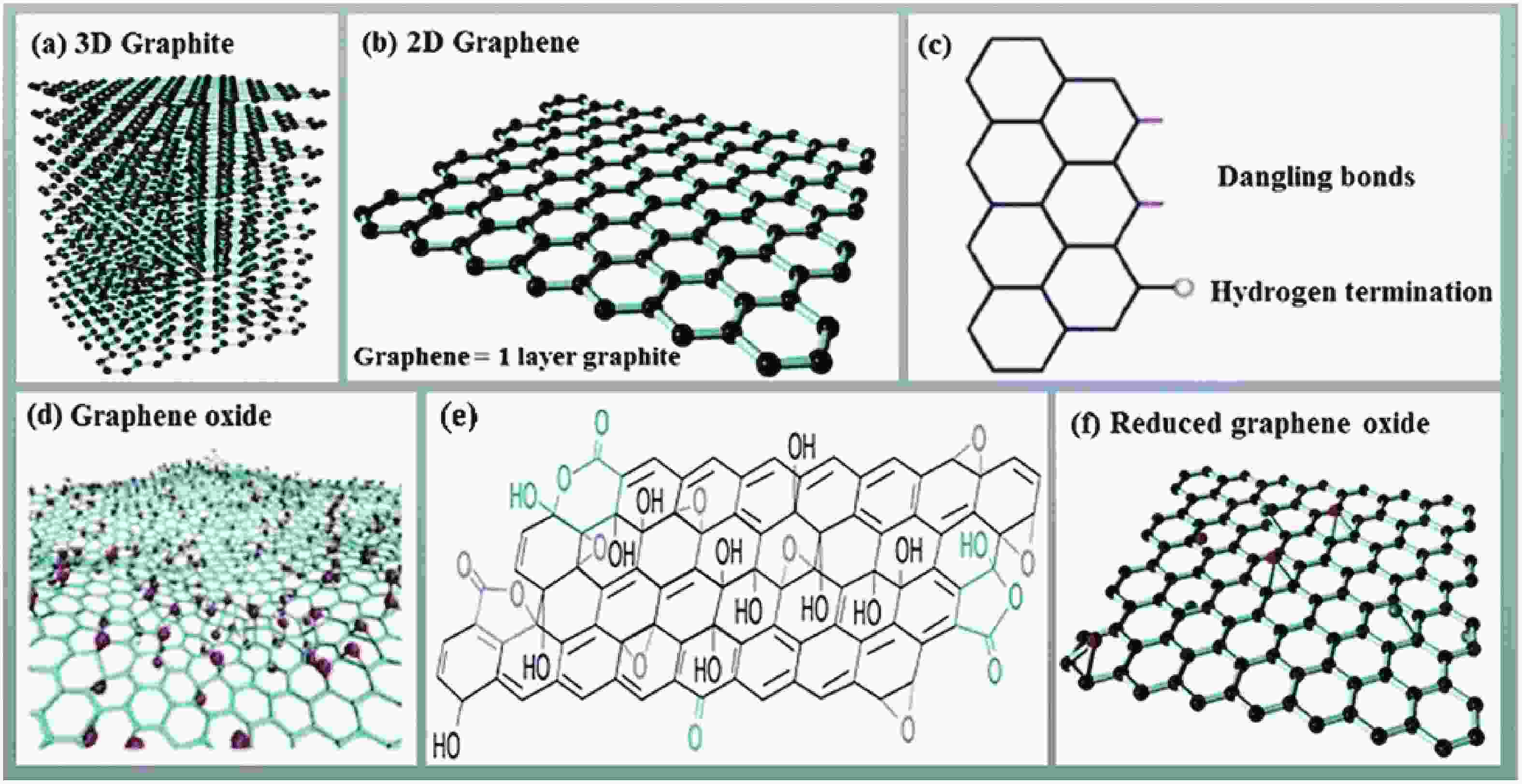
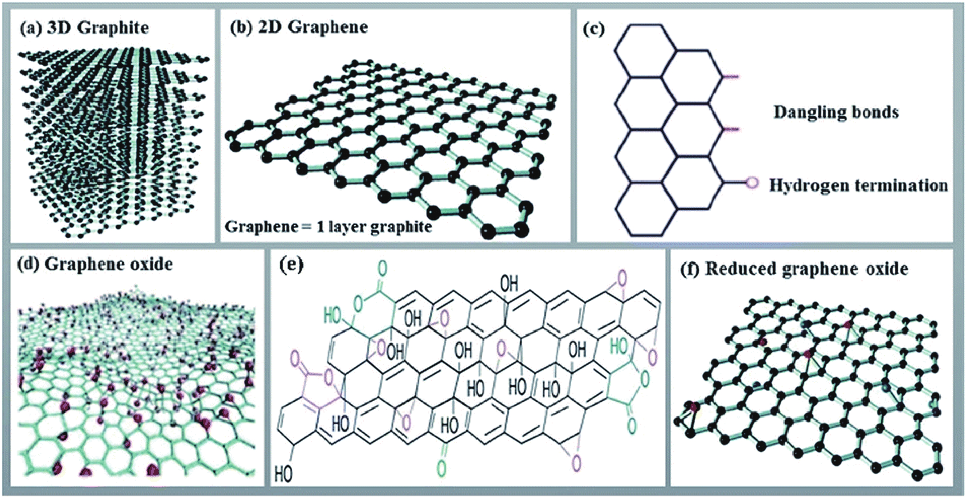
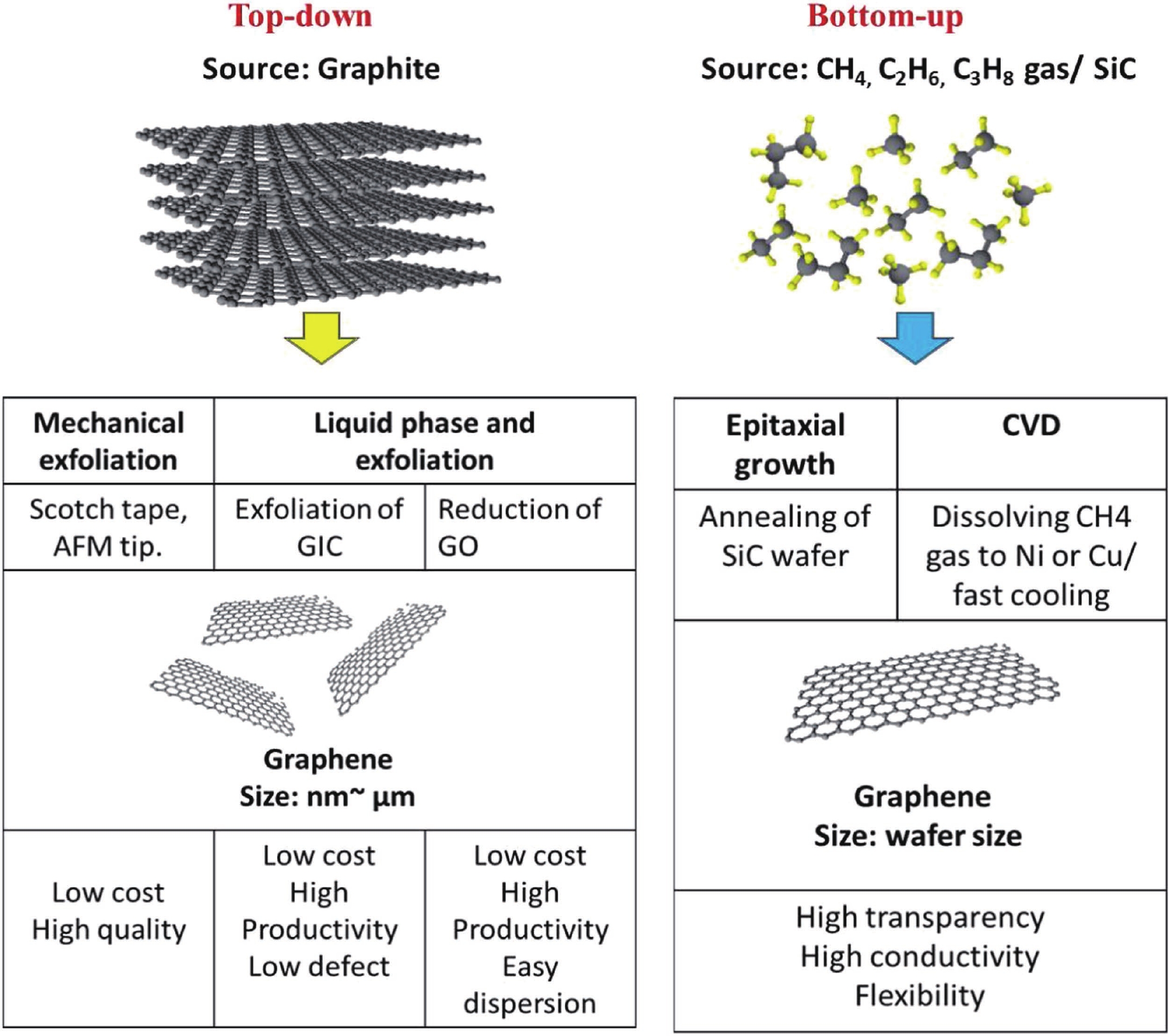
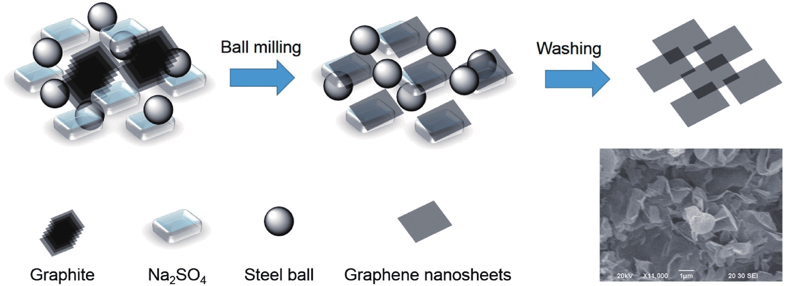
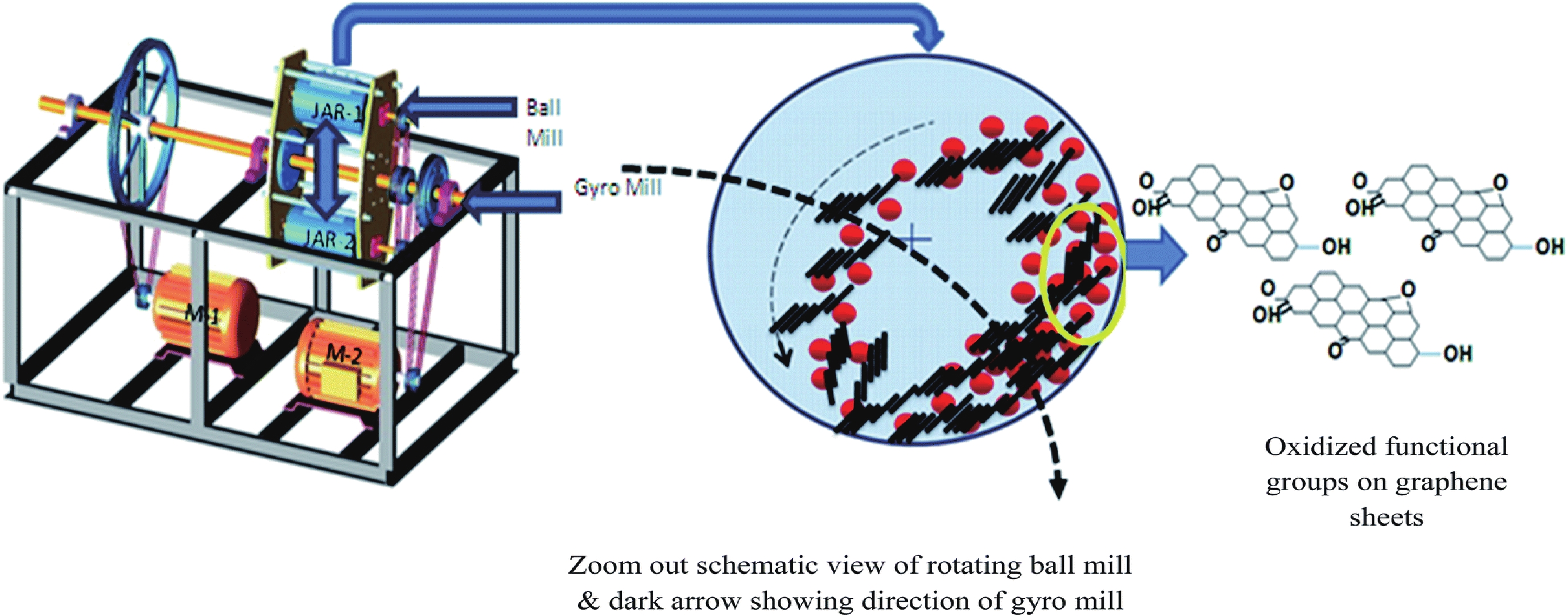
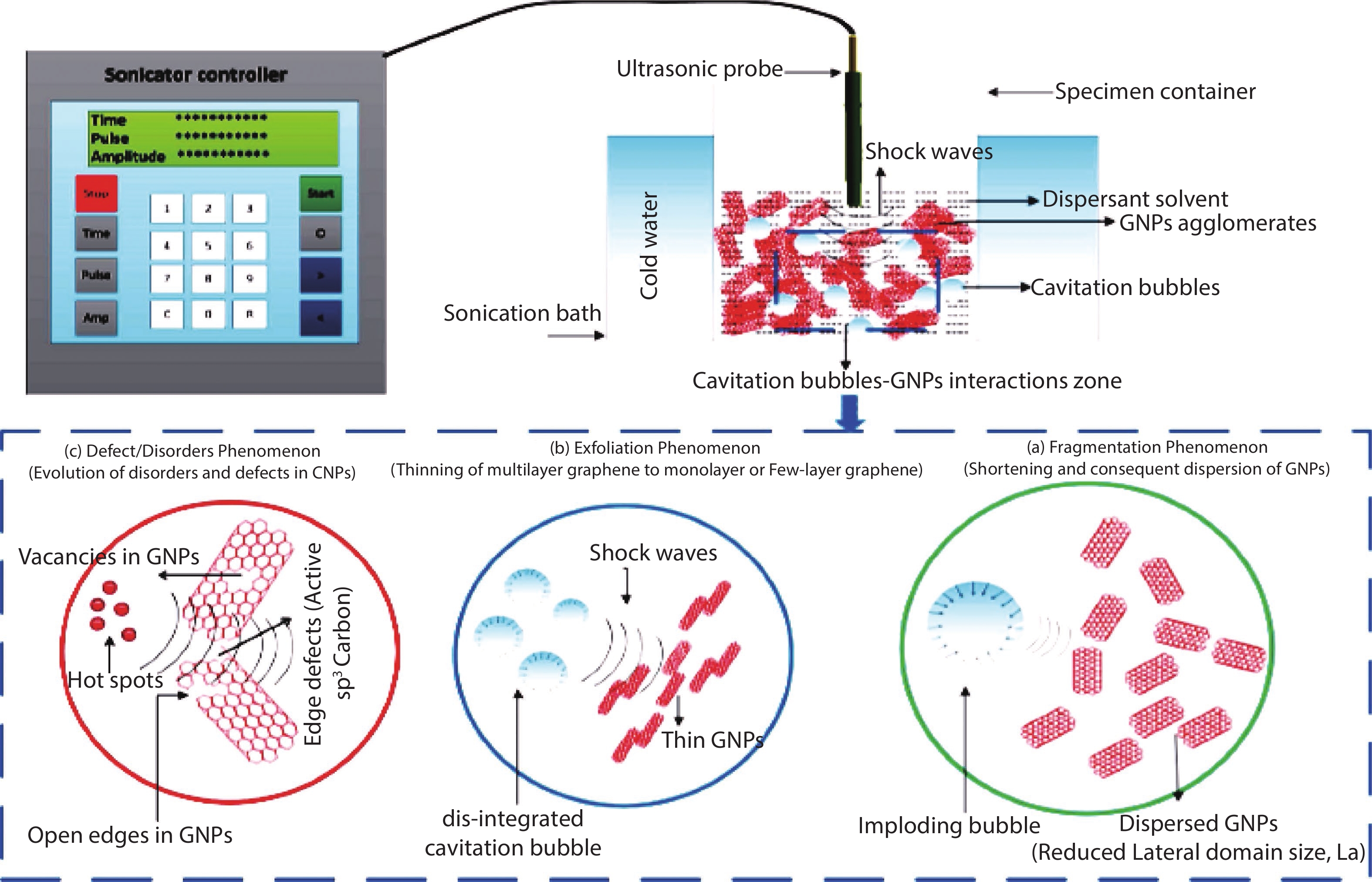
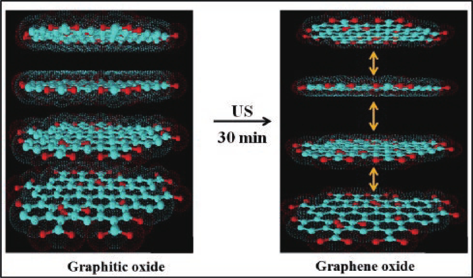
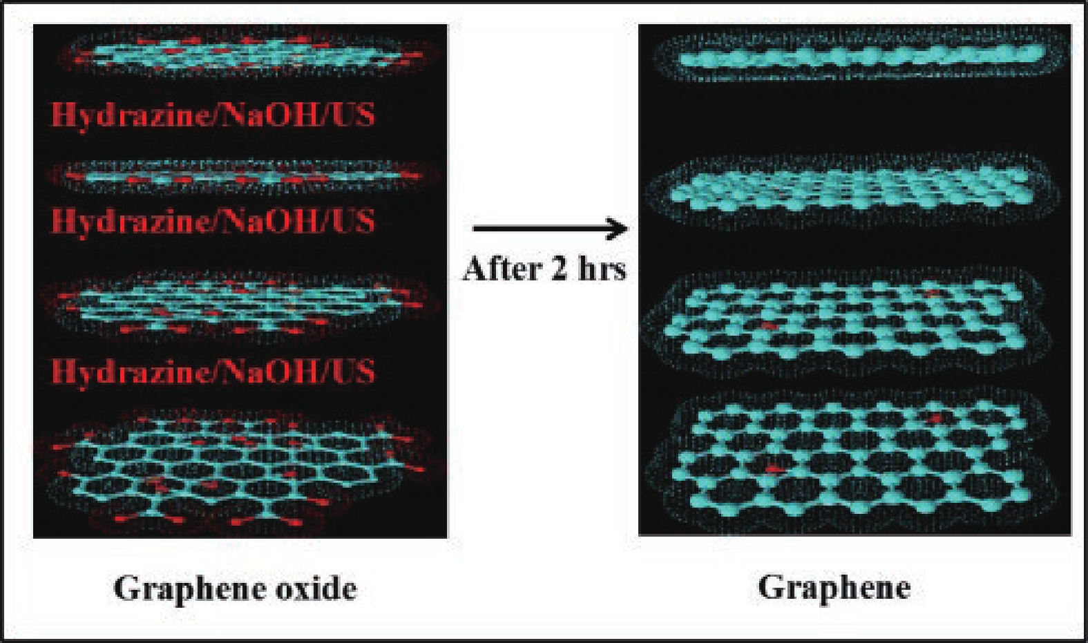
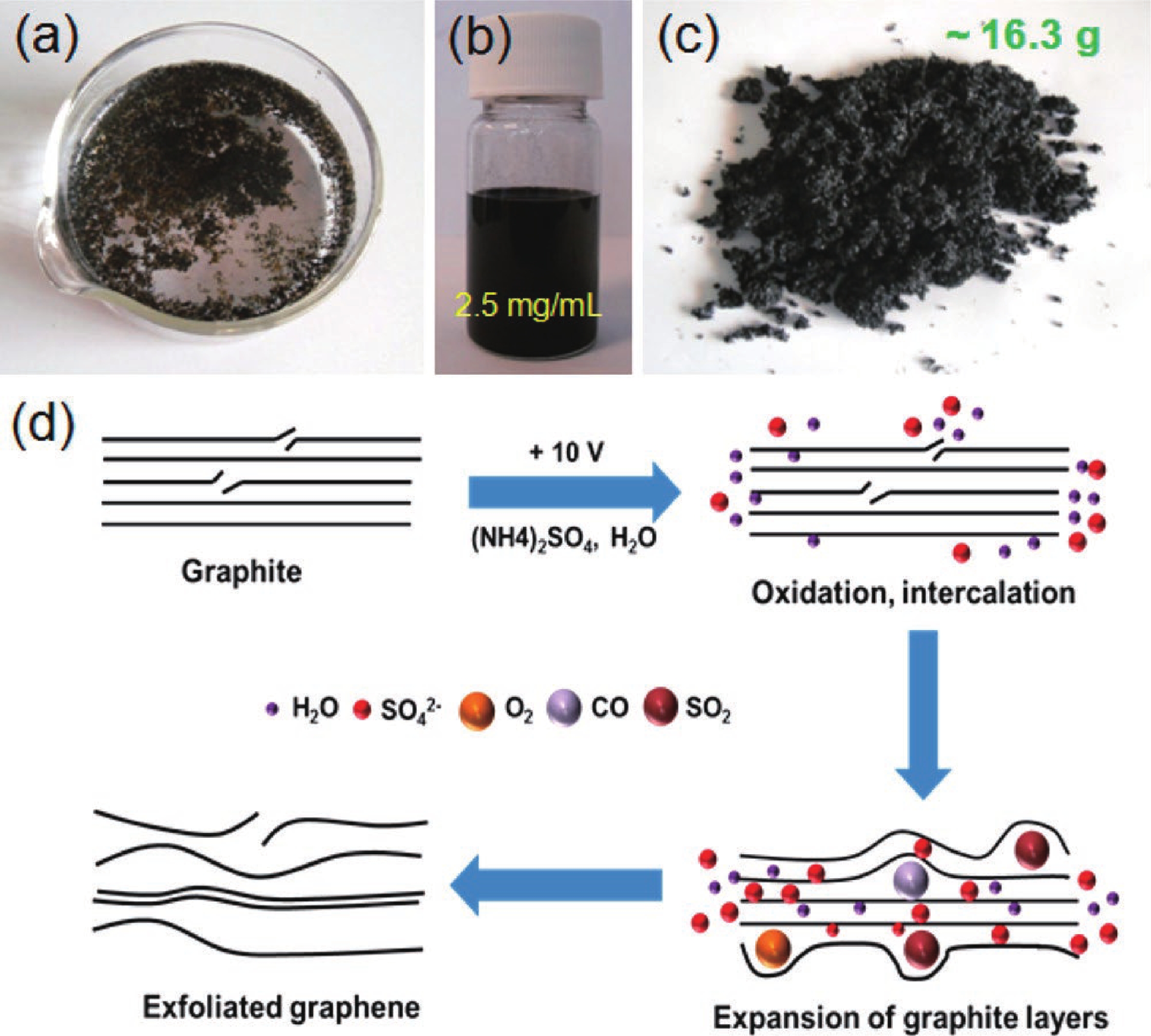
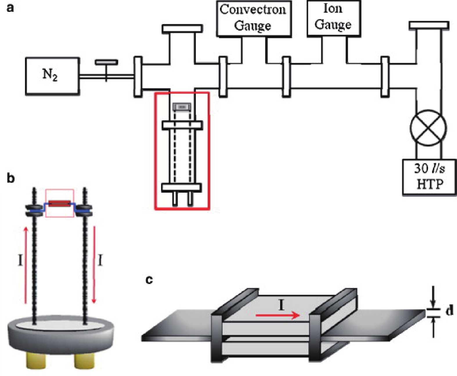
This study presents an overview on graphene synthesis, fabrication and different characterization techniques utilized in the production. Since its discovery in 2004 by Andre Geim and Kostya Novoselov several research articles have been published globally to this effect, owing to graphene’s extraordinary, and exclusive characteristics which include optical transparency, excellent thermal, and mechanical properties. The properties and applications of this two-dimensional carbon crystal composed of single-layered material have created new avenues for the development of high-performance future electronics and technologies in energy storage and conversion for the sustainable energy. However, despite its potential and current status globally the difficulty in the production of monolayer graphene sheet still persists. Therefore, this review highlighted two approaches in the synthesis of graphene, which are the top-down and bottom-up approaches and examined the advantages and failings of the methods involved. In addition, the prospects and failings of these methods are investigated, as they are essential in optimizing the production method of graphene vital for expanding the yield, and producing high-quality graphene.


J. Semicond.
2022, 43(6): 063101 doi: 10.1088/1674-4926/43/6/063101
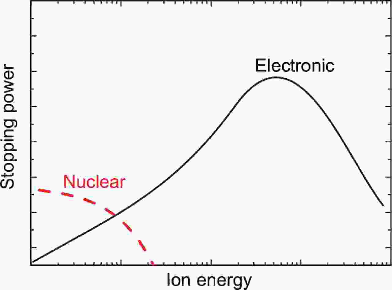
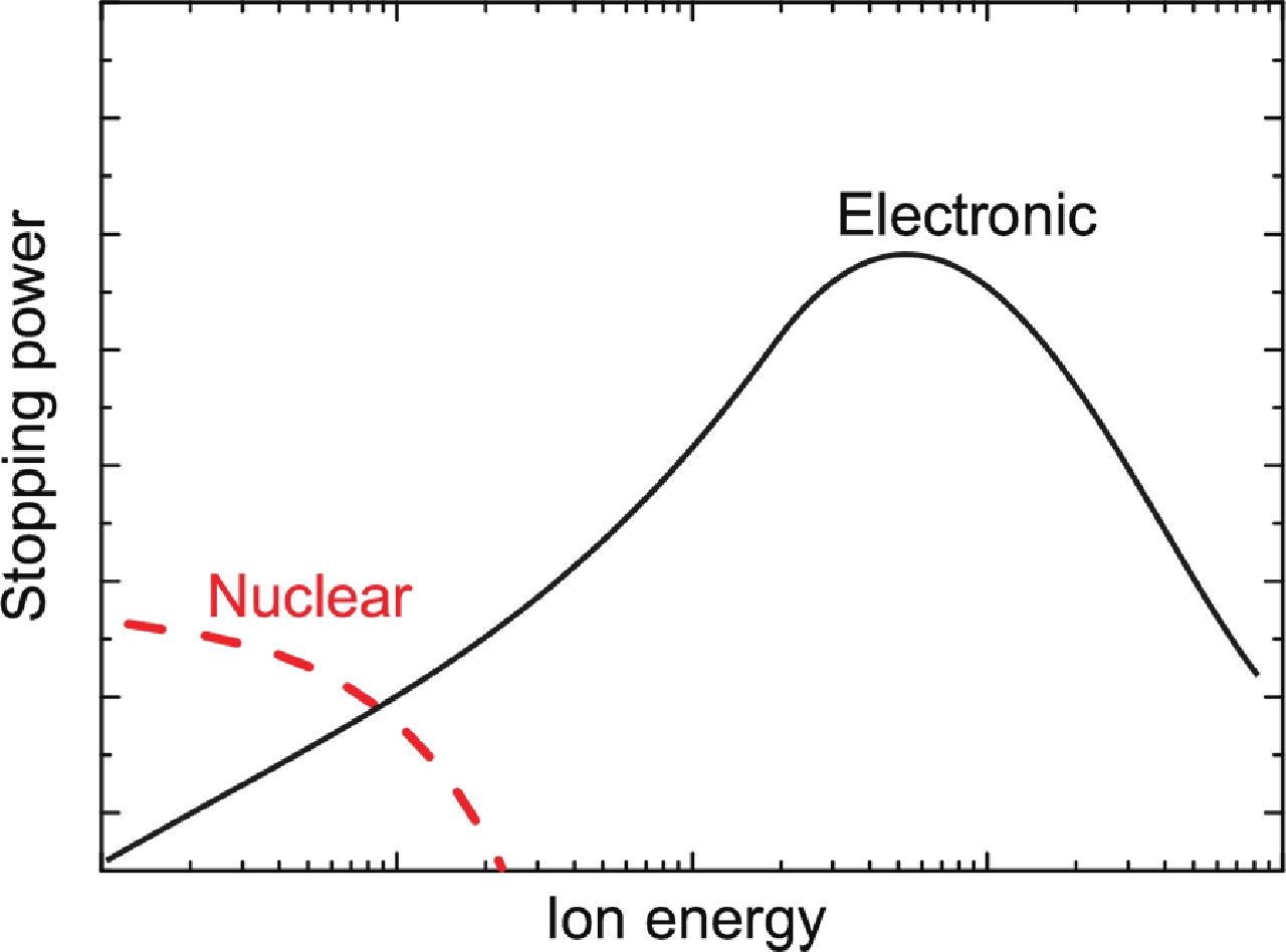
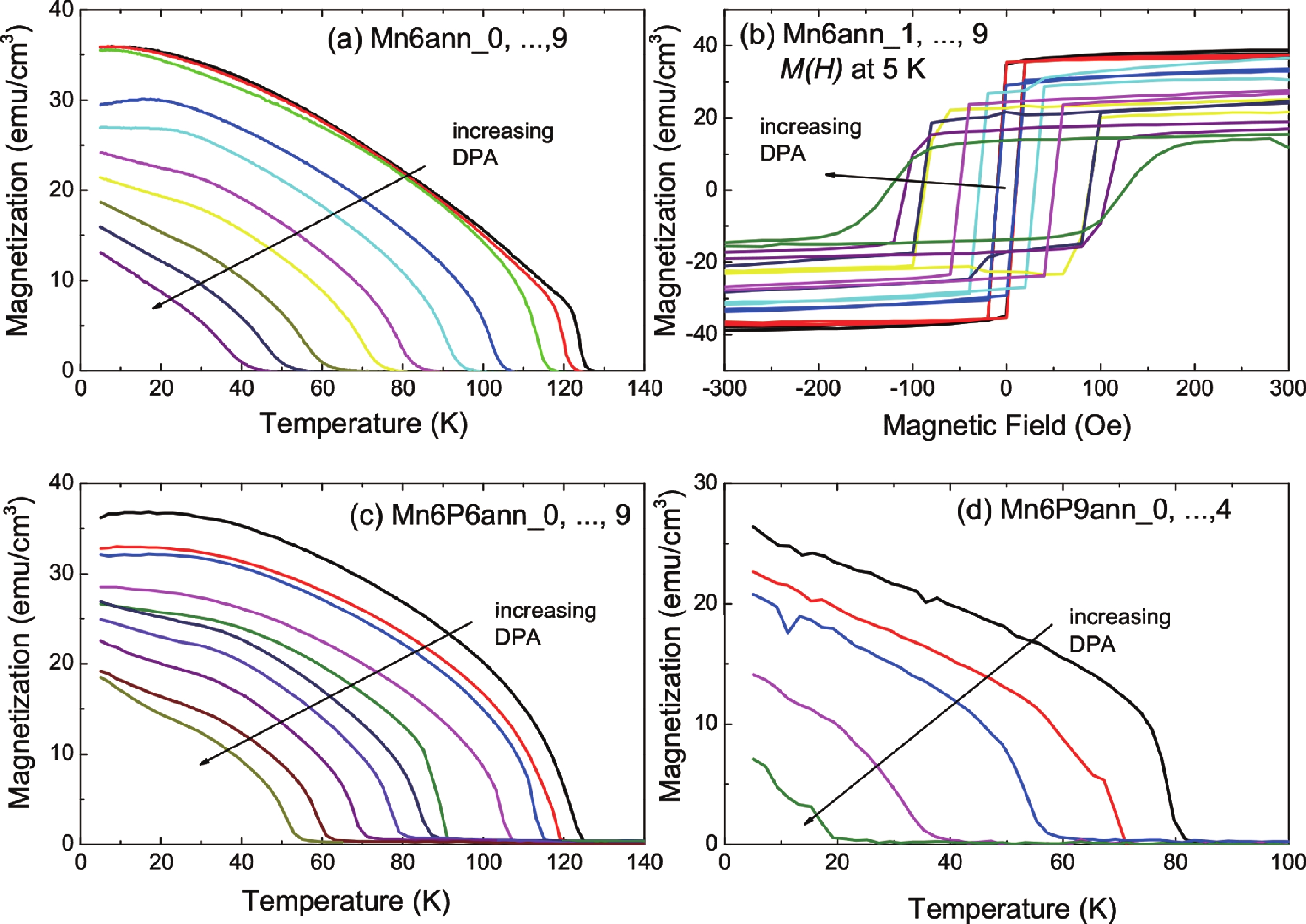
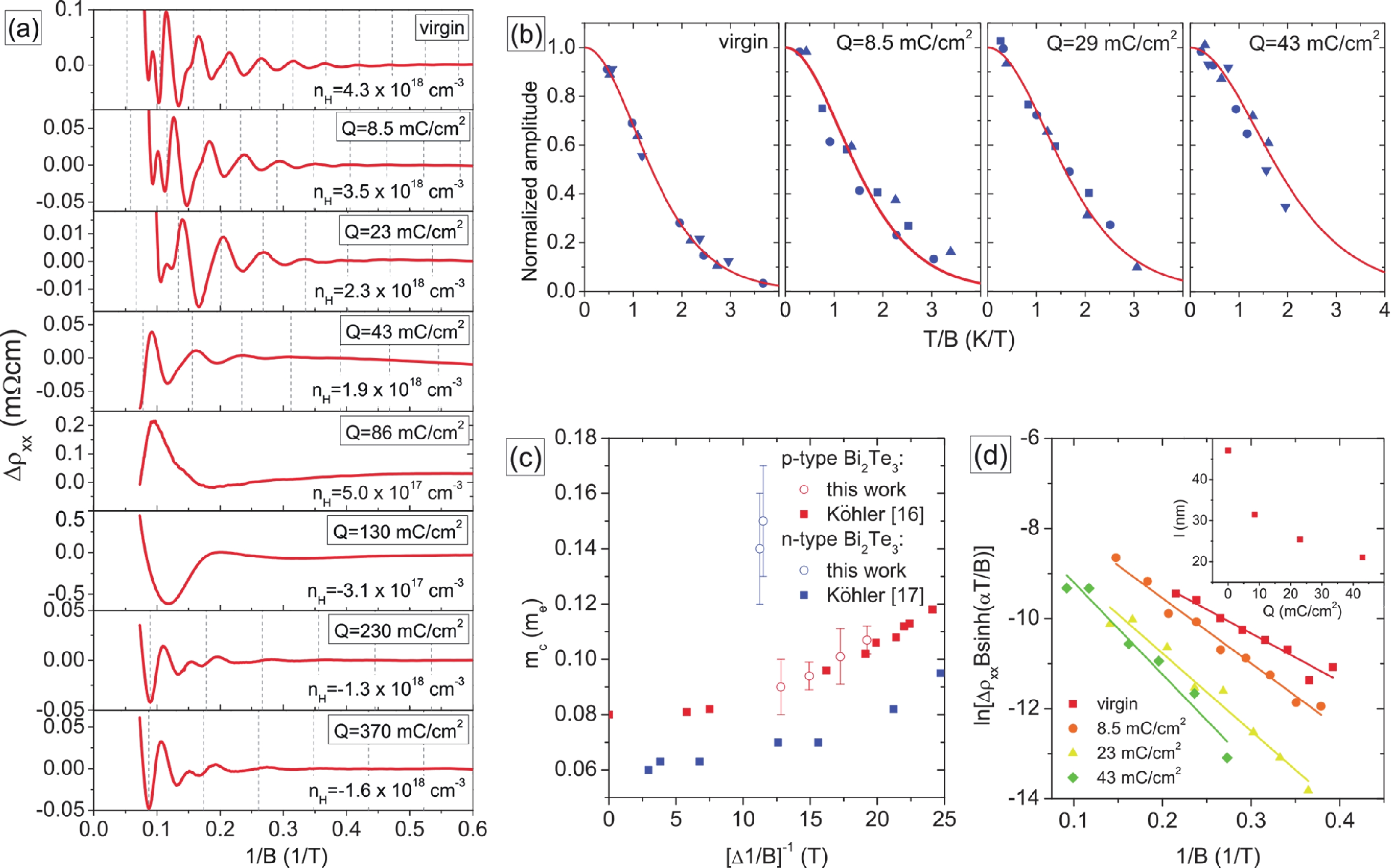
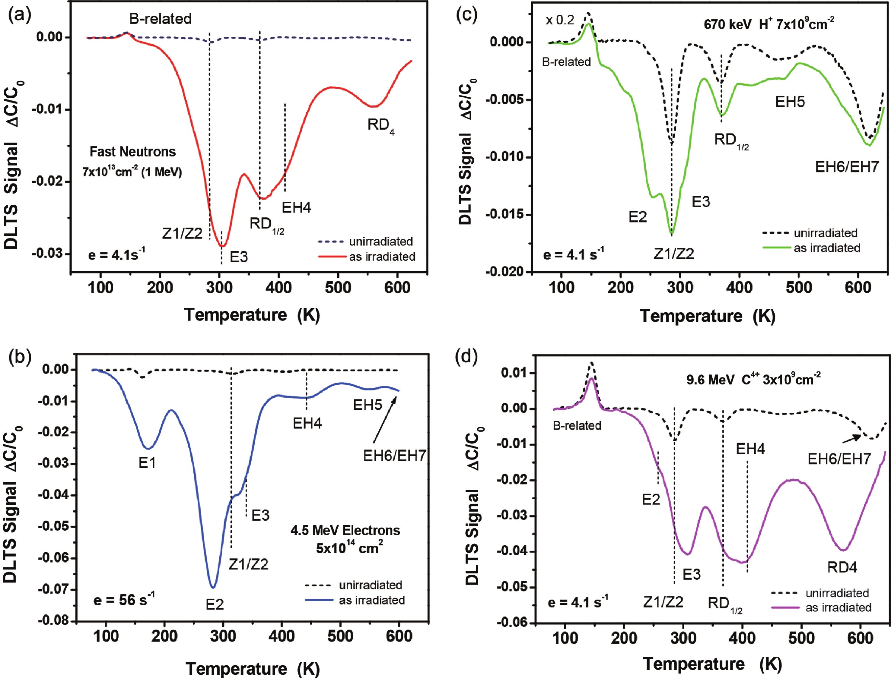
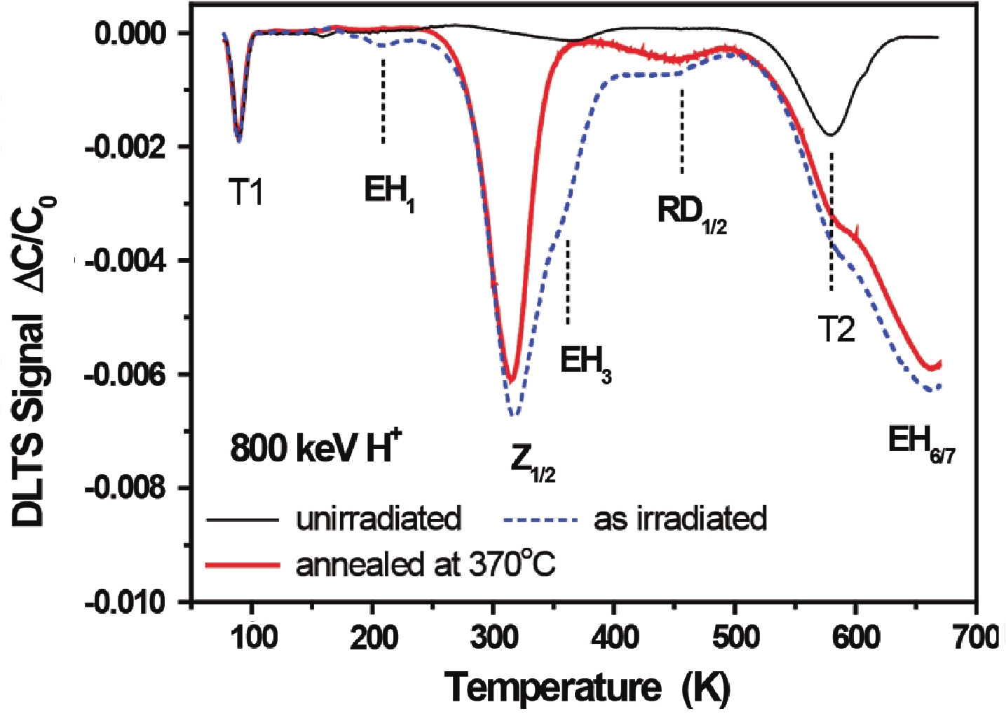
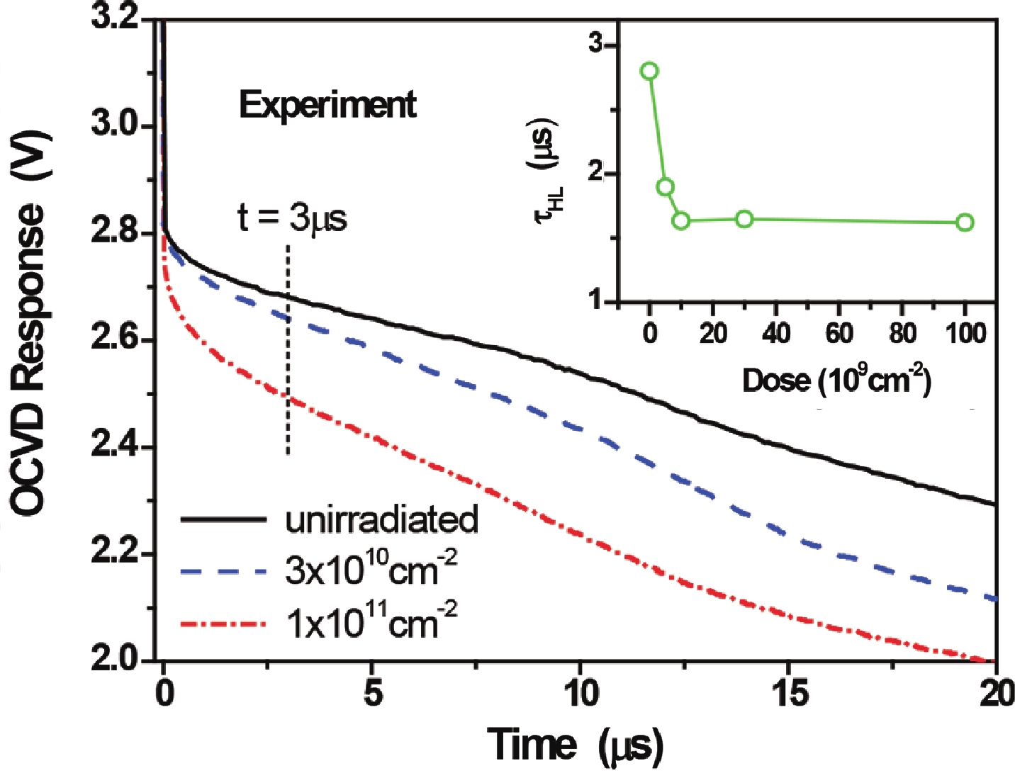
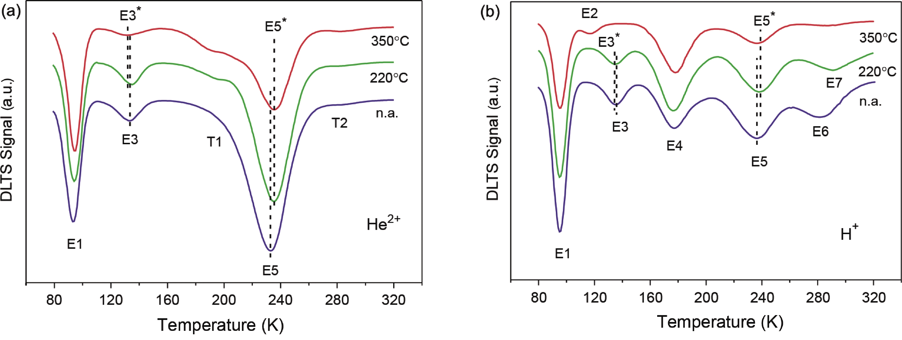
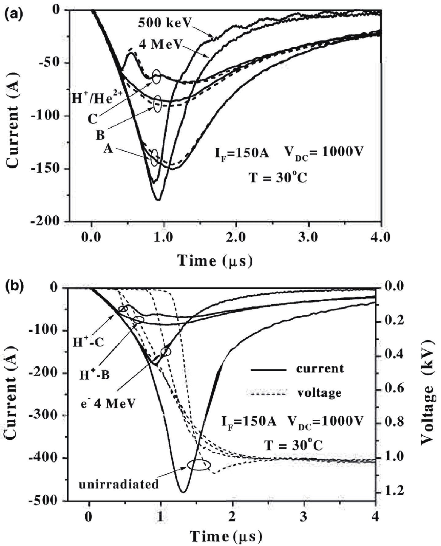
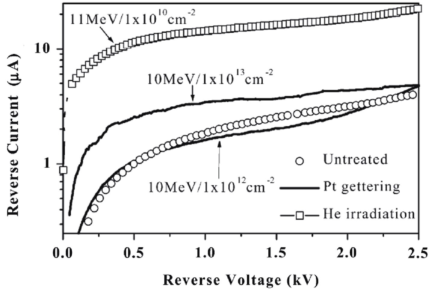
In this review, the application of light ion irradiation is discussed for tailoring novel functional materials and for improving the performance in SiC or Si based electrical power devices. The deep traps and electronic disorder produced by light ion irradiation can modify the electrical, magnetic, and optical properties of films (e.g., dilute ferromagnetic semiconductors and topological materials). Additionally, benefiting from the high reproducibility, precise manipulation of functional depth and density of defects, as well as the flexible patternability, the helium or proton ion irradiation has been successfully employed in improving the dynamic performance of SiC and Si based PiN diode power devices by reducing their majority carrier lifetime, although the static performance is sacrificed due to deep level traps. Such a trade-off has been regarded as the key point to compromise the static and dynamic performances of power devices. As a result, herein the light ion irradiation is highlighted in both exploring new physics and optimizing the performance in functional materials and electrical devices.


J. Semicond.
2022, 43(6): 062302 doi: 10.1088/1674-4926/43/6/062302

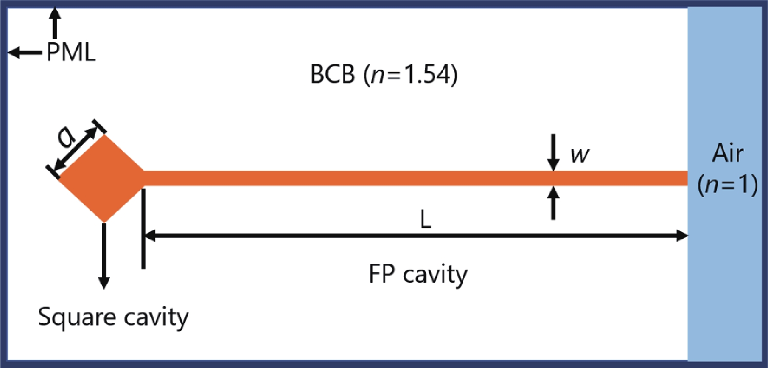
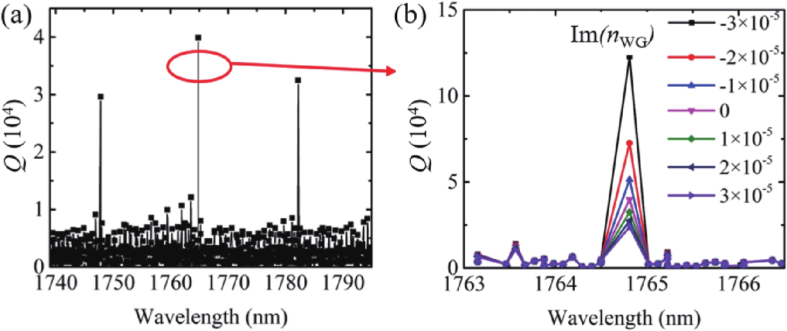
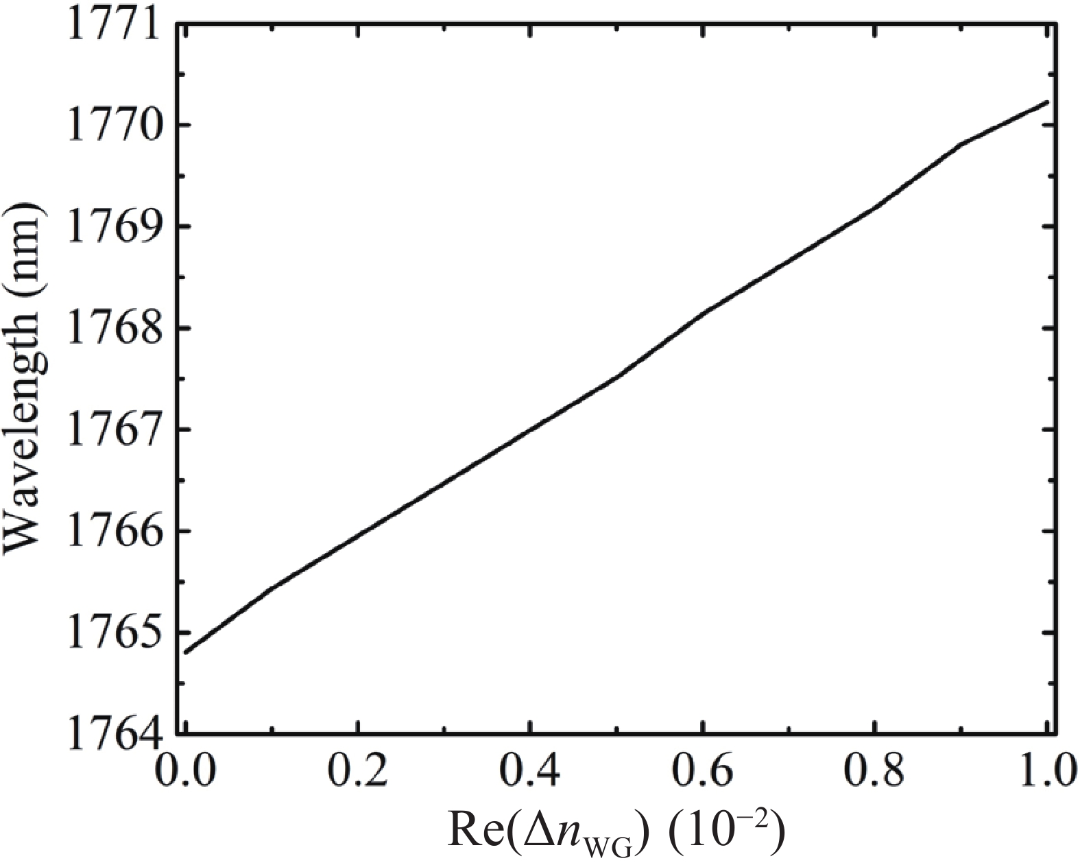
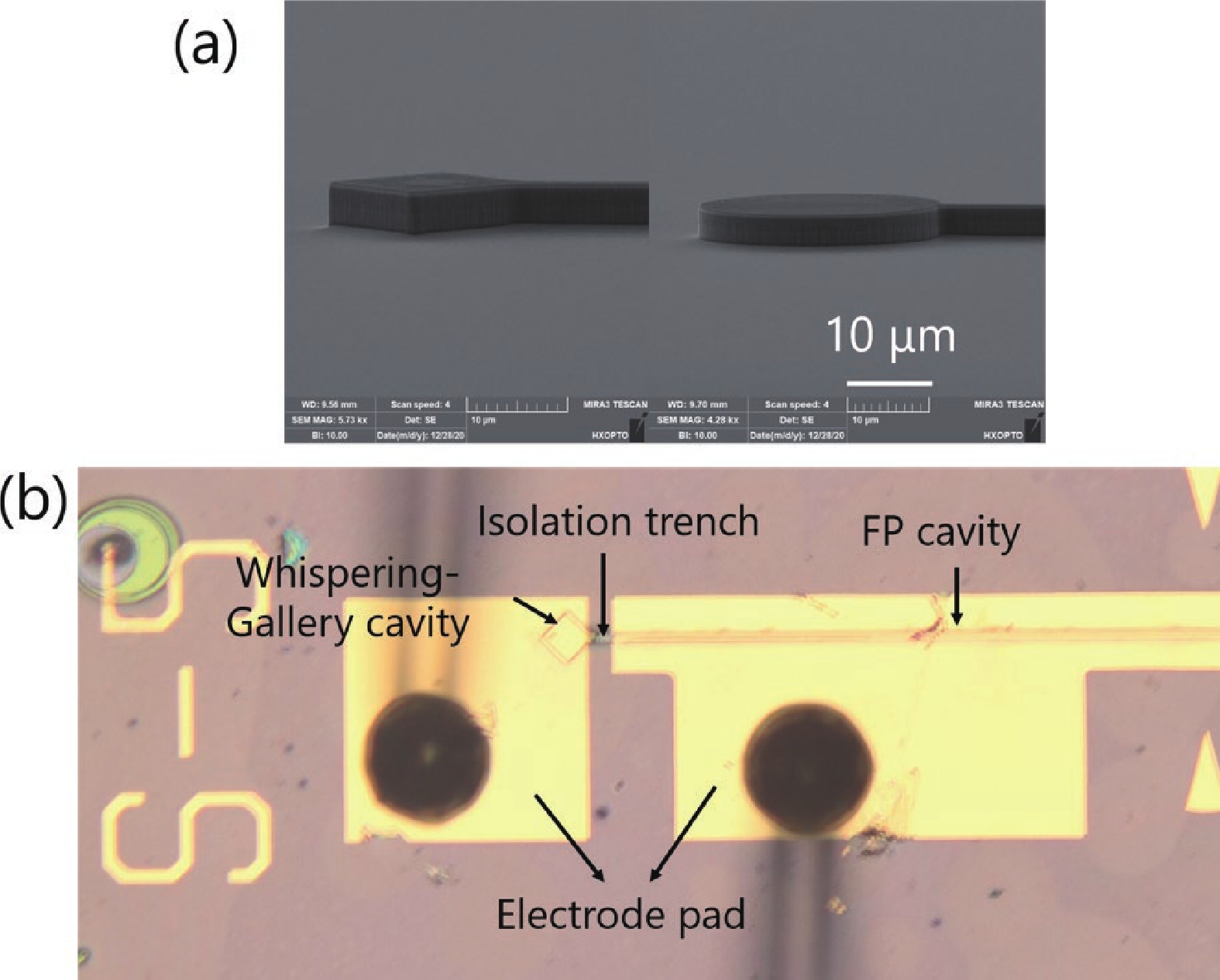
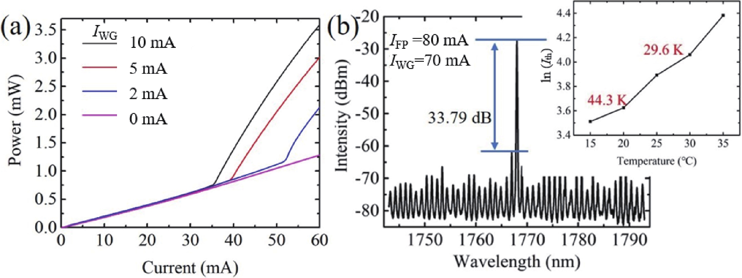
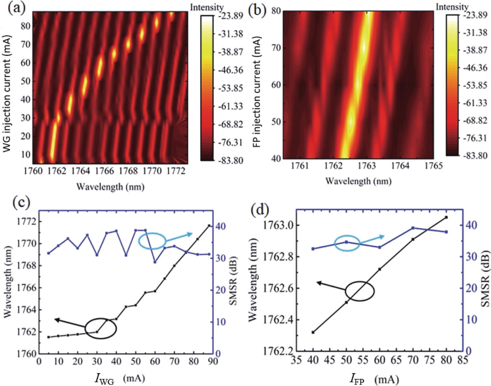
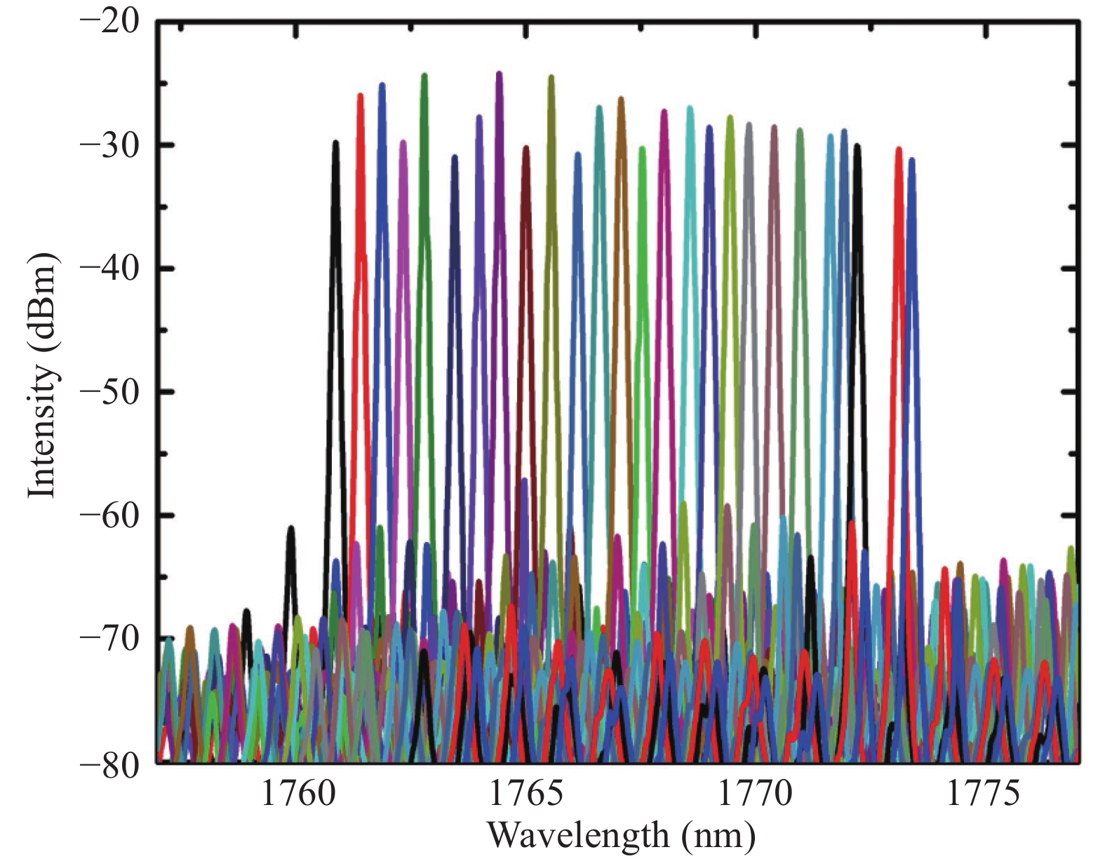
A wide wavelength tuning range and single-mode hybrid cavity laser consists of a square Whispering-Gallery (WG) microcavity and a Fabry–Pérot (FP) was introduced and demonstrated. A wavelength tuning range over 12.5 nm from 1760.87 to 1773.39 nm which was single-mode emitting was obtained with the side-mode suppression ratio over 30 dB. The hybrid cavity laser does not need grating etching and special epitaxial structure, which reduces the fabrication difficulty and cost, and shows the potential for gas sensing with absorption lines in this range.
J. Semicond.
2022, 43(6): 062303 doi: 10.1088/1674-4926/43/6/062303

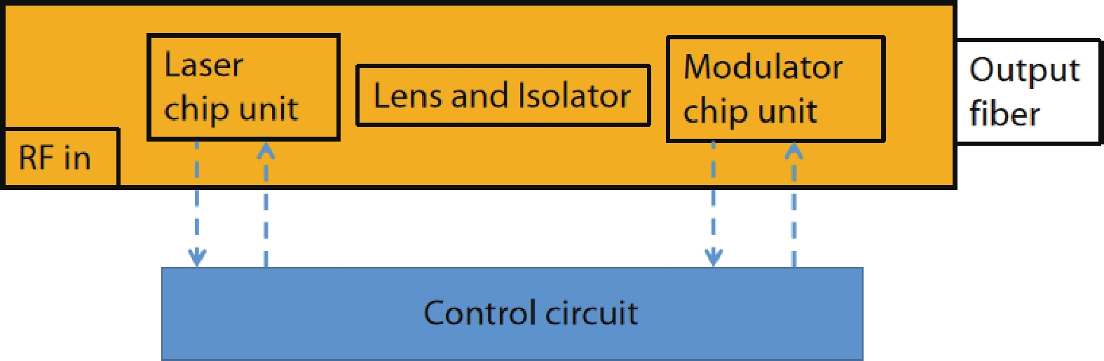
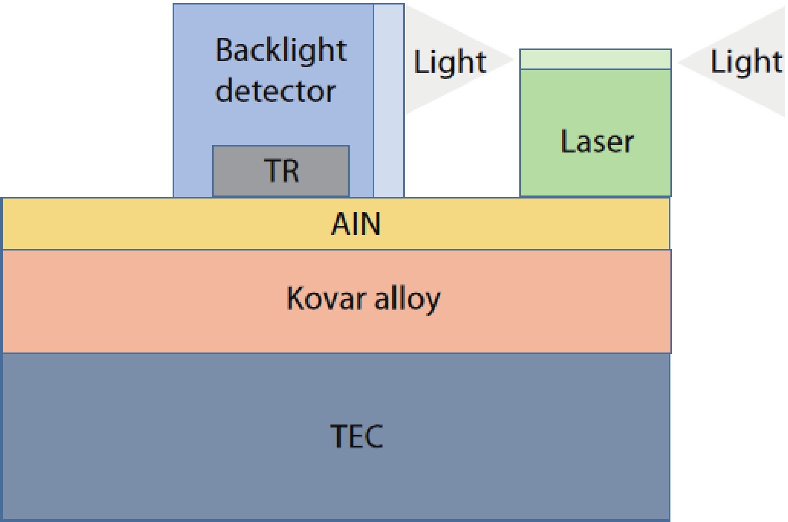
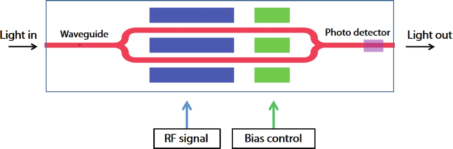
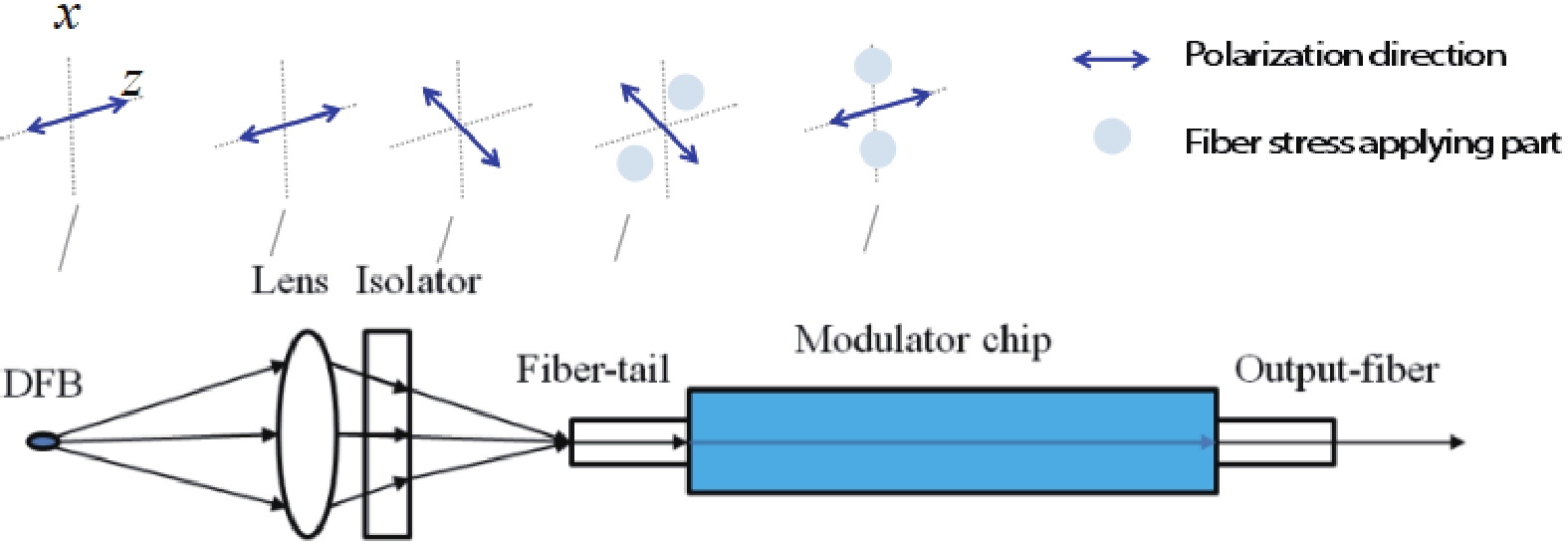
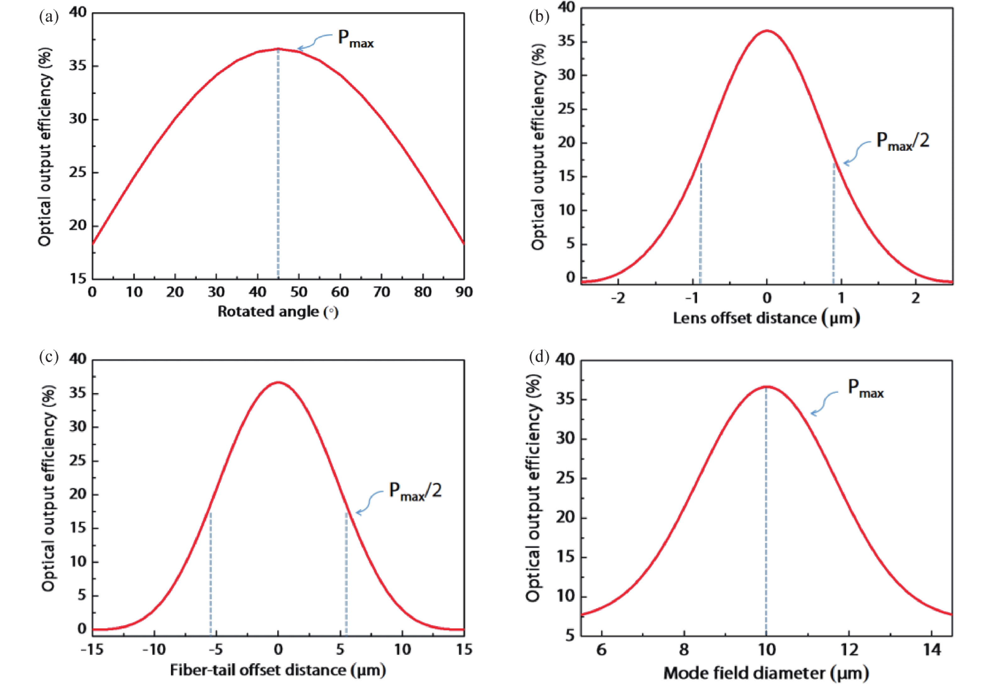
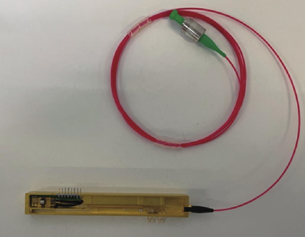
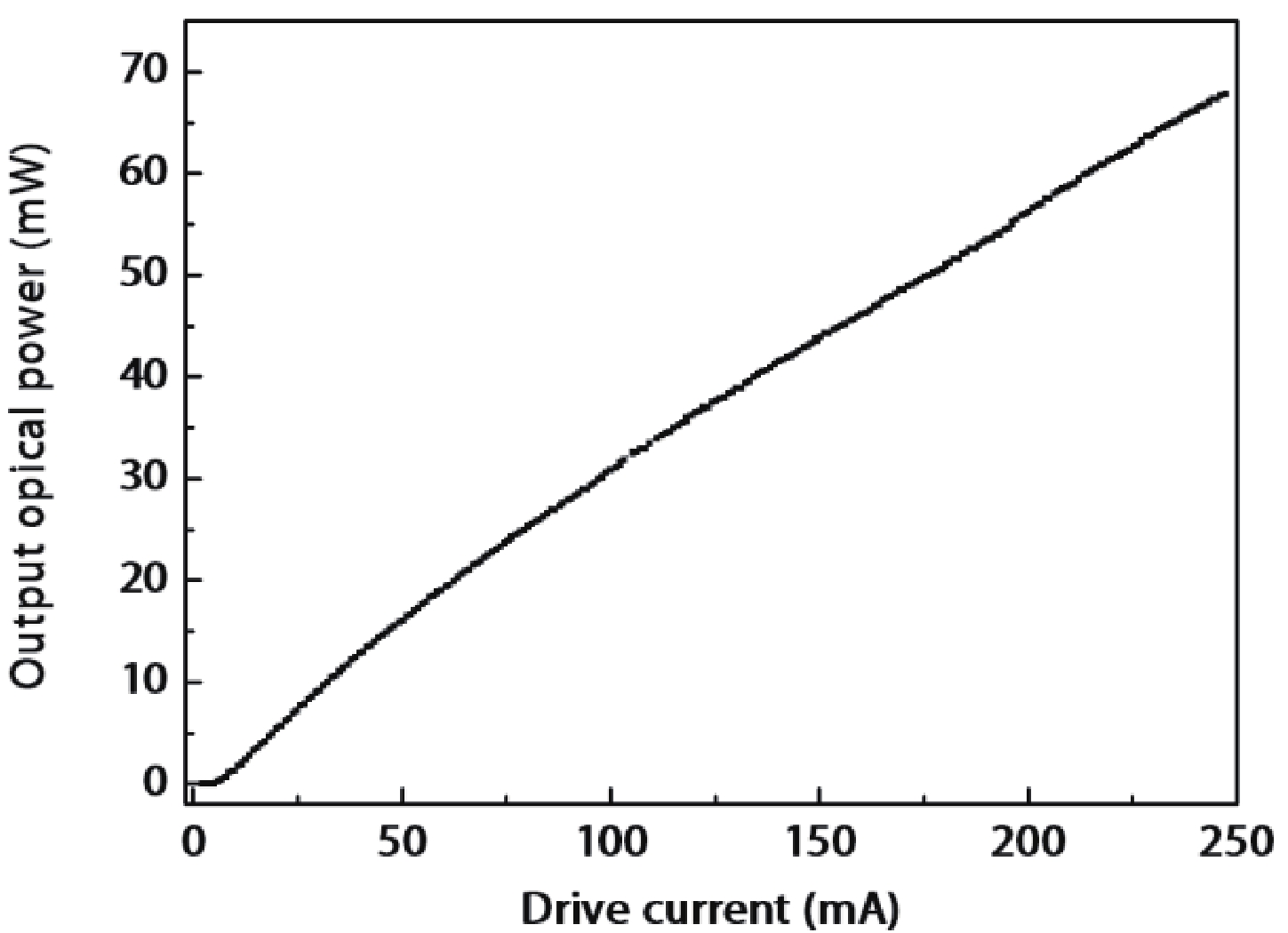
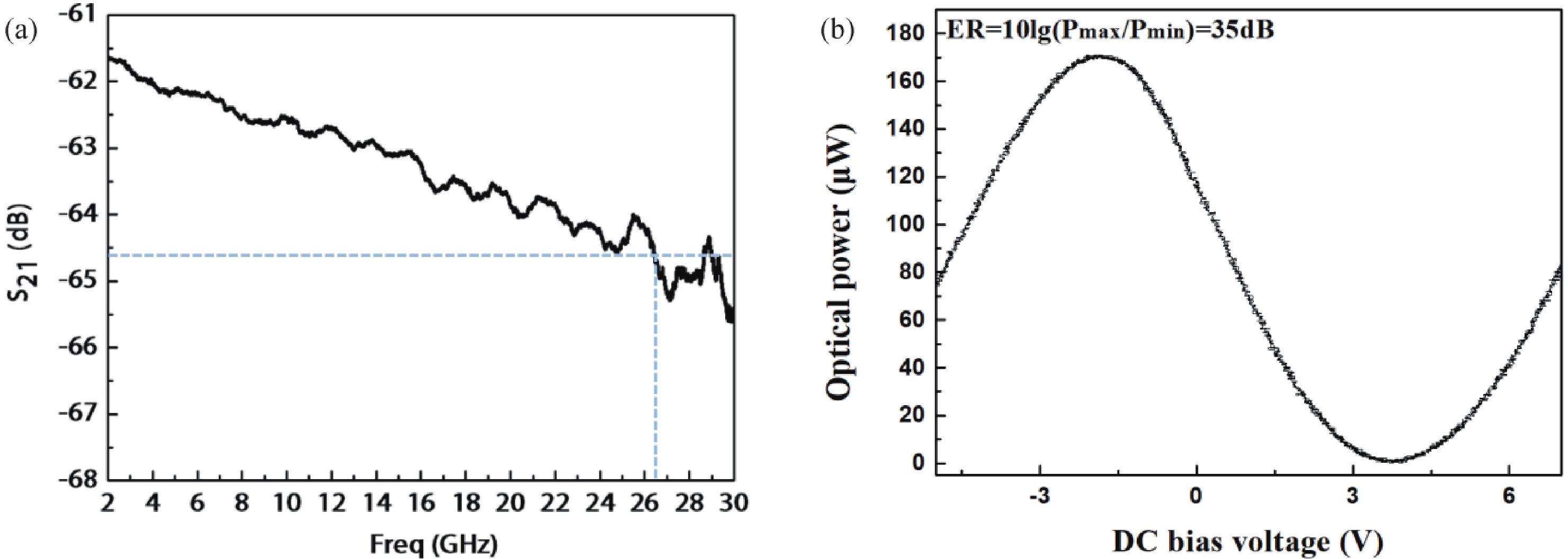
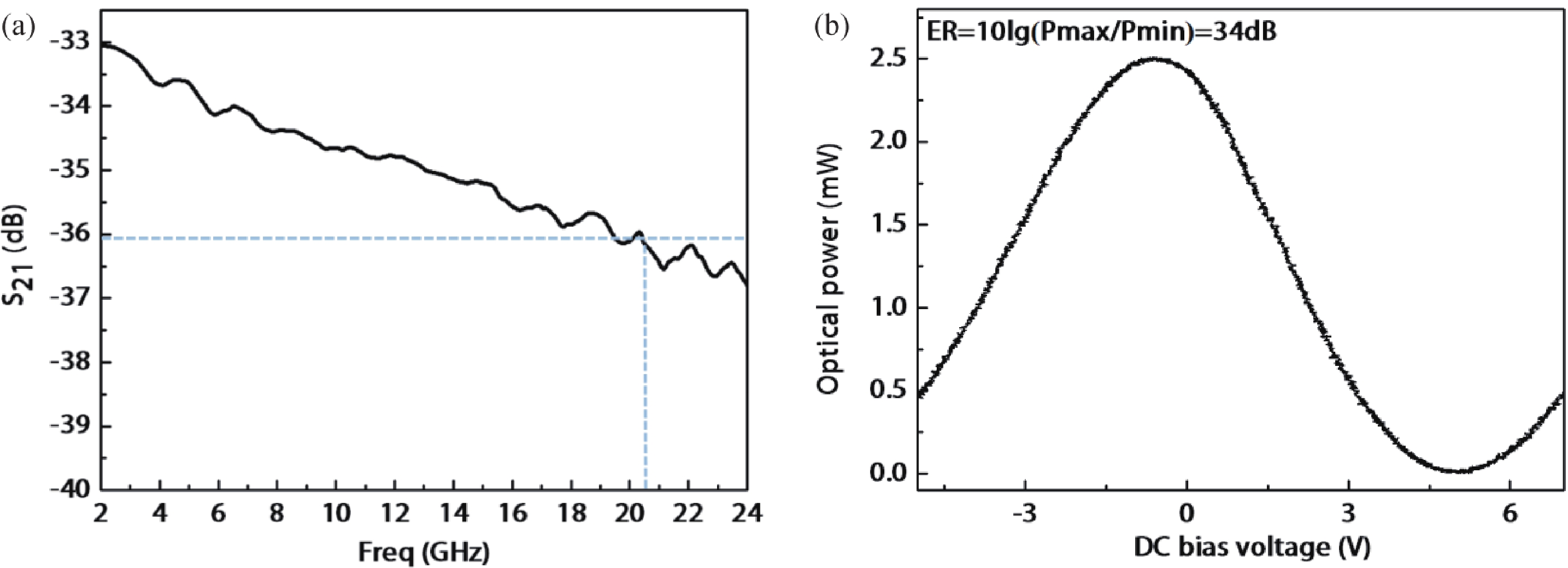
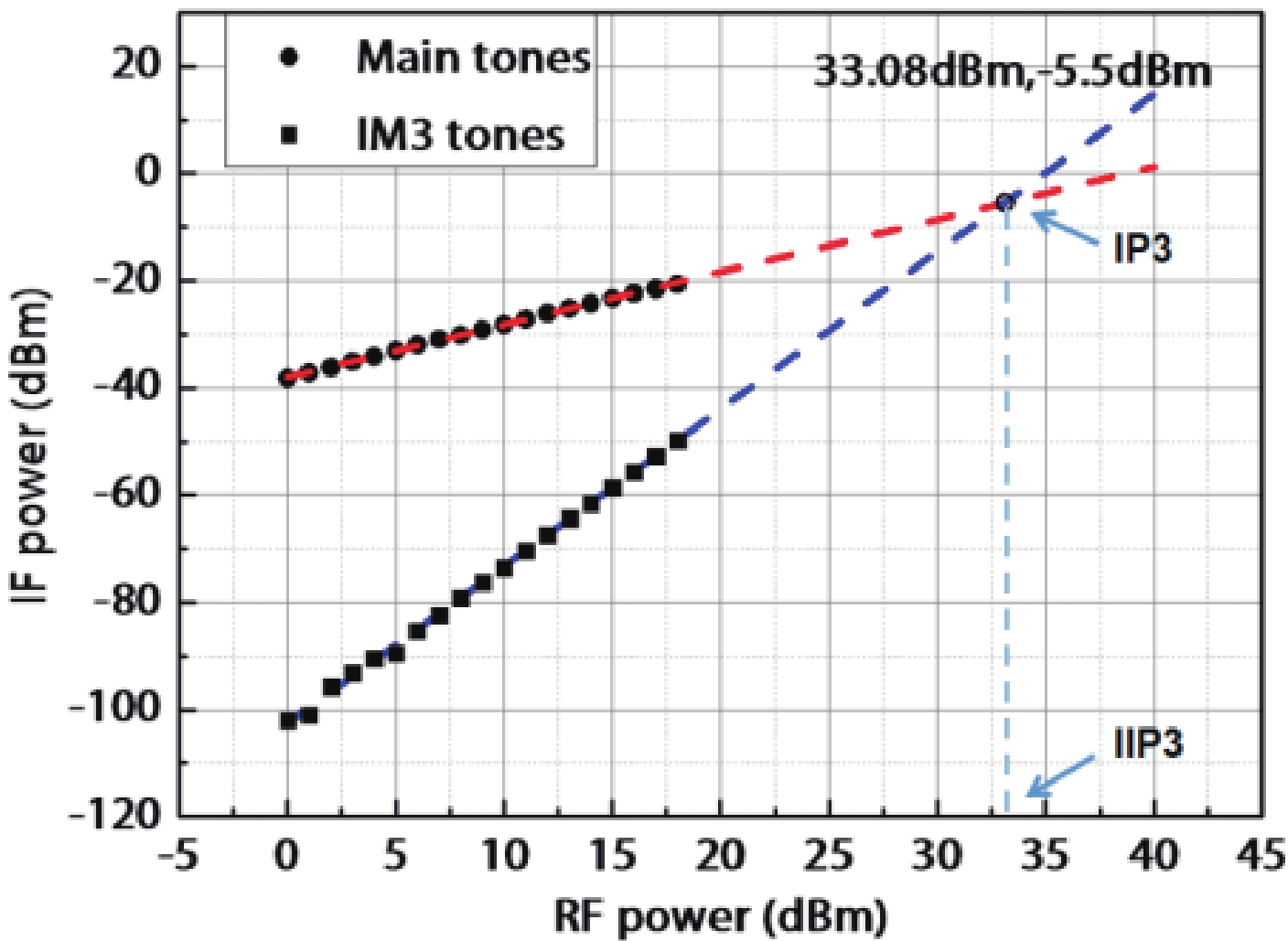
In this work, a hybrid integrated optical transmitter module was designed and fabricated. A proton-exchanged Mach–Zehnder lithium niobate (LiNbO3) modulator chip was chosen to enhance the output extinction ratio. A fiber was used to adjust the rotation of the polarization direction caused by the optical isolator. The whole optical path structure, including the laser chip, lens, fiber, and modulator chip, was simulated to achieve high optical output efficiency. After a series of process improvements, a module with an output extinction ratio of 34 dB and a bandwidth of 20.5 GHz (from 2 GHz) was obtained. The optical output efficiency of the whole module reached approximately 21%. The link performance of the module was also measured.


J. Semicond.
2022, 43(6): 062801 doi: 10.1088/1674-4926/43/6/062801
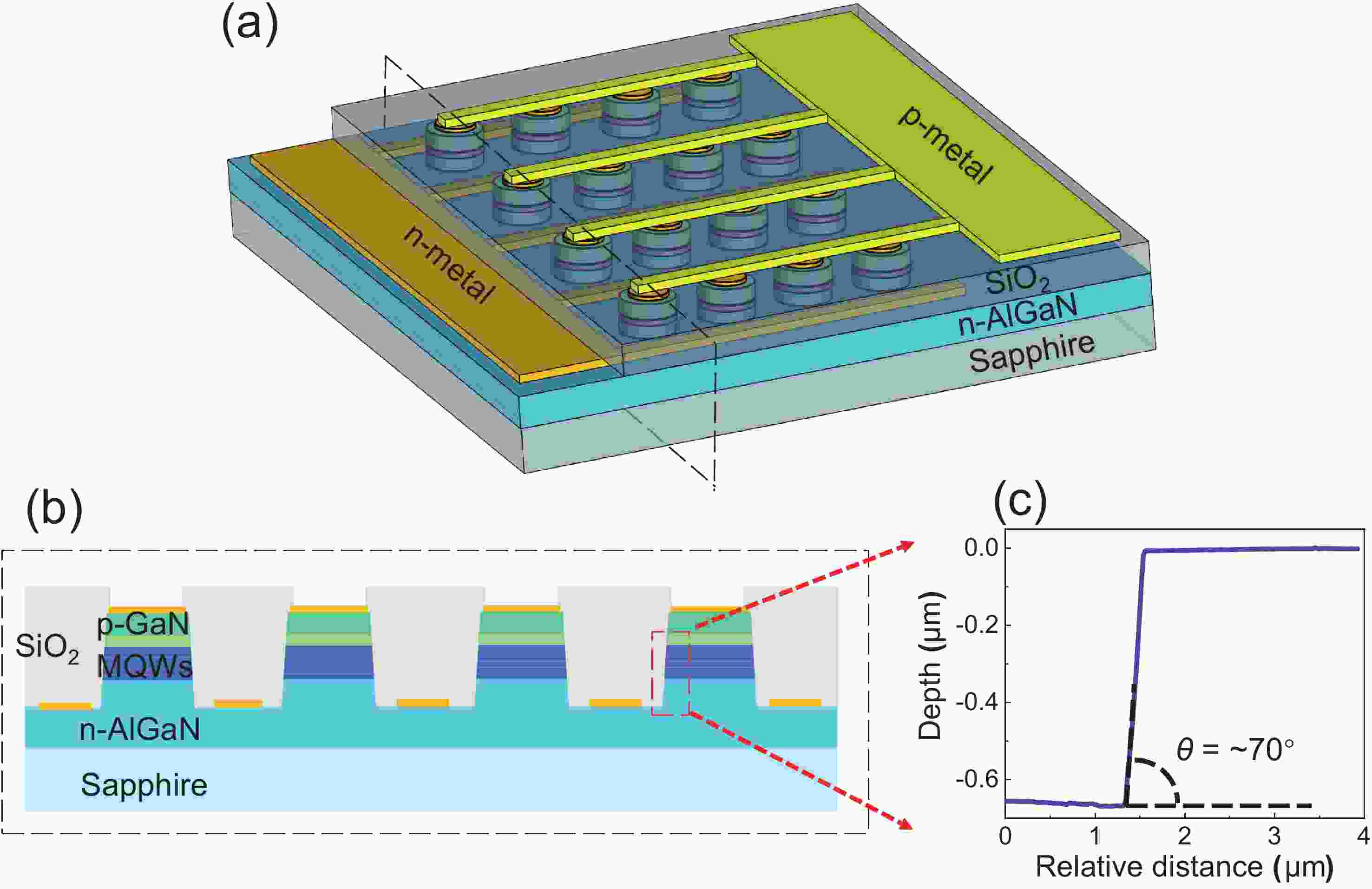
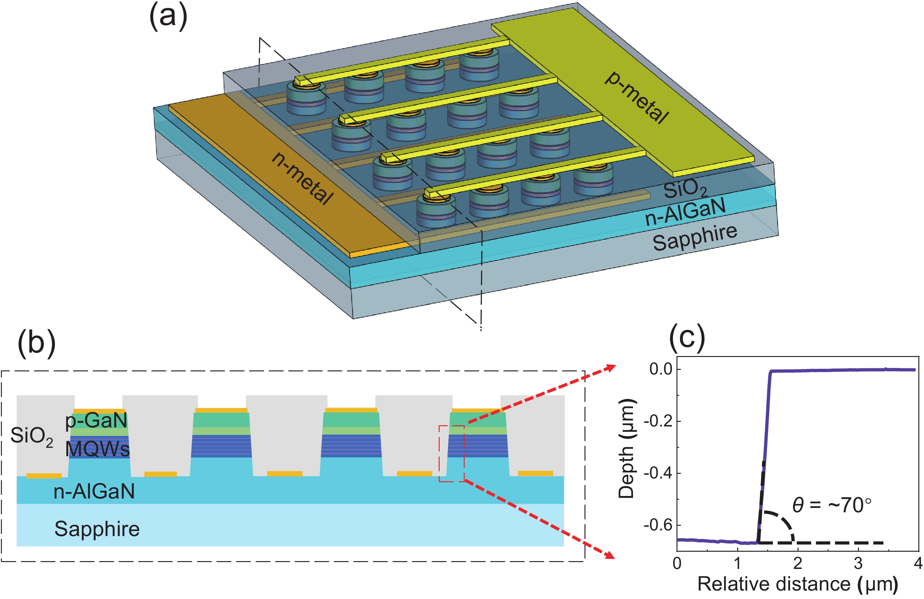
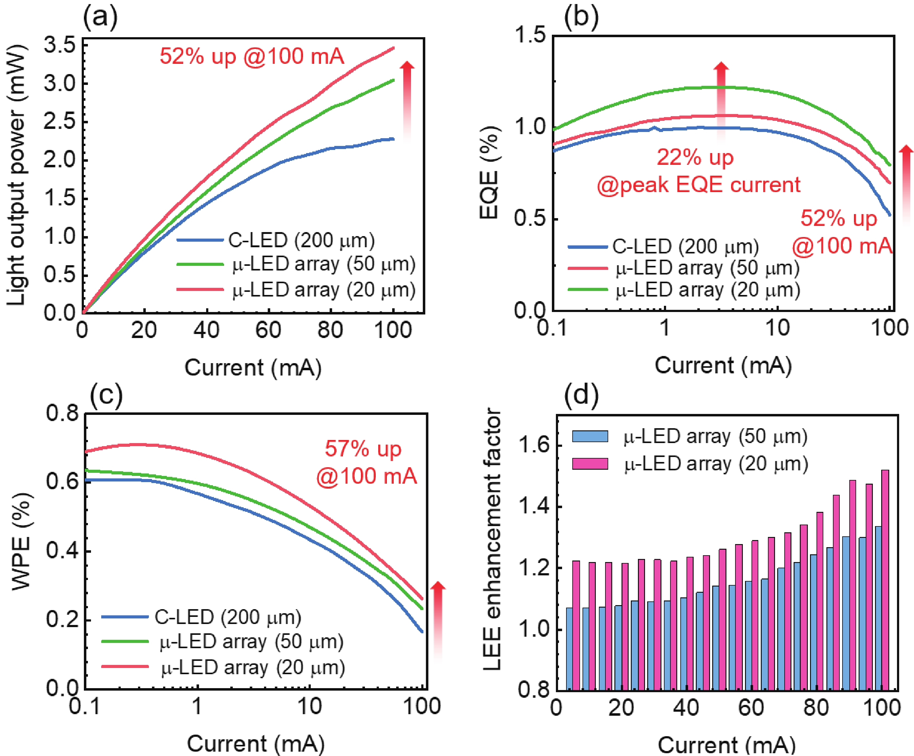
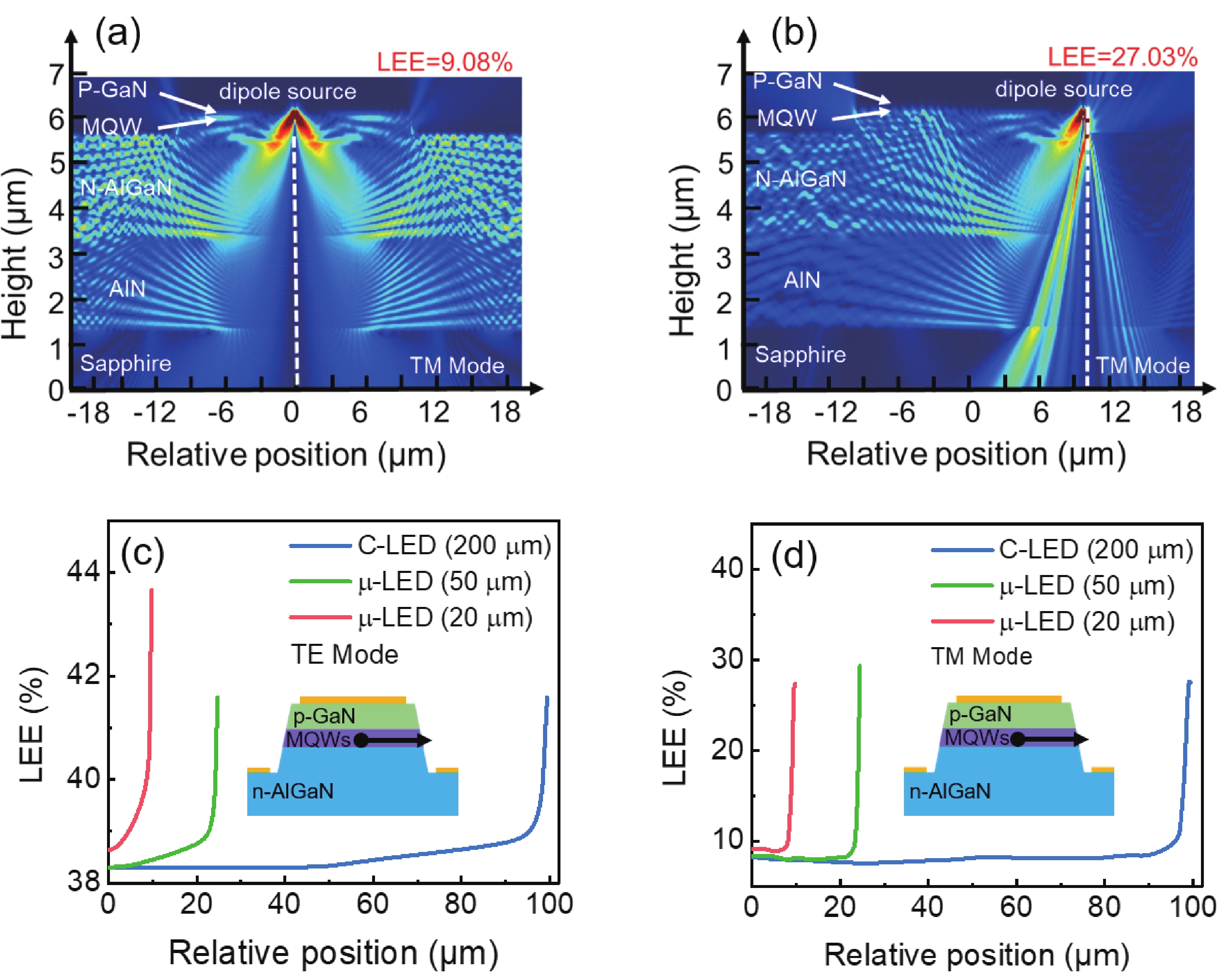
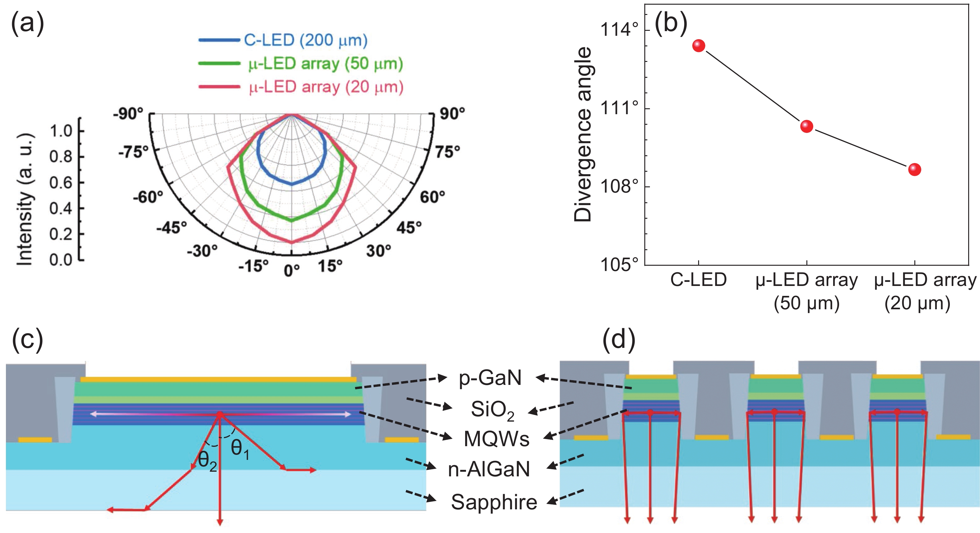
In this work, we design and fabricate a deep ultraviolet (DUV) light-emitting array consisting of 10 × 10 micro-LEDs (μ-LEDs) with each device having 20 μm in diameter. Strikingly, the array demonstrates a significant enhancement of total light output power by nearly 52% at the injection current of 100 mA, in comparison to a conventional large LED chip whose emitting area is the same as the array. A much higher (~22%) peak external quantum efficiency, as well as a smaller efficiency droop for μ-LED array, was also achieved. The numerical calculation reveals that the performance boost can be attributed to the higher light extraction efficiency at the edge of each μ-LED. Additionally, the far-field pattern measurement shows that the μ-LED array possesses a better forward directionality of emission. These findings shed light on the enhancement of the DUV LEDs performance and provide new insights in controlling the light behavior of the μ-LEDs.

J. Semicond.
2022, 43(6): 062802 doi: 10.1088/1674-4926/43/6/062802
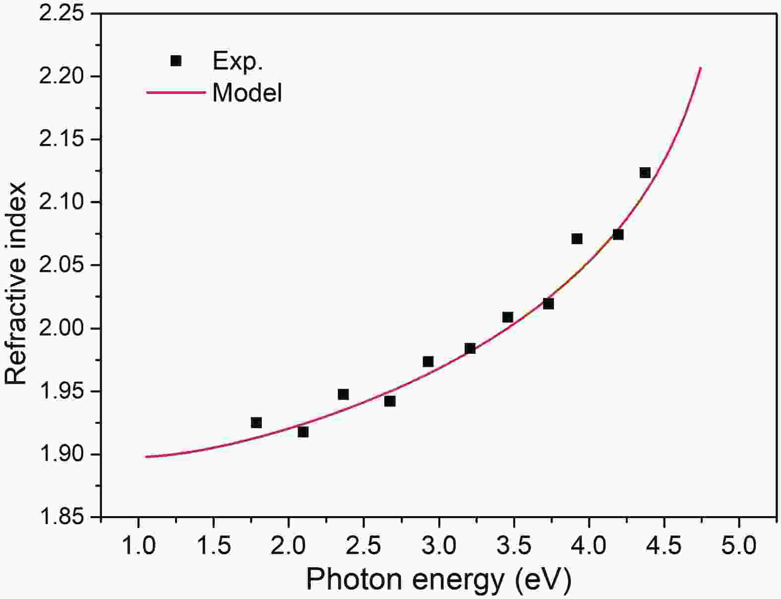
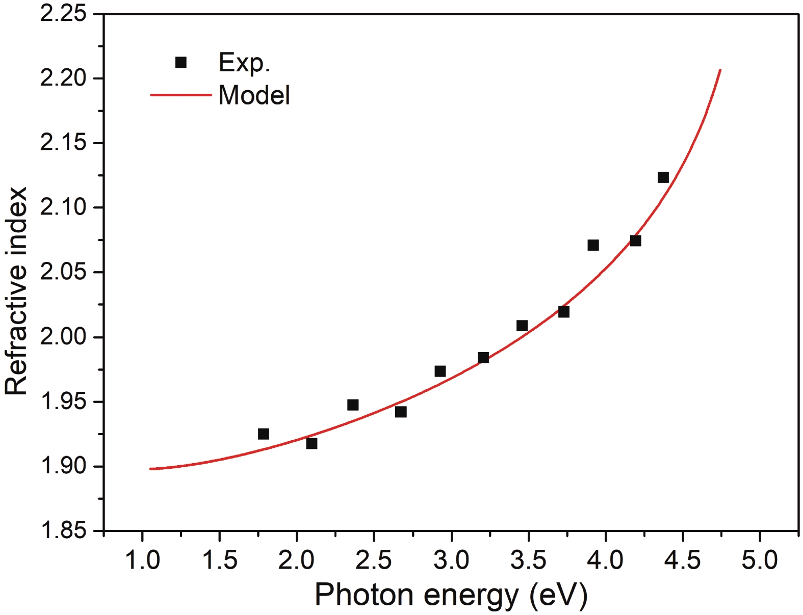
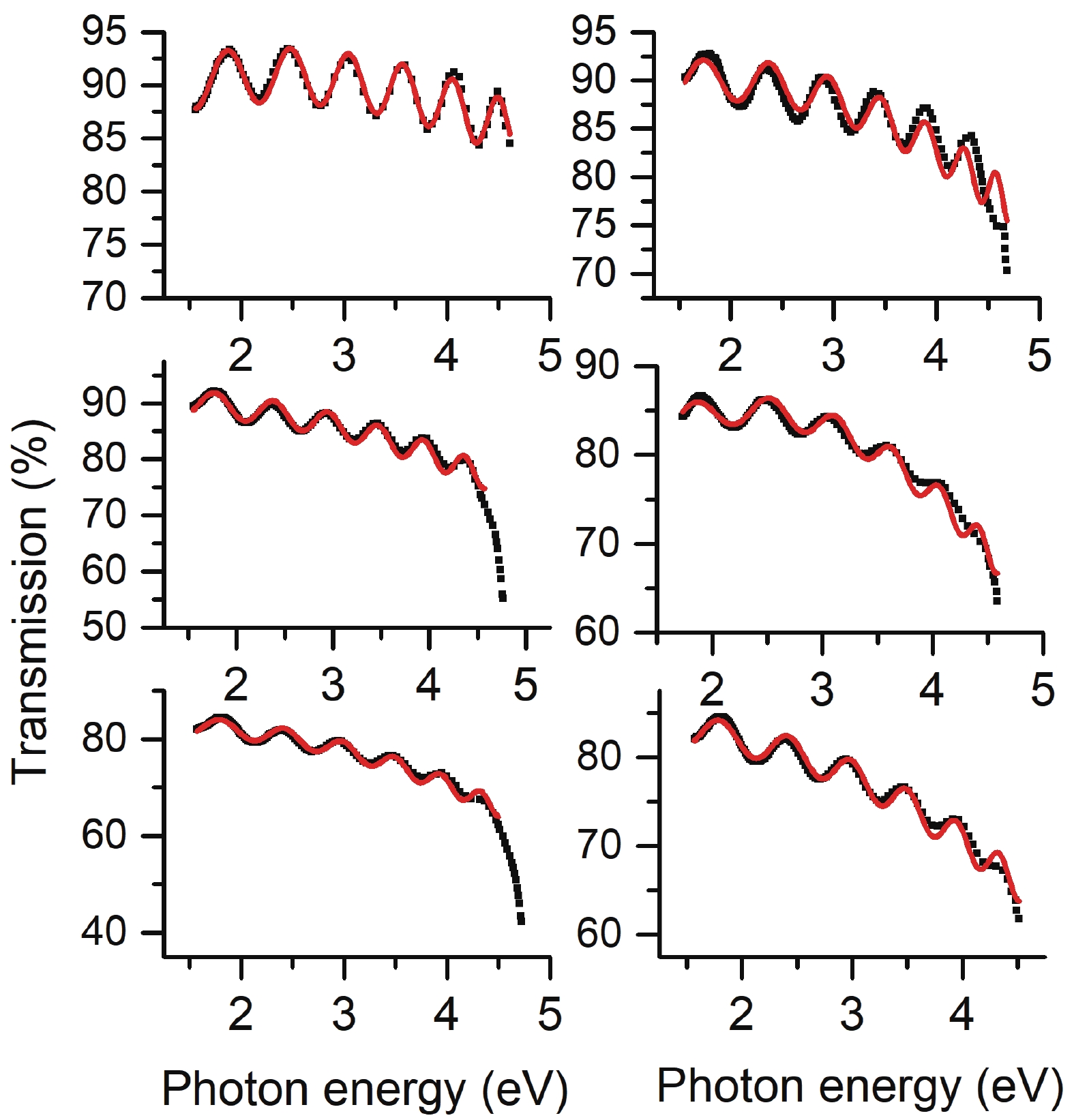
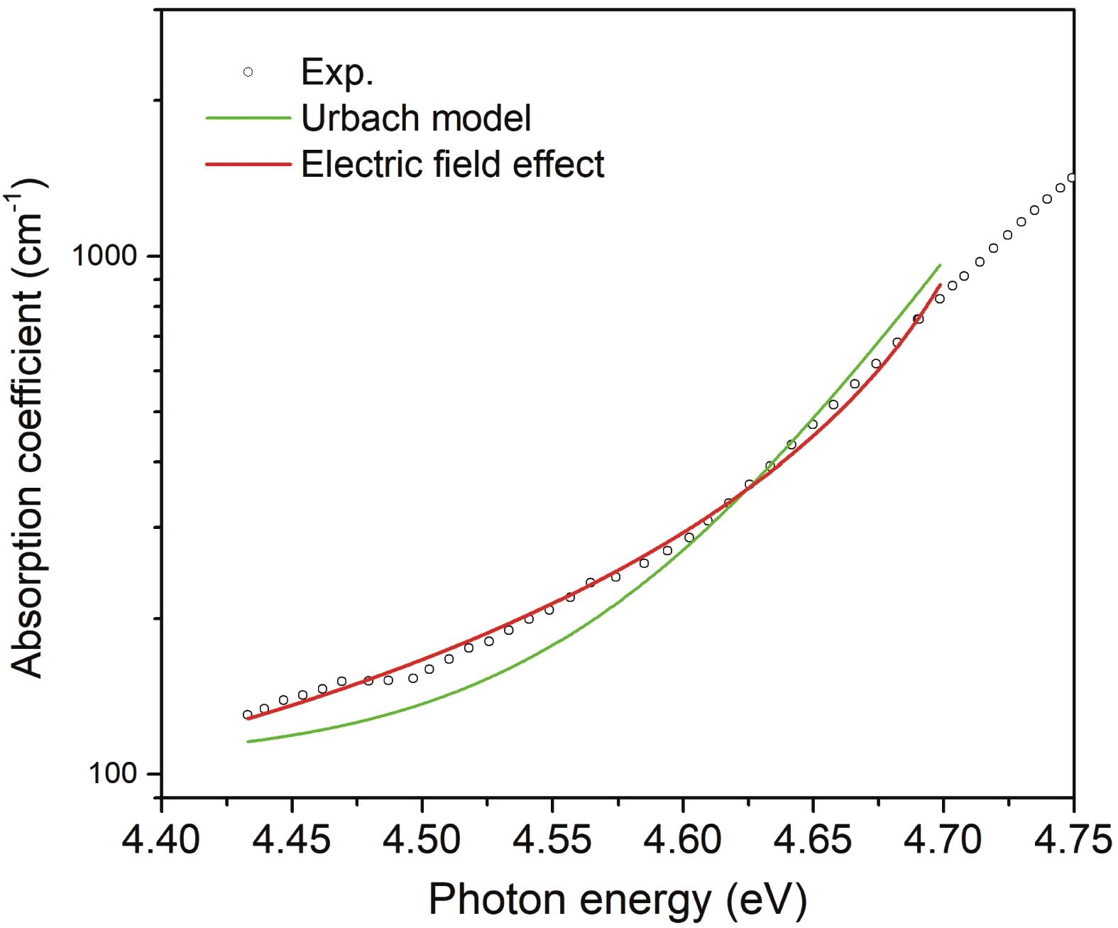
In this article, we present a theoretical study on the sub-bandgap refractive indexes and optical properties of Si-doped β-Ga2O3 thin films based on newly developed models. The measured sub-bandgap refractive indexes of β-Ga2O3 thin film are explained well with the new model, leading to the determination of an explicit analytical dispersion of refractive indexes for photon energy below an effective optical bandgap energy of 4.952 eV for the β-Ga2O3 thin film. Then, the oscillatory structures in long wavelength regions in experimental transmission spectra of Si-doped β-Ga2O3 thin films with different Si doping concentrations are quantitively interpreted utilizing the determined sub-bandgap refractive index dispersion. Meanwhile, effective optical bandgap values of Si-doped β-Ga2O3 thin films are further determined and are found to decrease with increasing the Si doping concentration as expectedly. In addition, the sub-bandgap absorption coefficients of Si-doped β-Ga2O3 thin film are calculated under the frame of the Franz–Keldysh mechanism due to the electric field effect of ionized Si impurities. The theoretical absorption coefficients agree with the available experimental data. These key parameters obtained in the present study may enrich the present understanding of the sub-bandgap refractive indexes and optical properties of impurity-doped β-Ga2O3 thin films.
J. Semicond.
2022, 43(6): 062803 doi: 10.1088/1674-4926/43/6/062803
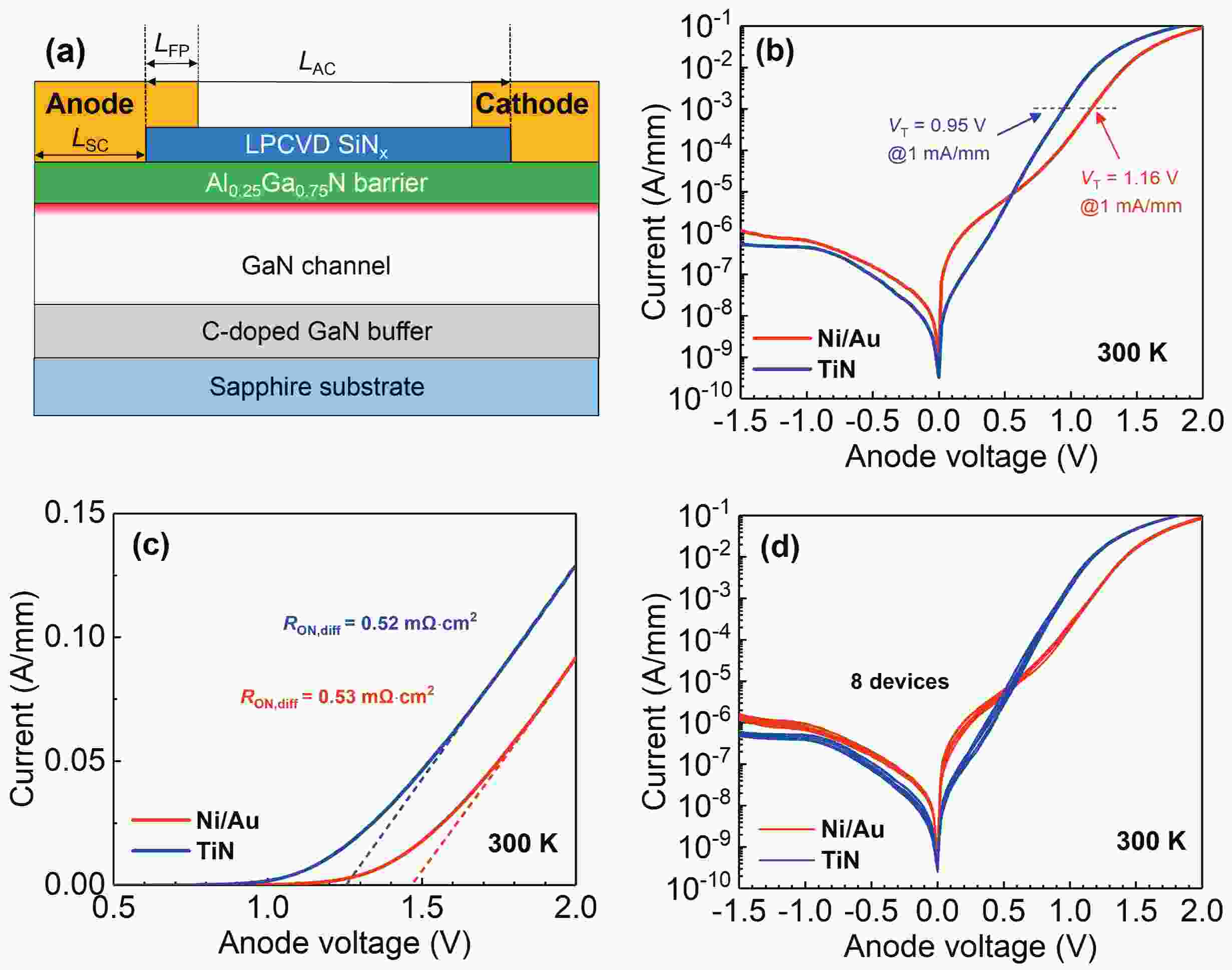
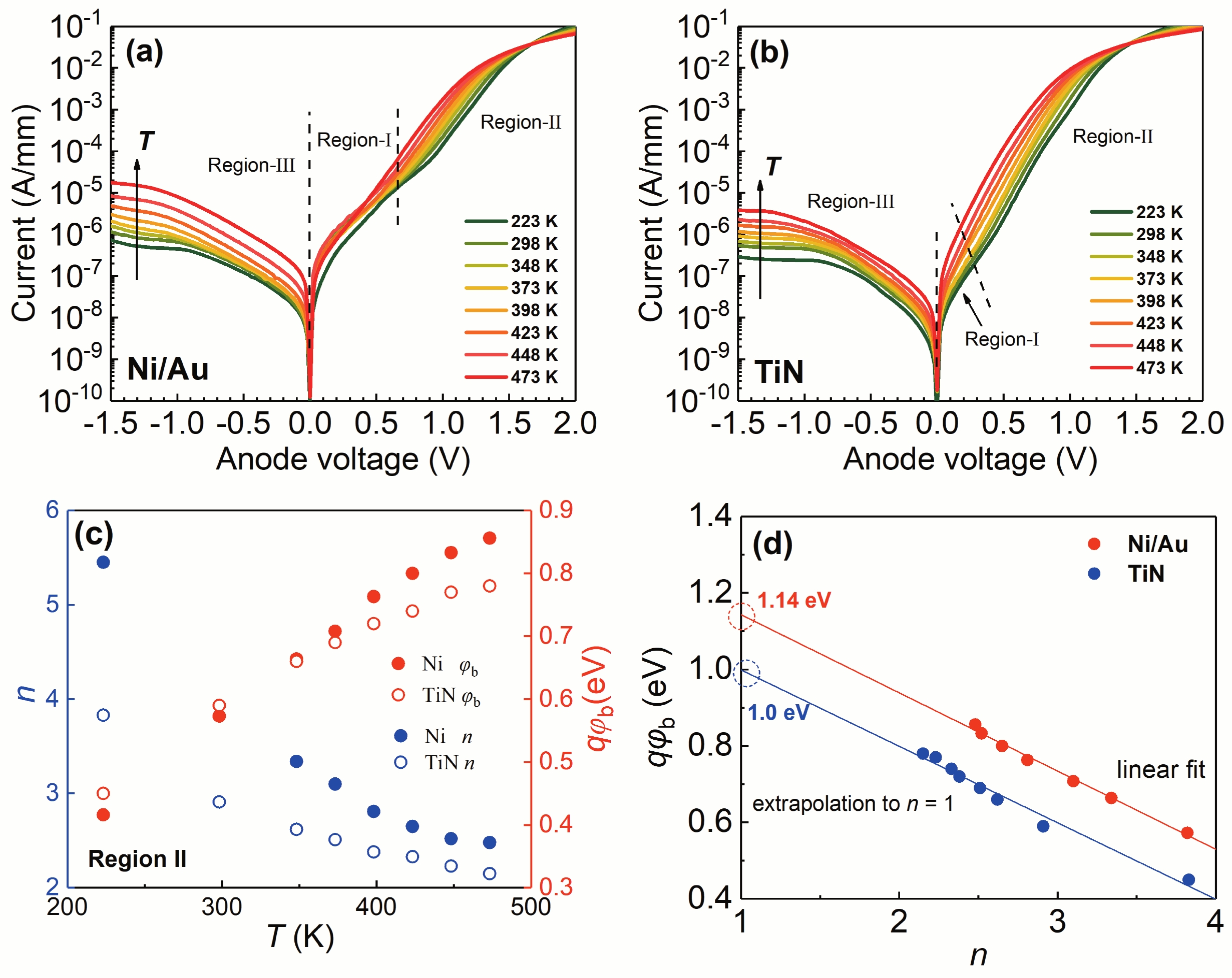
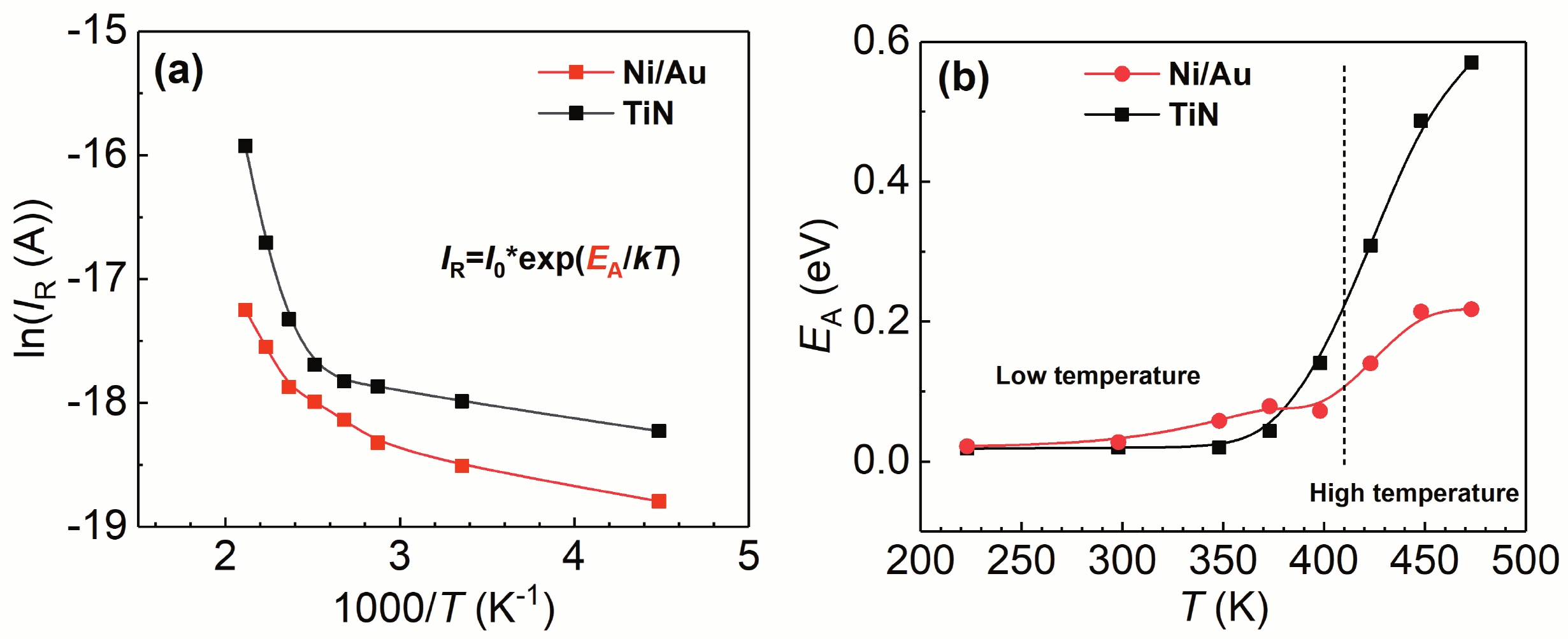
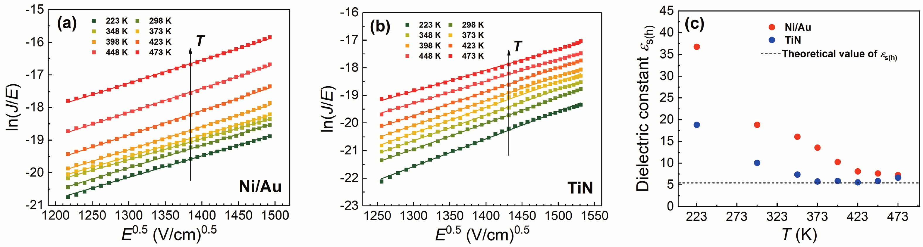
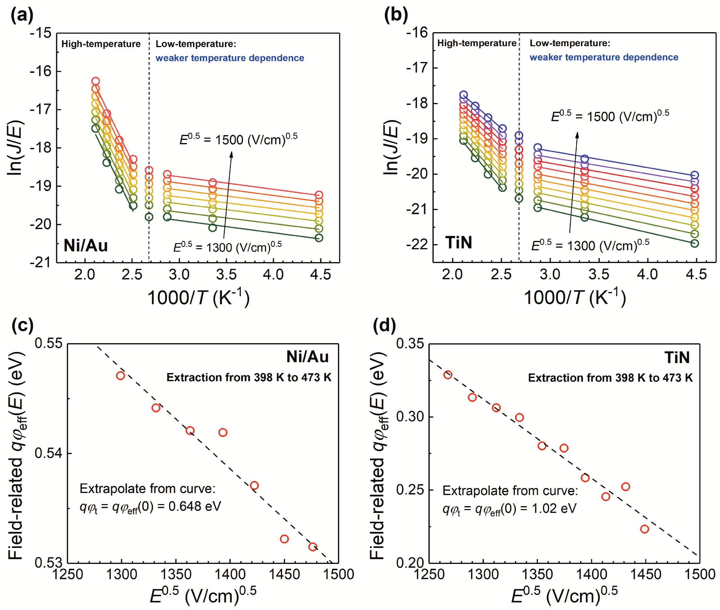
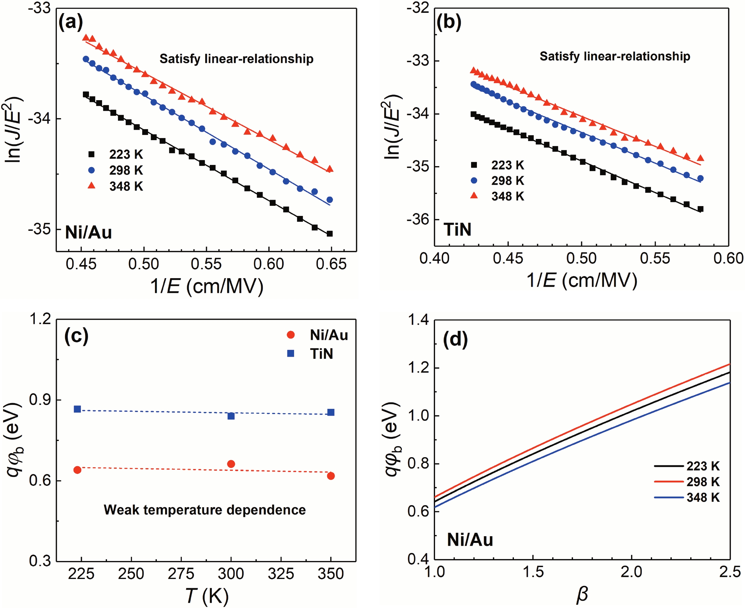
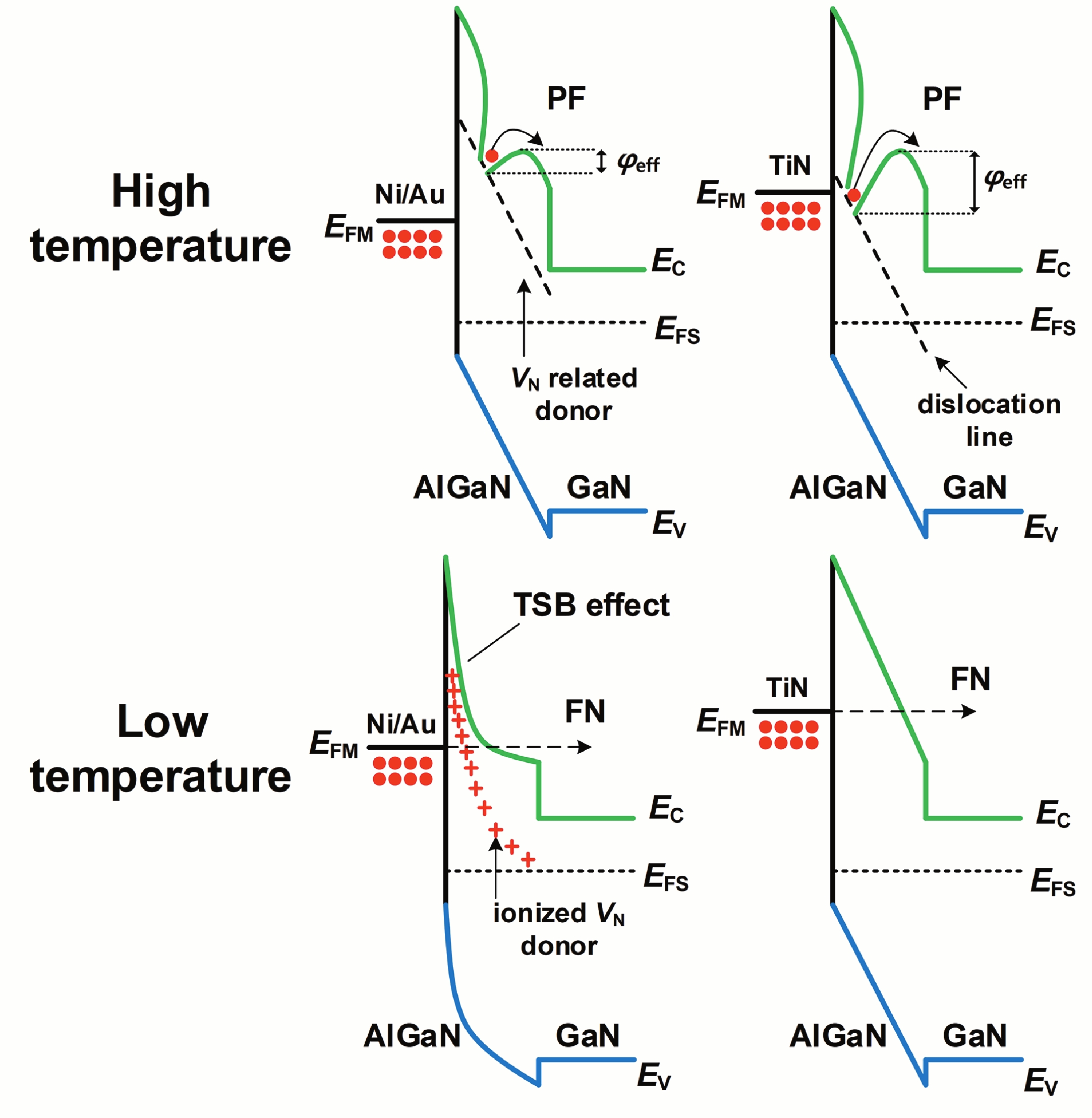
In this work, the optimization of reverse leakage current (IR) and turn-on voltage (VT) in recess-free AlGaN/GaN Schottky barrier diodes (SBDs) was achieved by substituting the Ni/Au anode with TiN anode. To explain this phenomenon, the current transport mechanism was investigated by temperature-dependent current–voltage (I–V) characteristics. For forward bias, the current is dominated by the thermionic emission (TE) mechanisms for both devices. Besides, the presence of inhomogeneity of the Schottky barrier height (qφb) is proved by the linear relationship between qφb and ideality factor. For reverse bias, the current is dominated by two different mechanisms at high temperature and low temperature, respectively. At high temperatures, the Poole–Frenkel emission (PFE) induced by nitrogen-vacancy (VN) is responsible for the high IR in Ni/Au anode. For TiN anode, the IR is dominated by the PFE from threading dislocation (TD), which can be attributed to the decrease of VN due to the suppression of N diffusion at the interface of Schottky contact. At low temperatures, the IR of both diodes is dominated by Fowler–Nordheim (FN) tunneling. However, the VN donor enhances the electric field in the barrier layer, thus causing a higher IR in Ni/Au anode than TiN anode, as confirmed by the modified FN model.


J. Semicond.
2022, 43(6): 062804 doi: 10.1088/1674-4926/43/6/062804
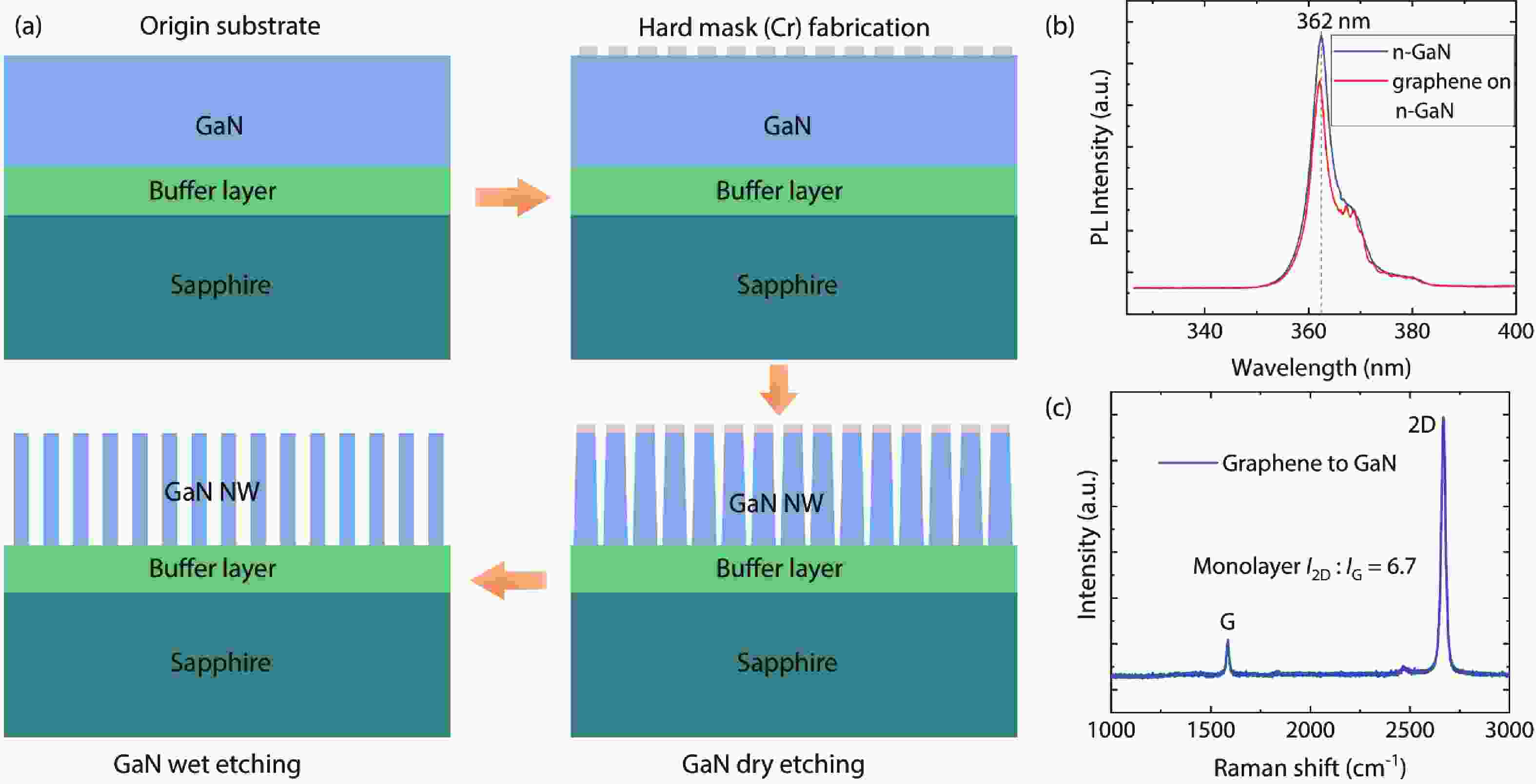
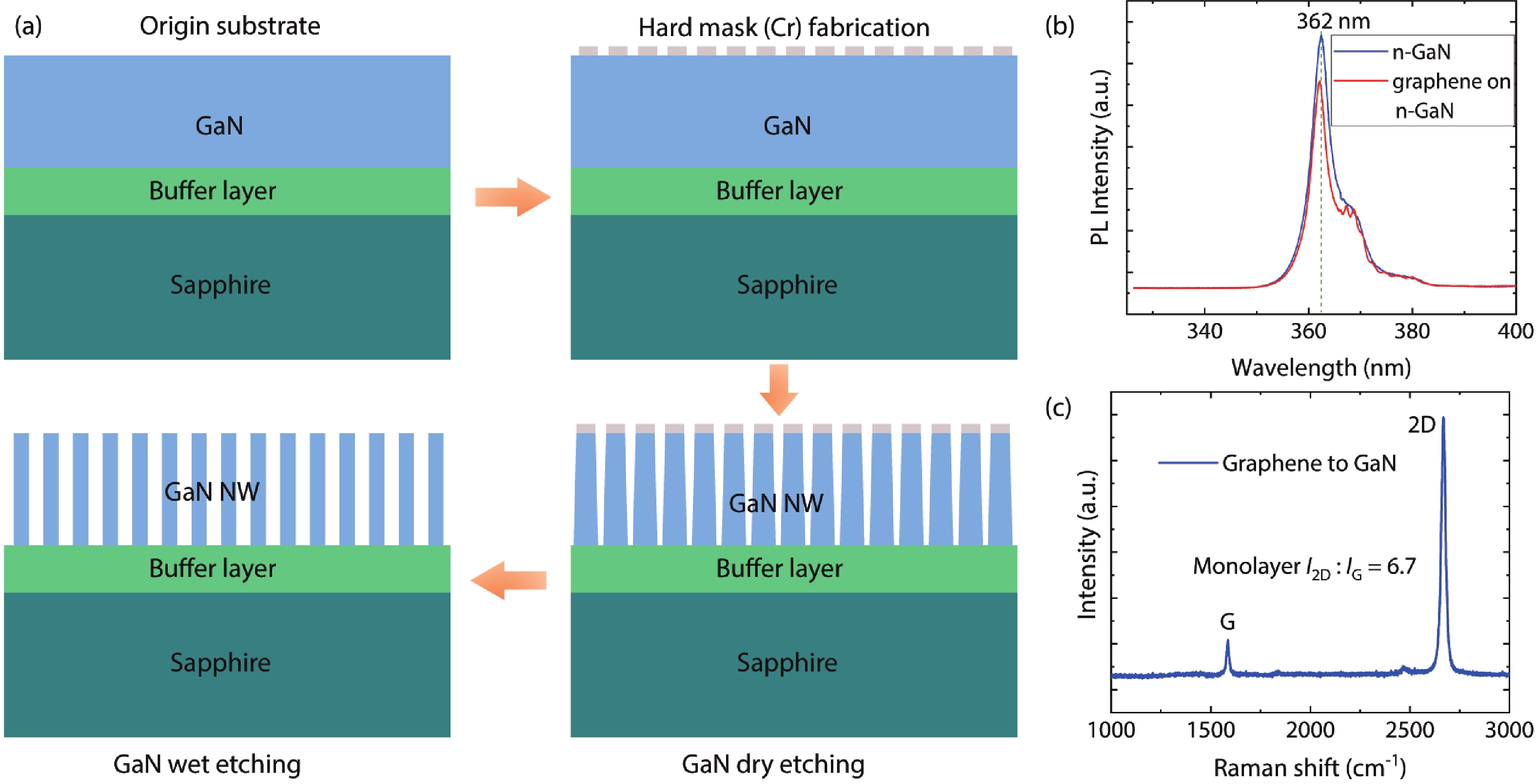
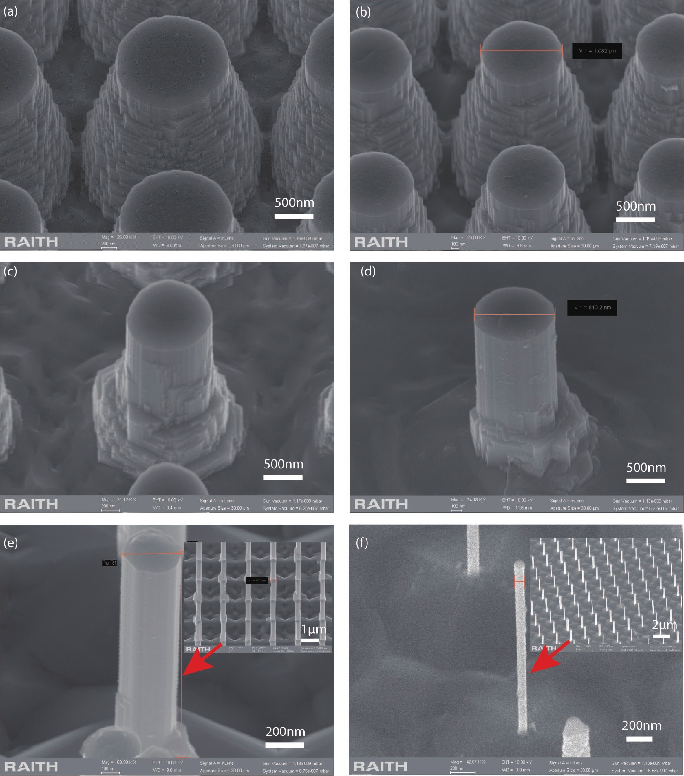
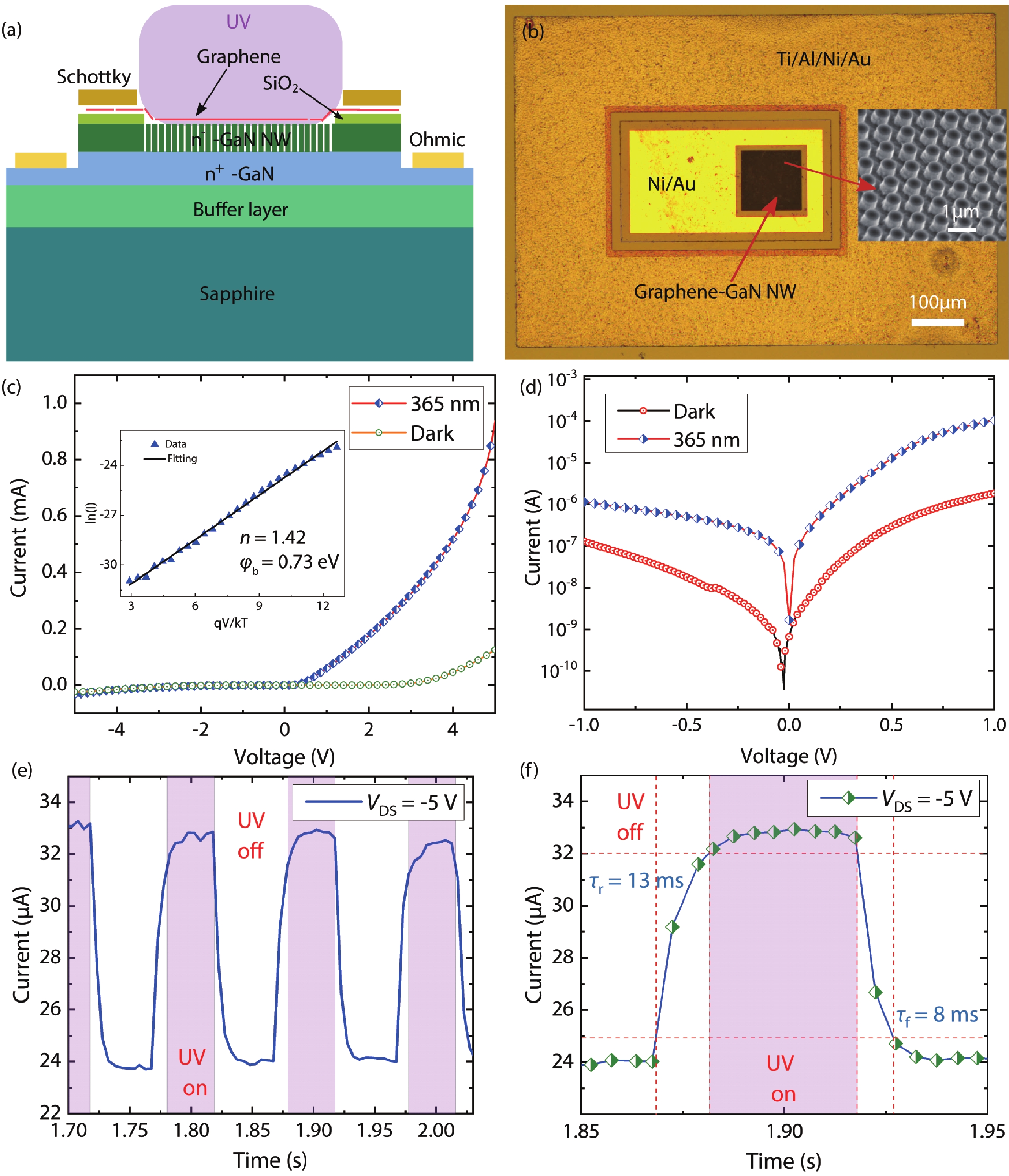
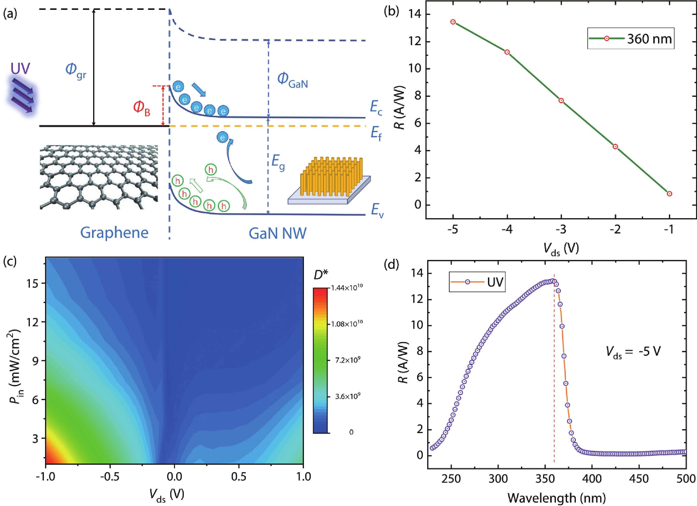
GaN has been widely used in the fabrication of ultraviolet photodetectors because of its outstanding properties. In this paper, we report a graphene–GaN nanorod heterostructure photodetector with fast photoresponse in the UV range. GaN nanorods were fabricated by a combination mode of dry etching and wet etching. Furthermore, a graphene–GaN nanorod heterostructure ultraviolet detector was fabricated and its photoelectric properties were measured. The device exhibits a fast photoresponse in the UV range. The rising time and falling time of the transient response were 13 and 8 ms, respectively. A high photovoltaic responsivity up to 13.9 A/W and external quantum efficiency up to 479% were realized at the UV range. The specific detectivity D* = 1.44 × 10¹⁰ Jones was obtained at –1 V bias in ambient conditions. The spectral response was measured and the highest response was observed at the 360 nm band.
J. Semicond.
2022, 43(6): 062301 doi: 10.1088/1674-4926/43/6/062301
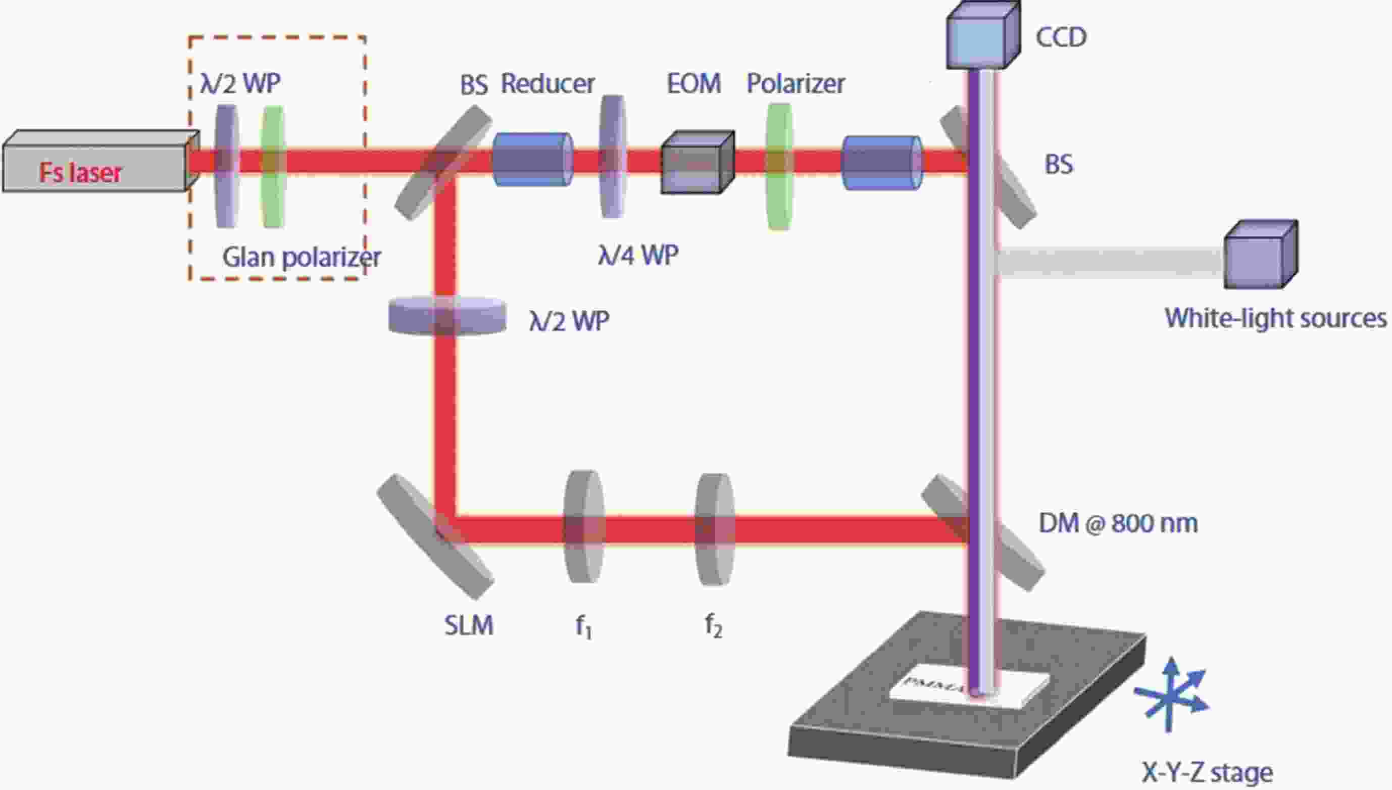
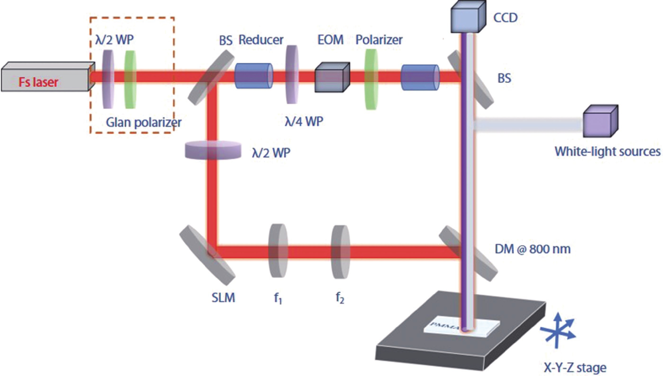
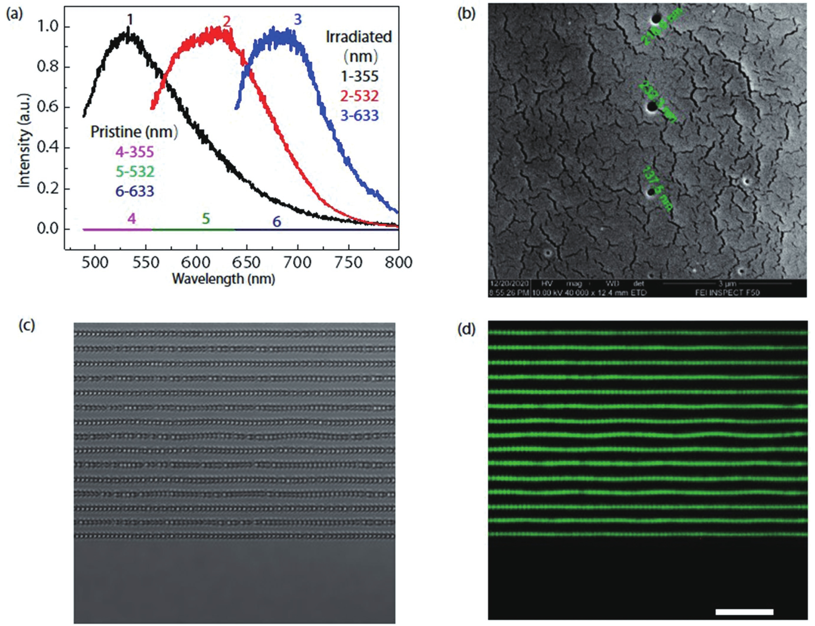
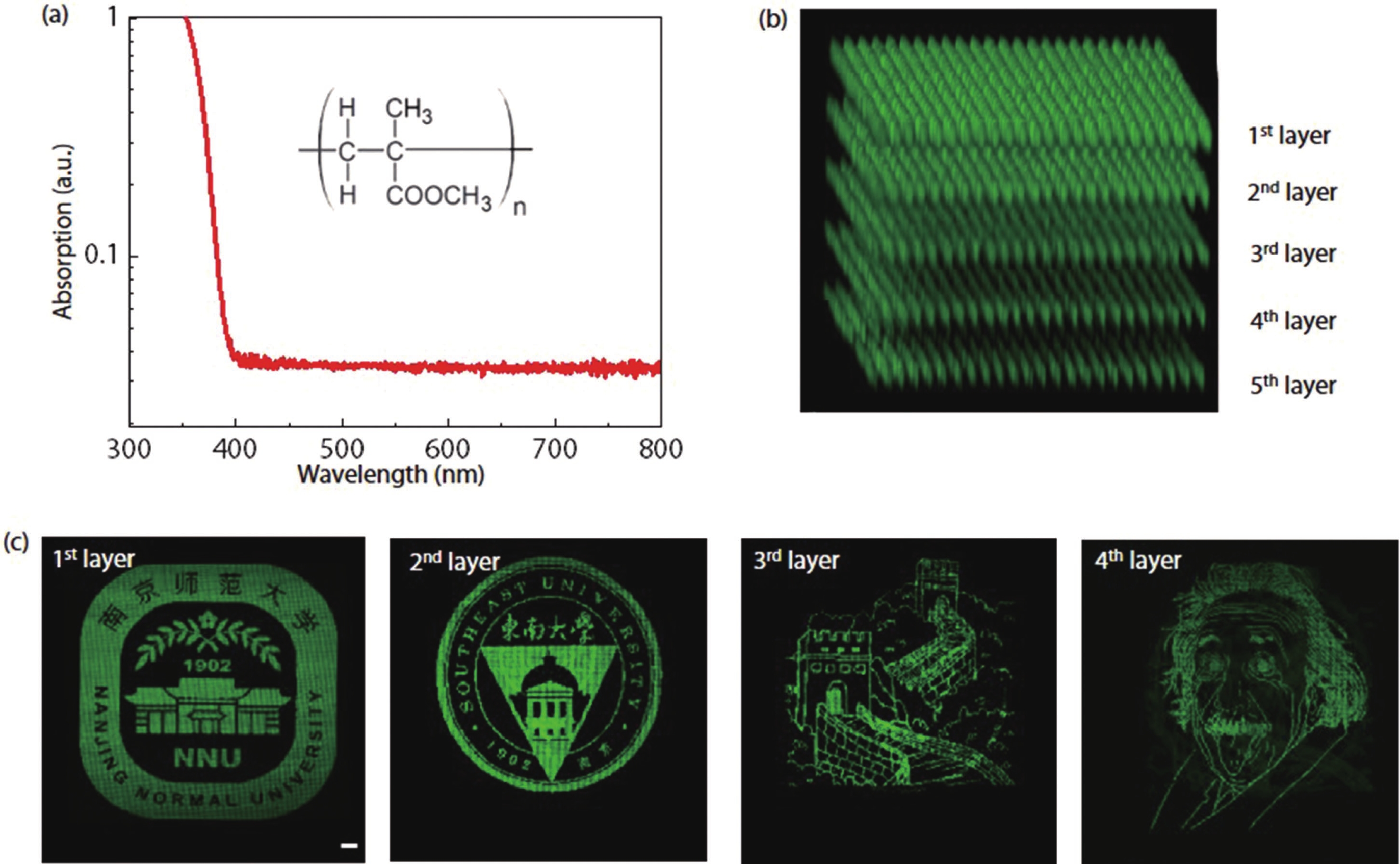
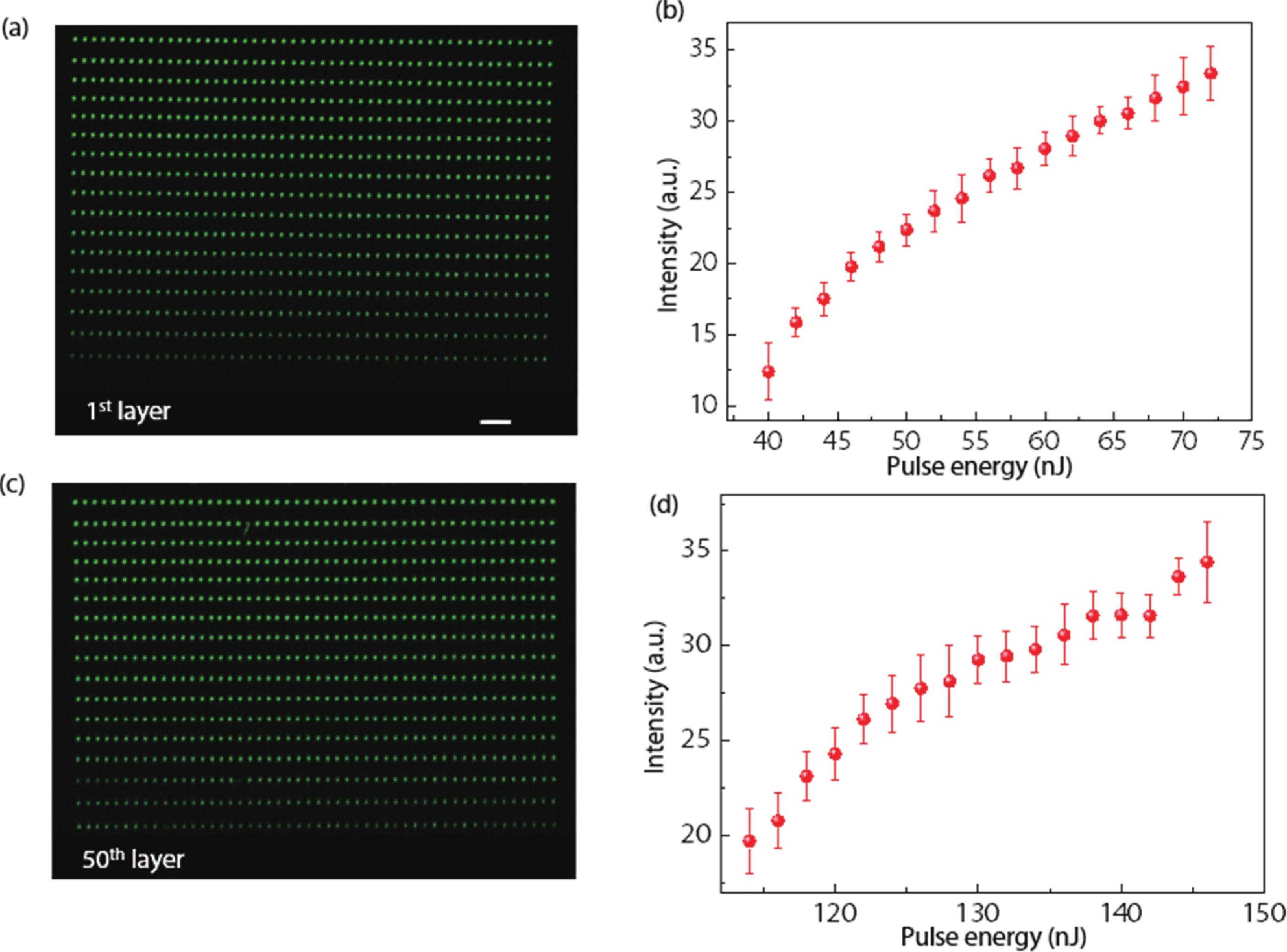
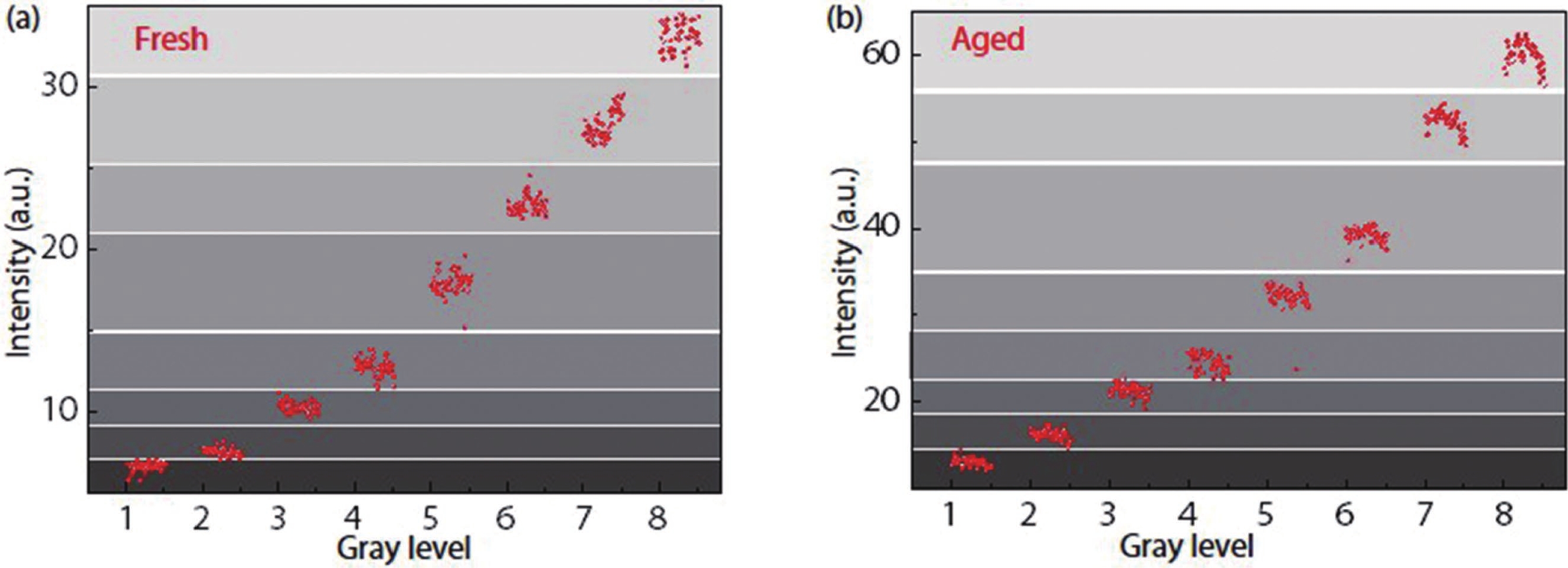
The explosive growth of the global data volume demands new and advanced data storage methods. Here, we report that data storage with ultrahigh capacity (~1 TB per disc) can be realized in low-cost plastics, including polycarbonate (PC), precipitated calcium carbonate (PCC), polystyrene (PS), and polymethyl methacrylate (PMMA), via direct fs laser writing. The focused fs laser can modify the fluorescence of written regions on the surface and in the interior of PMMA, enabling three-dimensional (3D) information storage. Through the 3D laser processing platform, a 50-layer data record with low bit error (0.96%) is archived. Visual reading of data is empowered by the fluorescence contrast. The broad variation of fluorescence intensity assigns 8 gray levels, corresponding to 3 bits on each spot. The gray levels of each layer present high stability after long-term aging cycles, confirming the robustness of data storage. Upon single pulse control via a high-frequency electro-optic modulator (EOM), a fast writing speed (~1 kB/s) is achieved, which is limited by the repetition frequency of the fs laser.