Issue Browser
Volume 44, Issue 11,
Nov 2023
Column


J. Semicond.
2023, 44(11): 111301 doi: 10.1088/1674-4926/44/11/111301

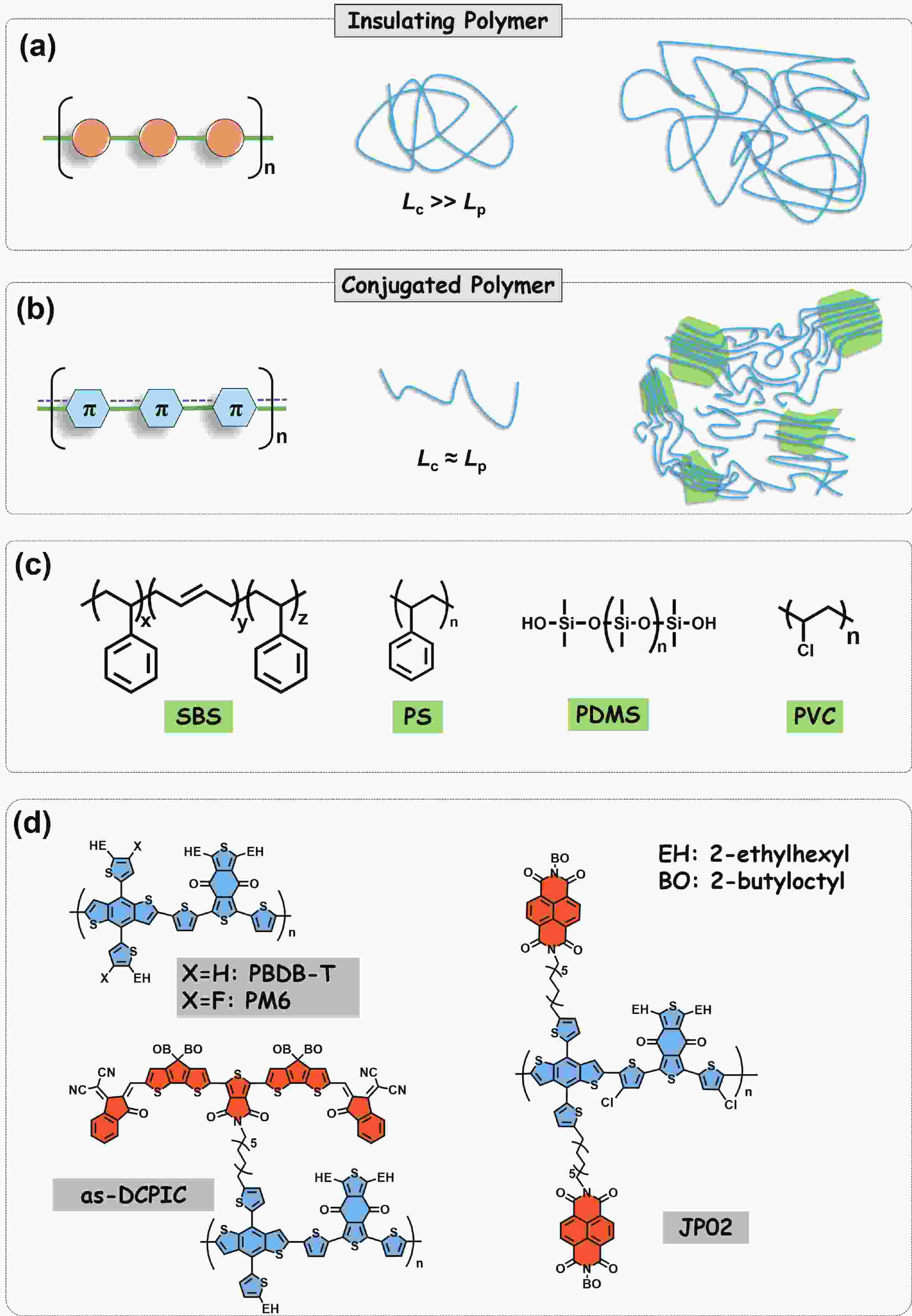
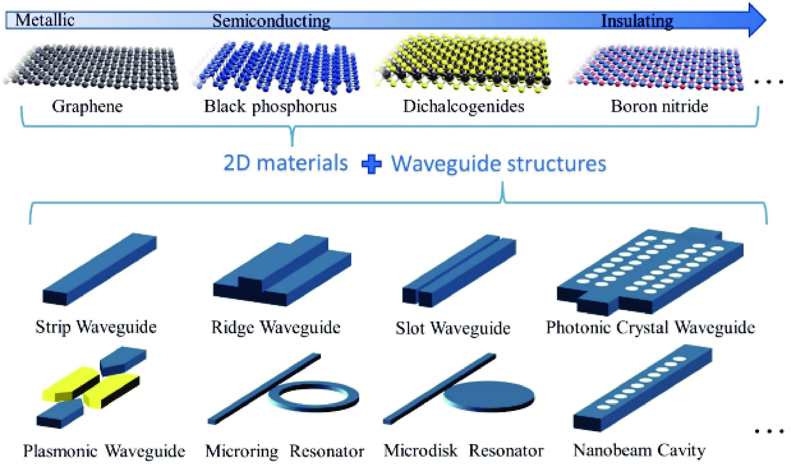
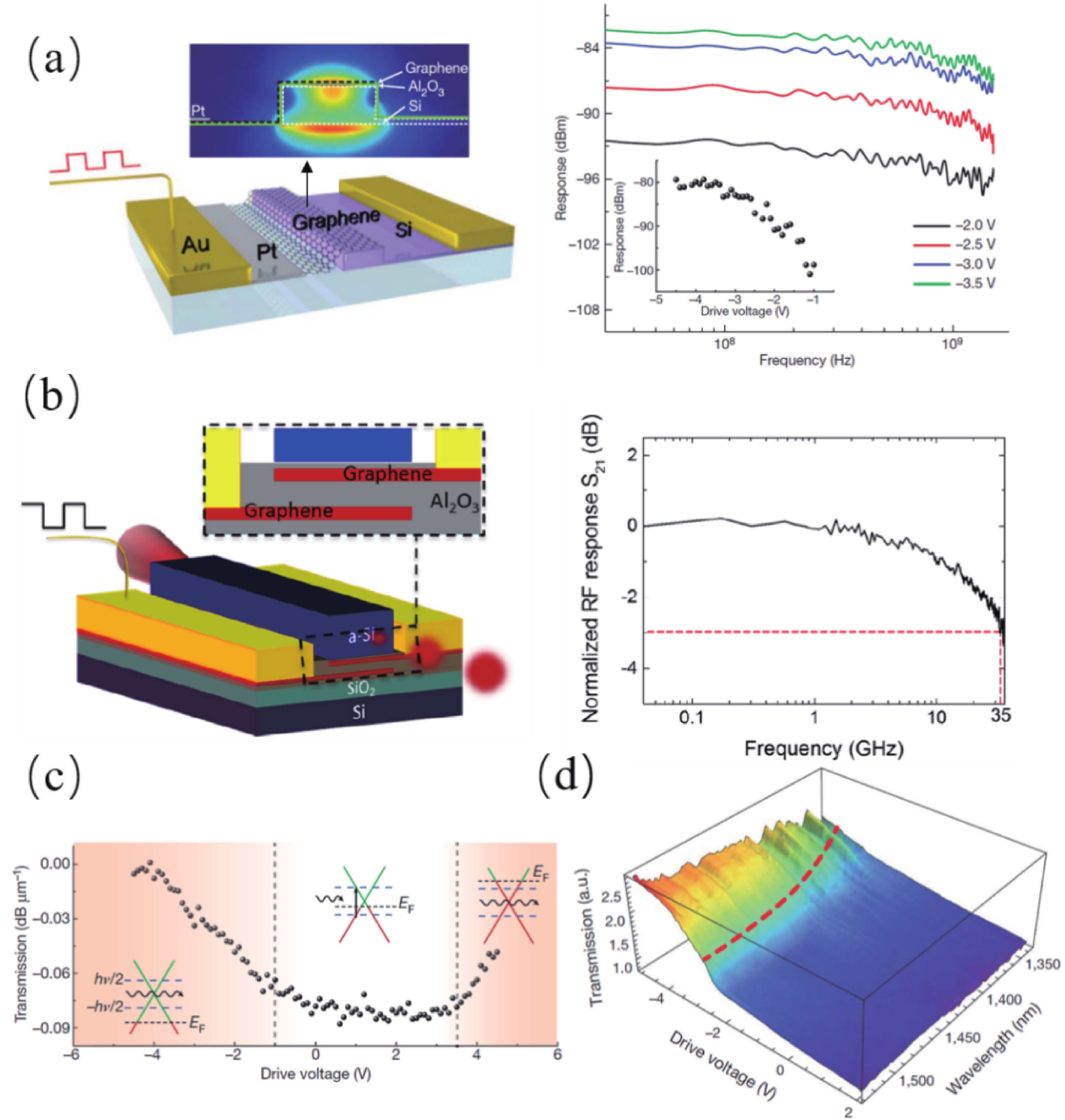
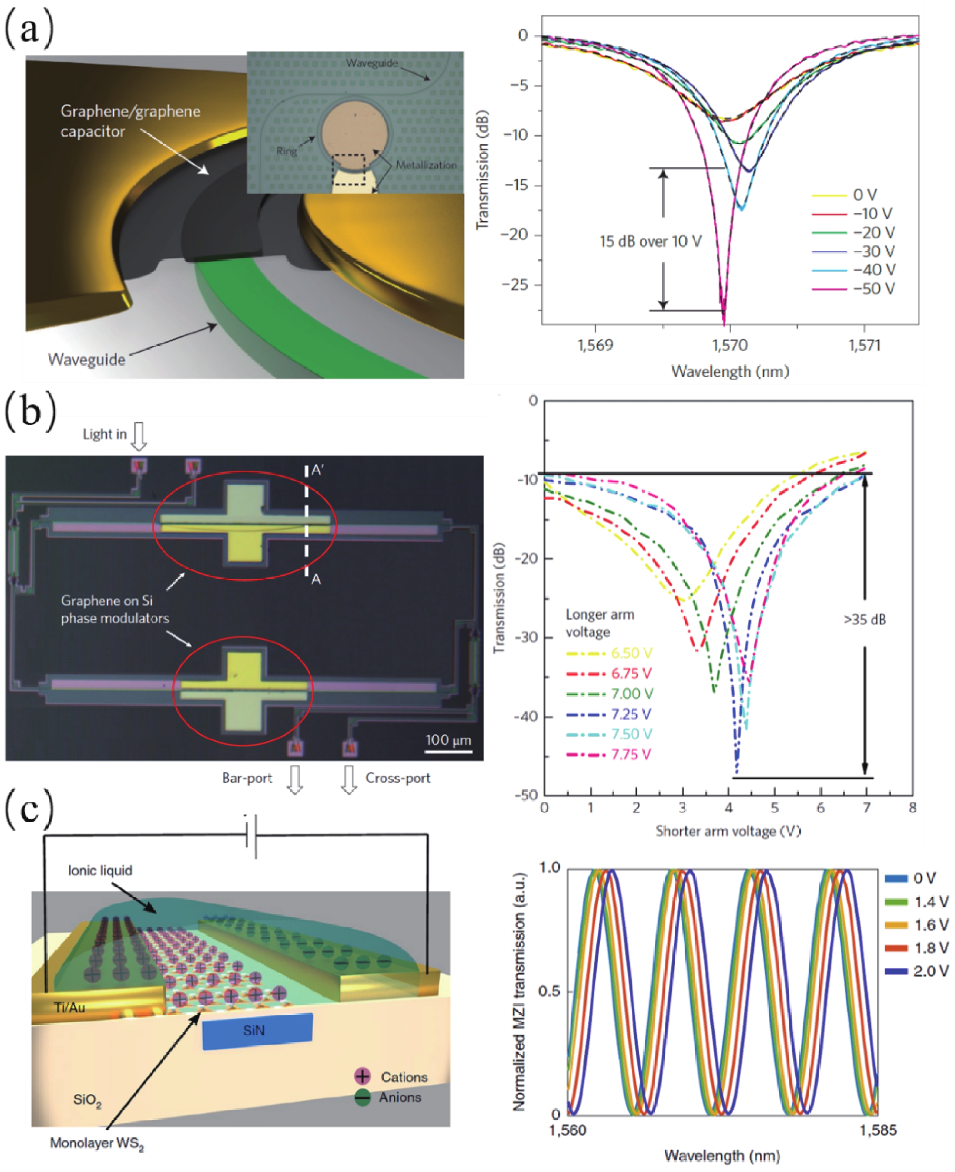
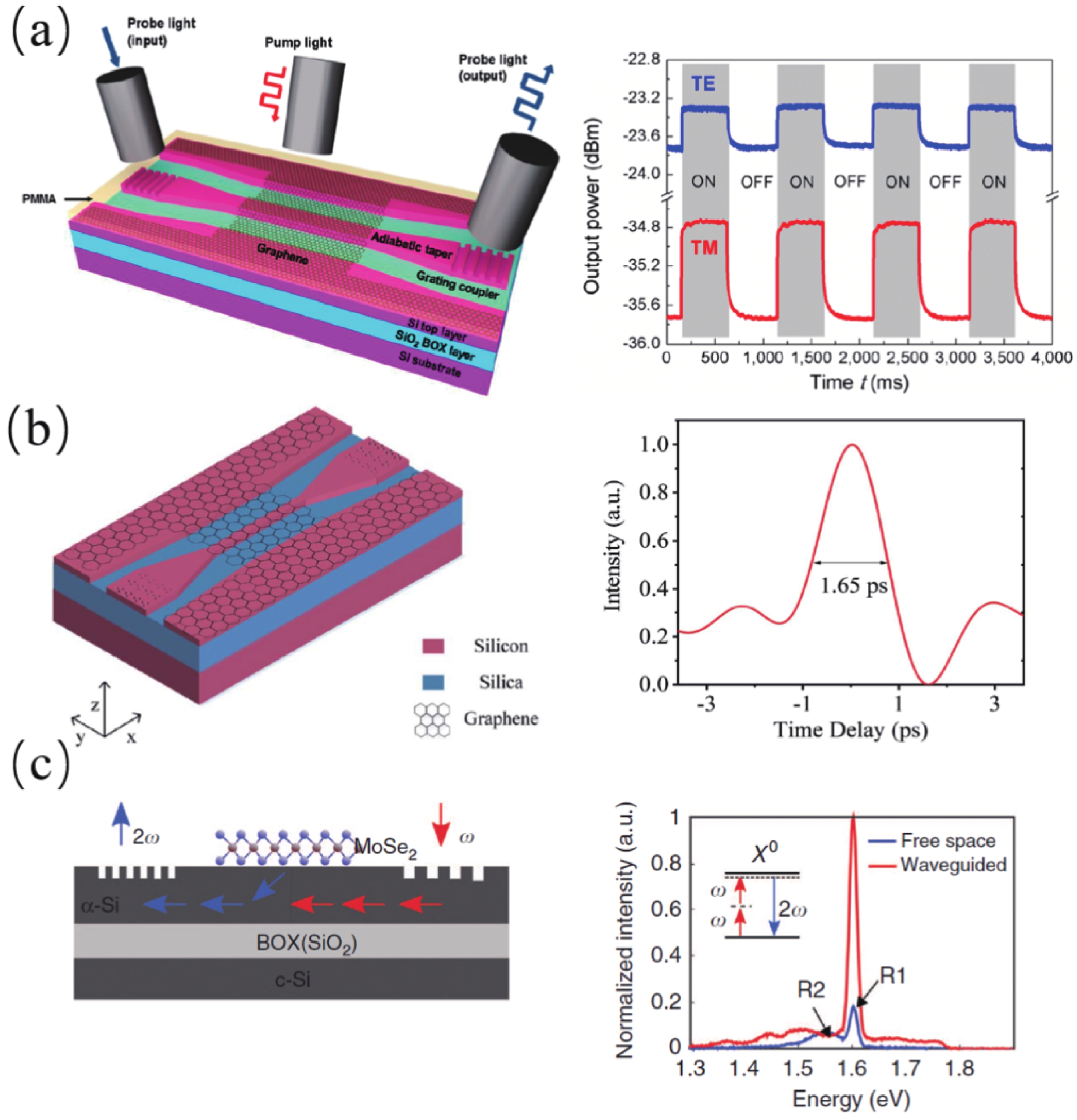
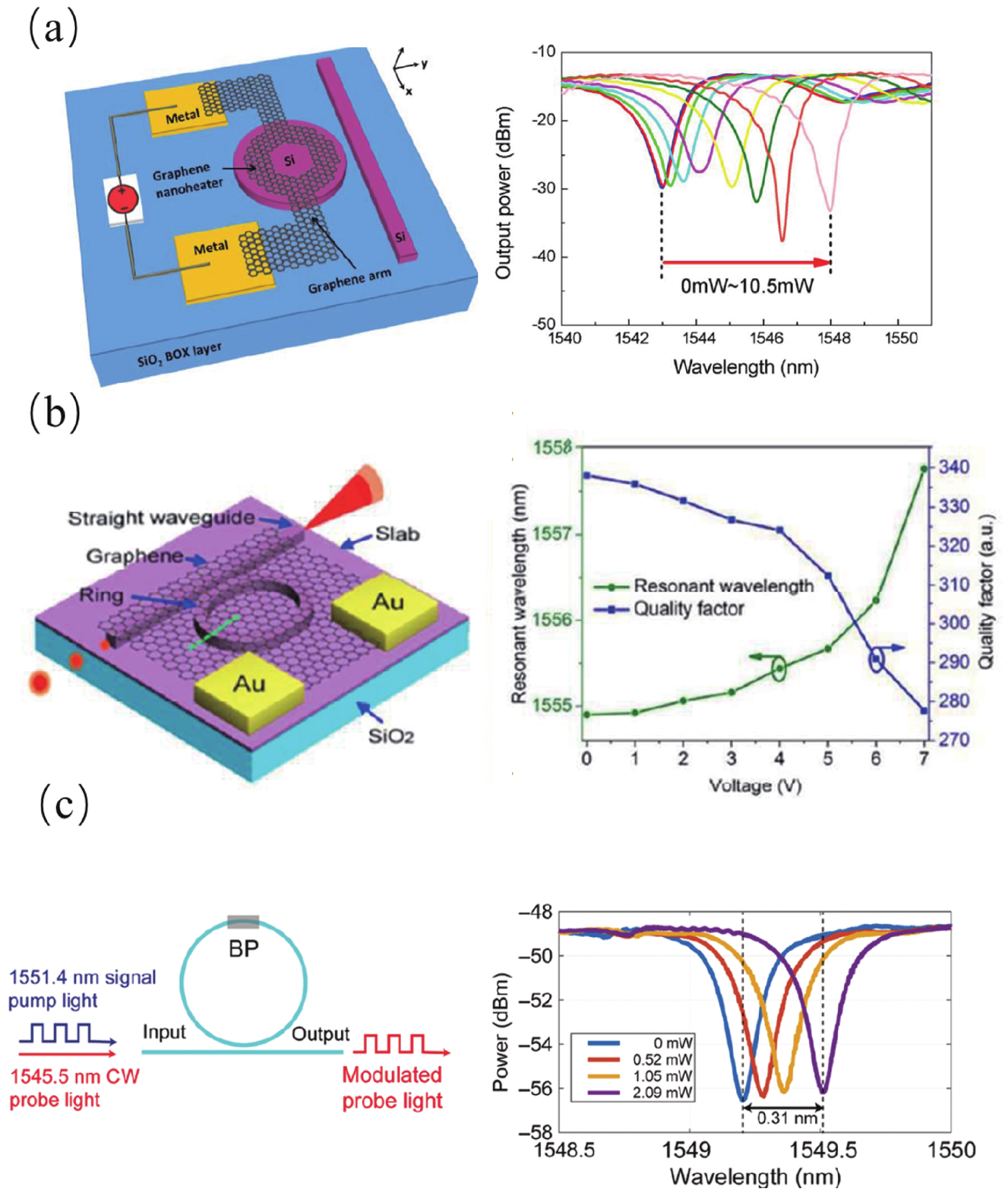
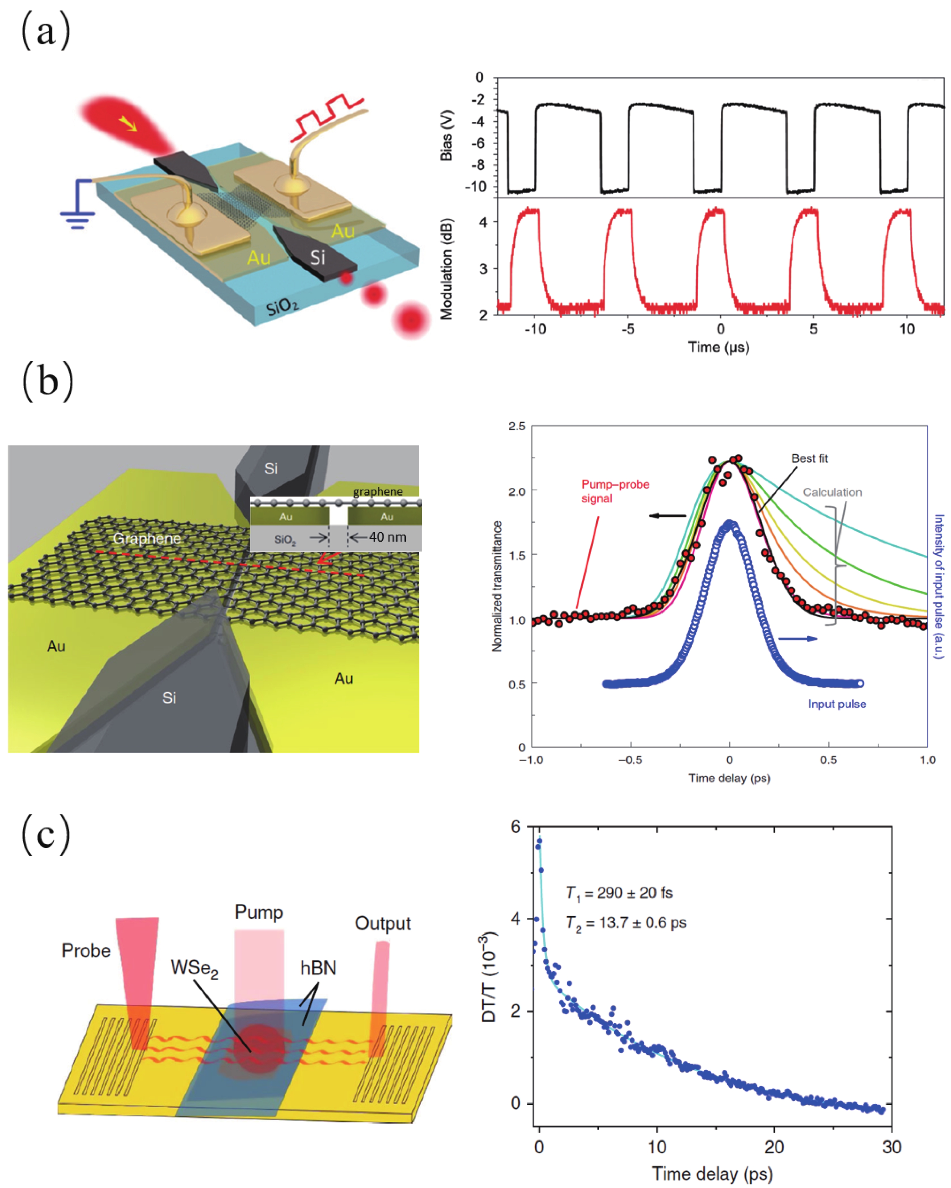
Waveguide-integrated optical modulators are indispensable for on-chip optical interconnects and optical computing. To cope with the ever-increasing amount of data being generated and consumed, ultrafast waveguide-integrated optical modulators with low energy consumption are highly demanded. In recent years, two-dimensional (2D) materials have attracted a lot of attention and have provided tremendous opportunities for the development of high-performance waveguide-integrated optical modulators because of their extraordinary optoelectronic properties and versatile compatibility. This paper reviews the state-of-the-art waveguide-integrated optical modulators with 2D materials, providing researchers with the developing trends in the field and allowing them to identify existing challenges and promising potential solutions. First, the concept and fundamental mechanisms of optical modulation with 2D materials are summarized. Second, a review of waveguide-integrated optical modulators employing electro-optic, all-optic, and thermo-optic effects is provided. Finally, the challenges and perspectives of waveguide-integrated modulators with 2D materials are discussed.

J. Semicond.
2023, 44(11): 111701 doi: 10.1088/1674-4926/44/11/111701

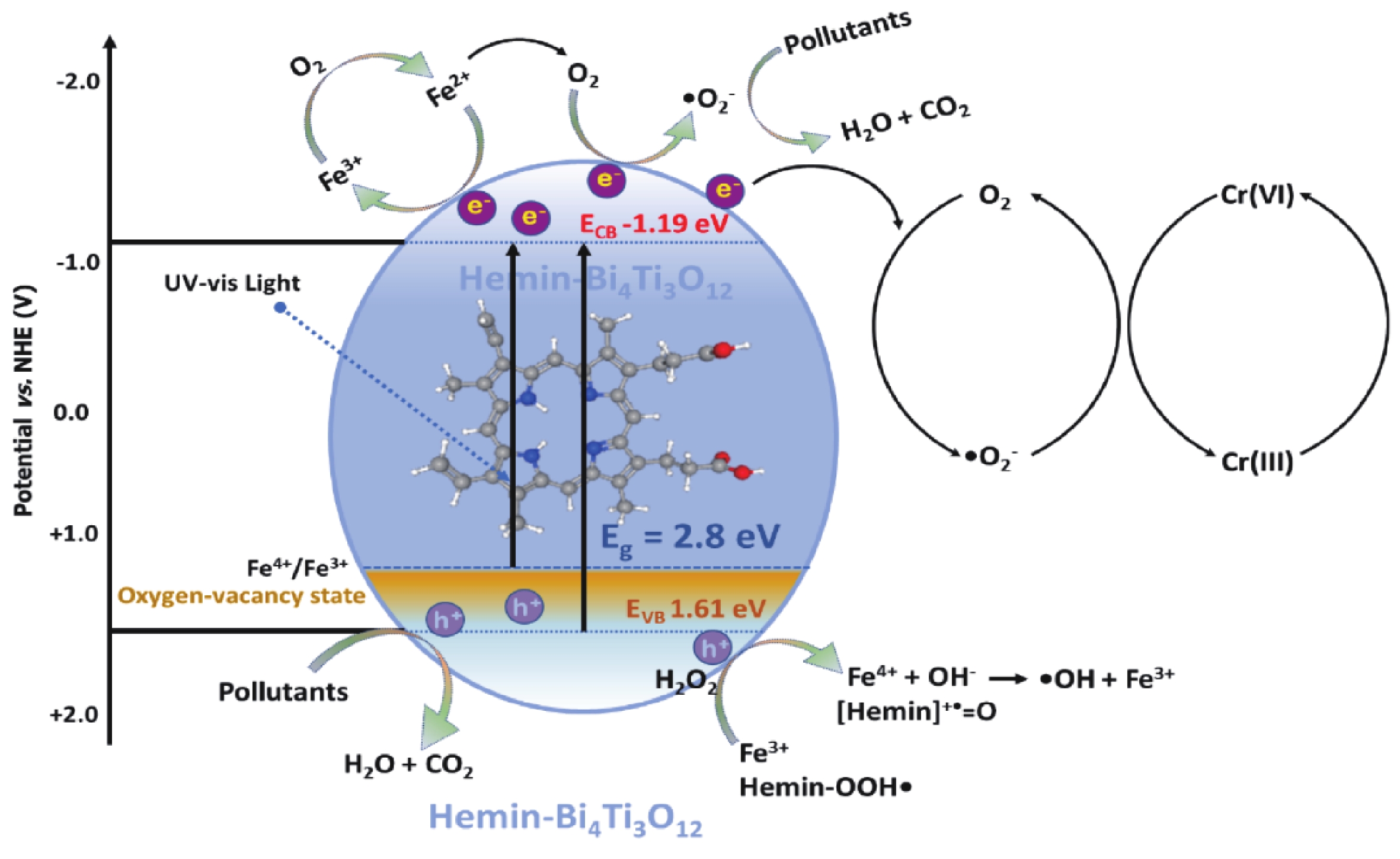
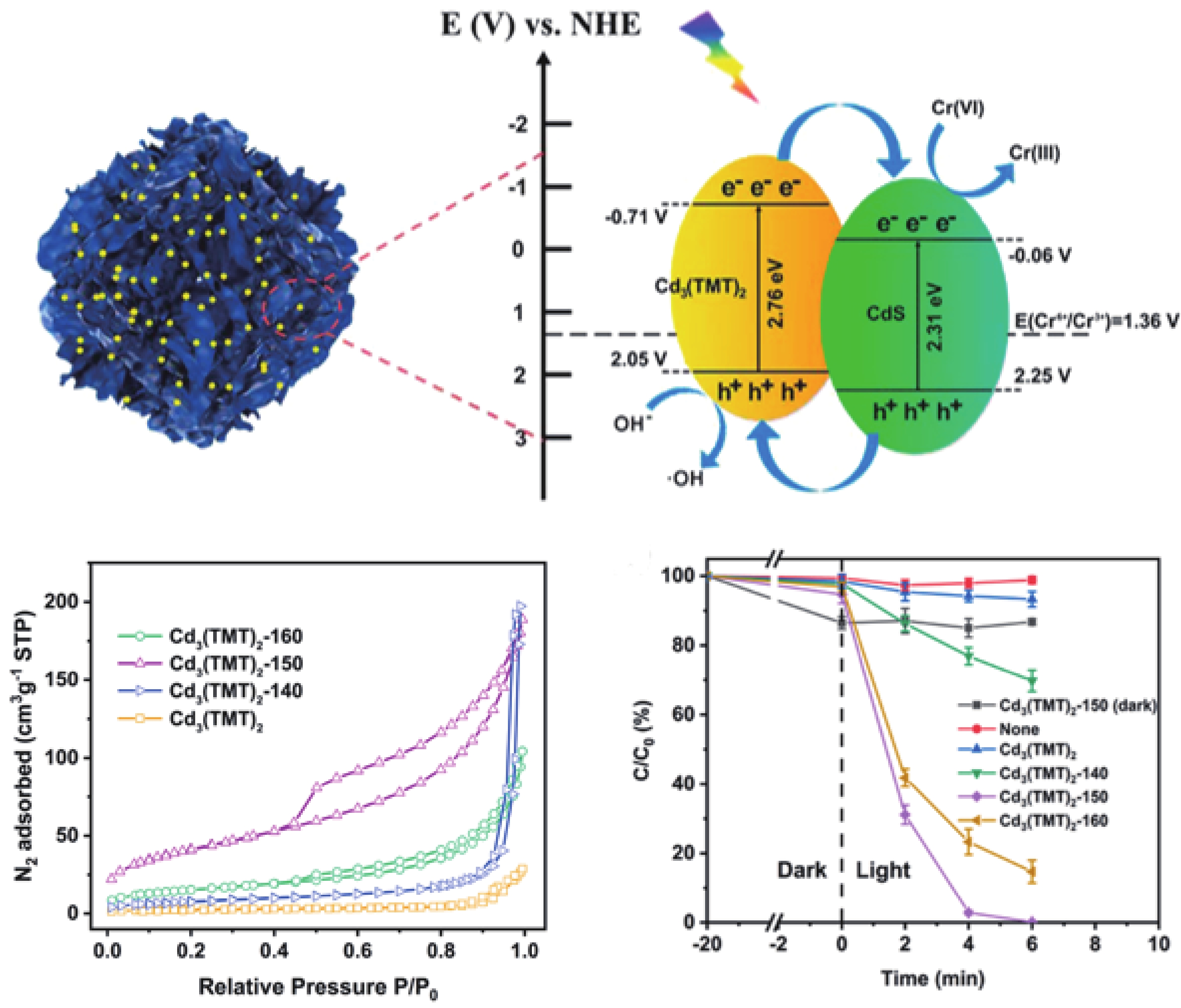
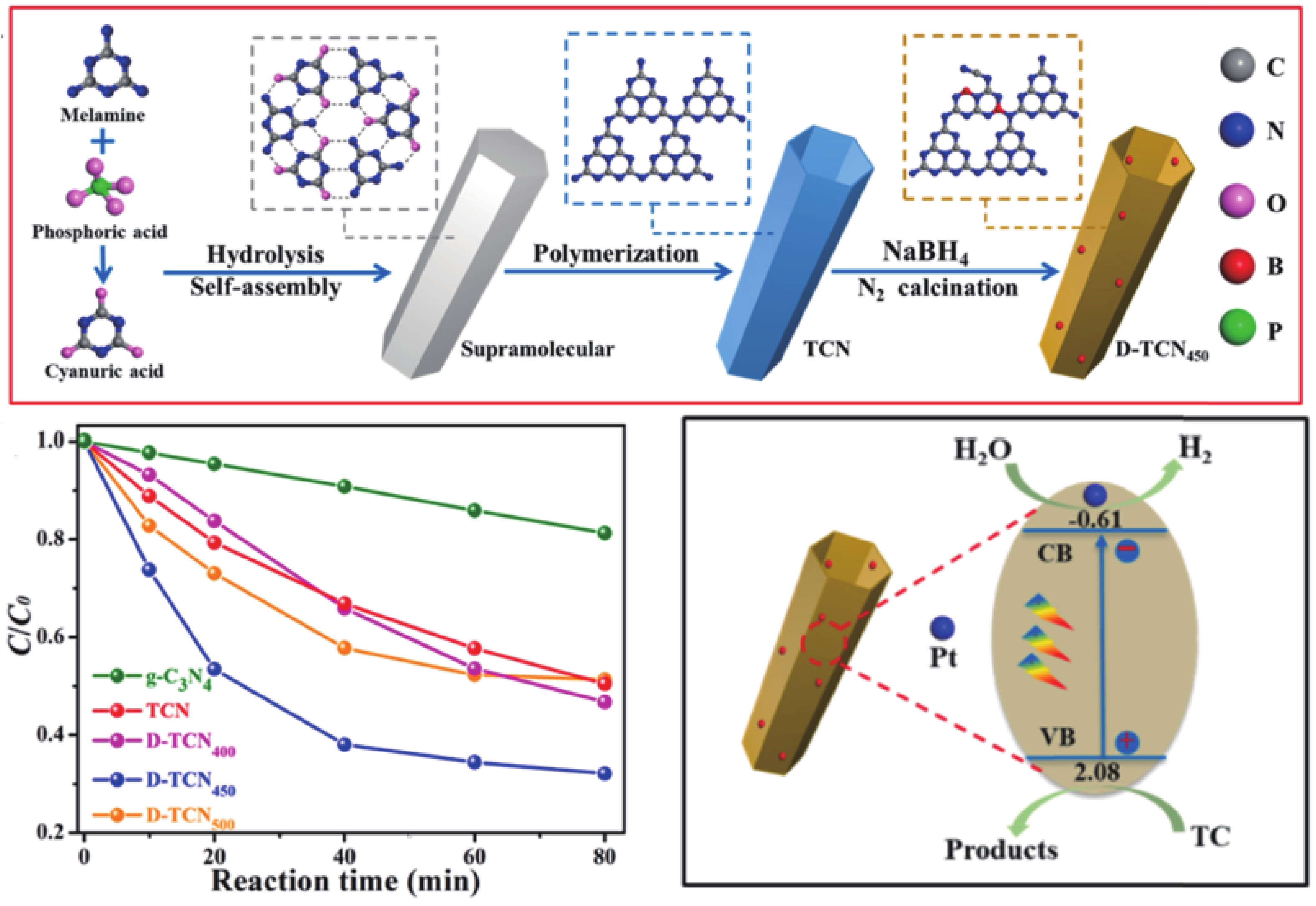
In recent years, the treatment of agricultural wastewater has been an important aspect of environmental protection. The purpose of photocatalytic technology is to degrade pollutants by utilizing solar light energy to stimulate the migration of photocarriers to the surface of photocatalysts and occur reduction-oxidation reaction with pollutants in agricultural wastewater. Photocatalytic technology has the characteristics of high efficiency, sustainability, low-energy and free secondary pollution. It is an environmental and economical method to recover water quality that only needs sunlight. In this paper, the mechanism and research progress of photocatalytic removal of heavy metal ions and antibiotics from agricultural water pollution were reviewed by combining photocatalytic degradation process with agricultural treatment technology. The mechanism of influencing factors of photocatalytic degradation efficiency was discussed in detail and corresponding strategies were proposed, which has certain reference value for the development of photocatalytic degradation.


J. Semicond.
2023, 44(11): 113101 doi: 10.1088/1674-4926/44/11/113101
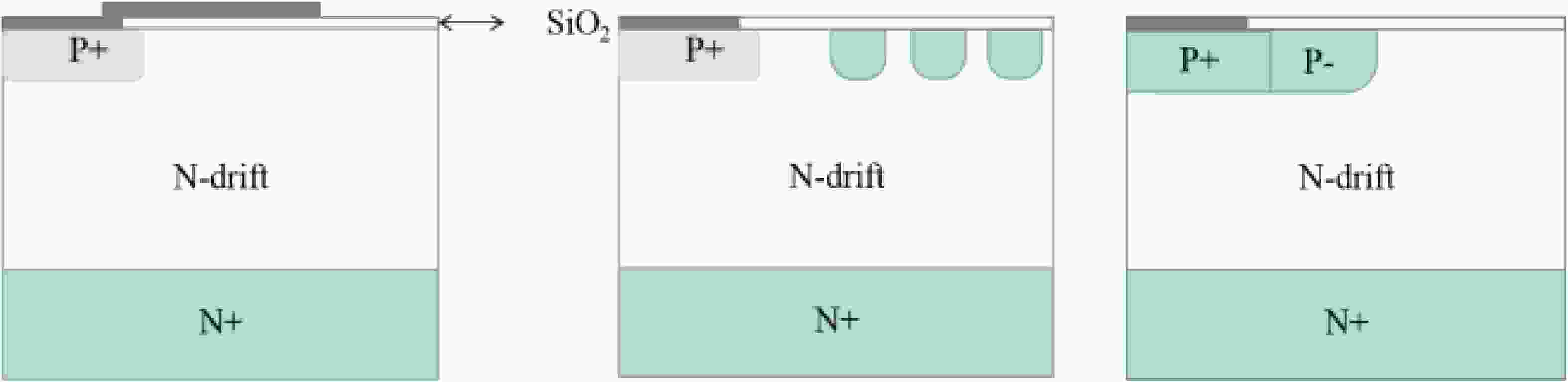
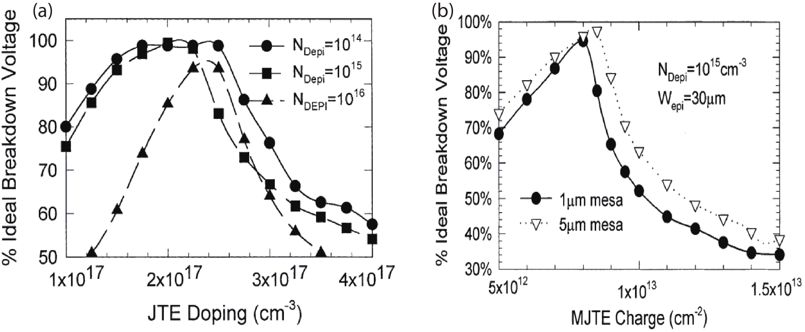
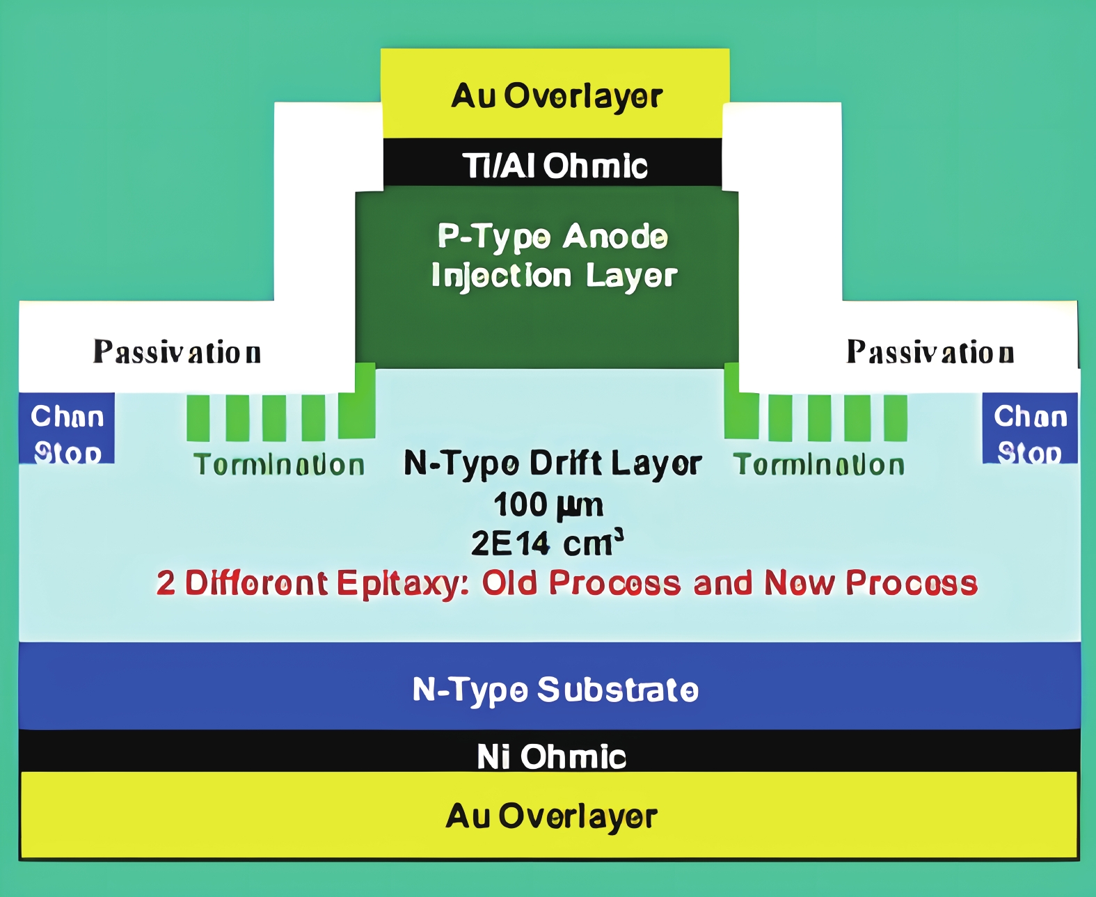
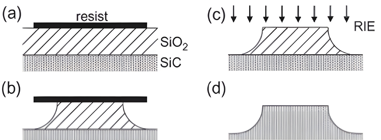
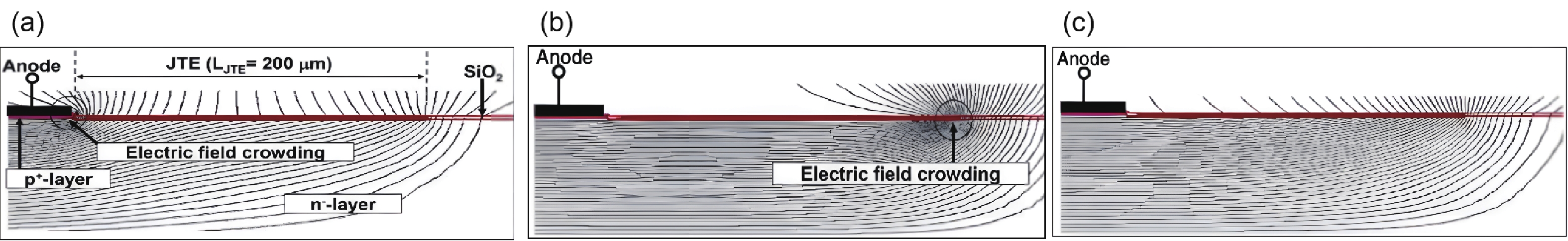
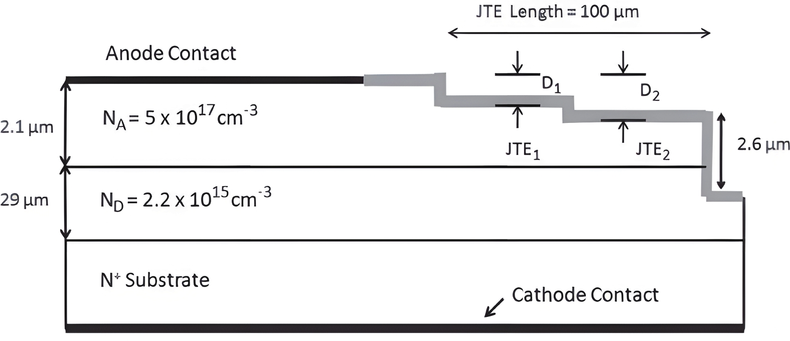
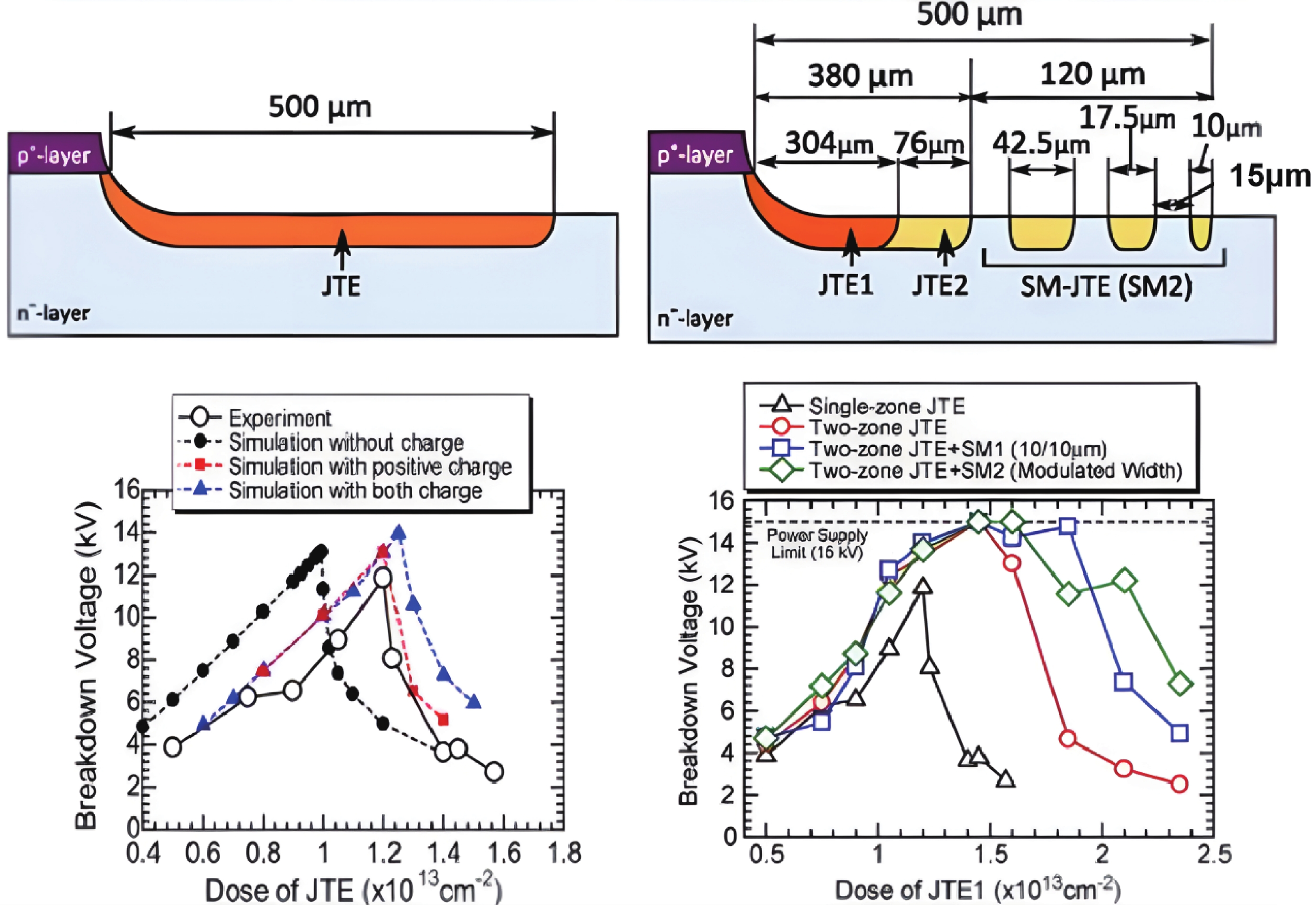
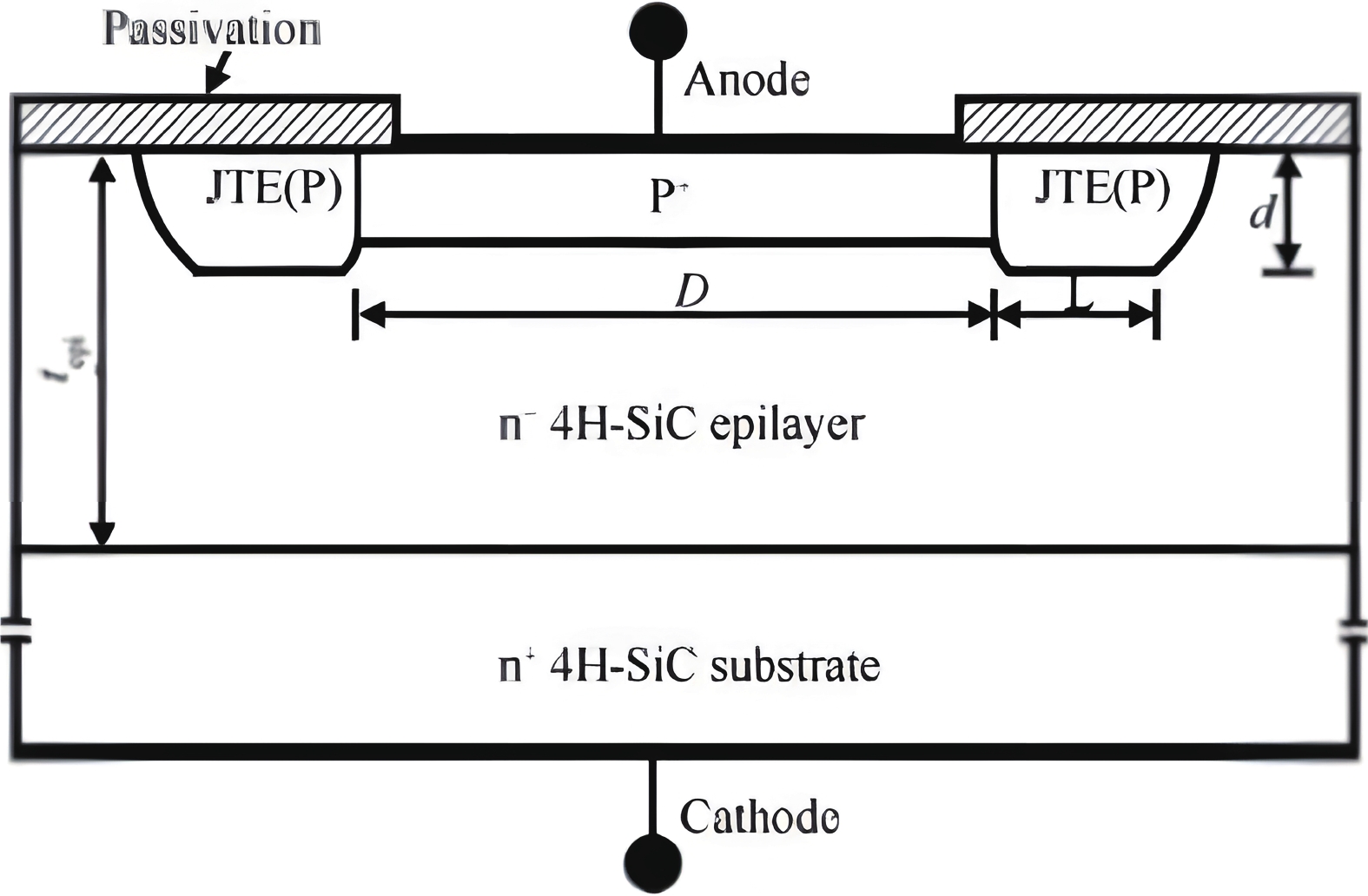
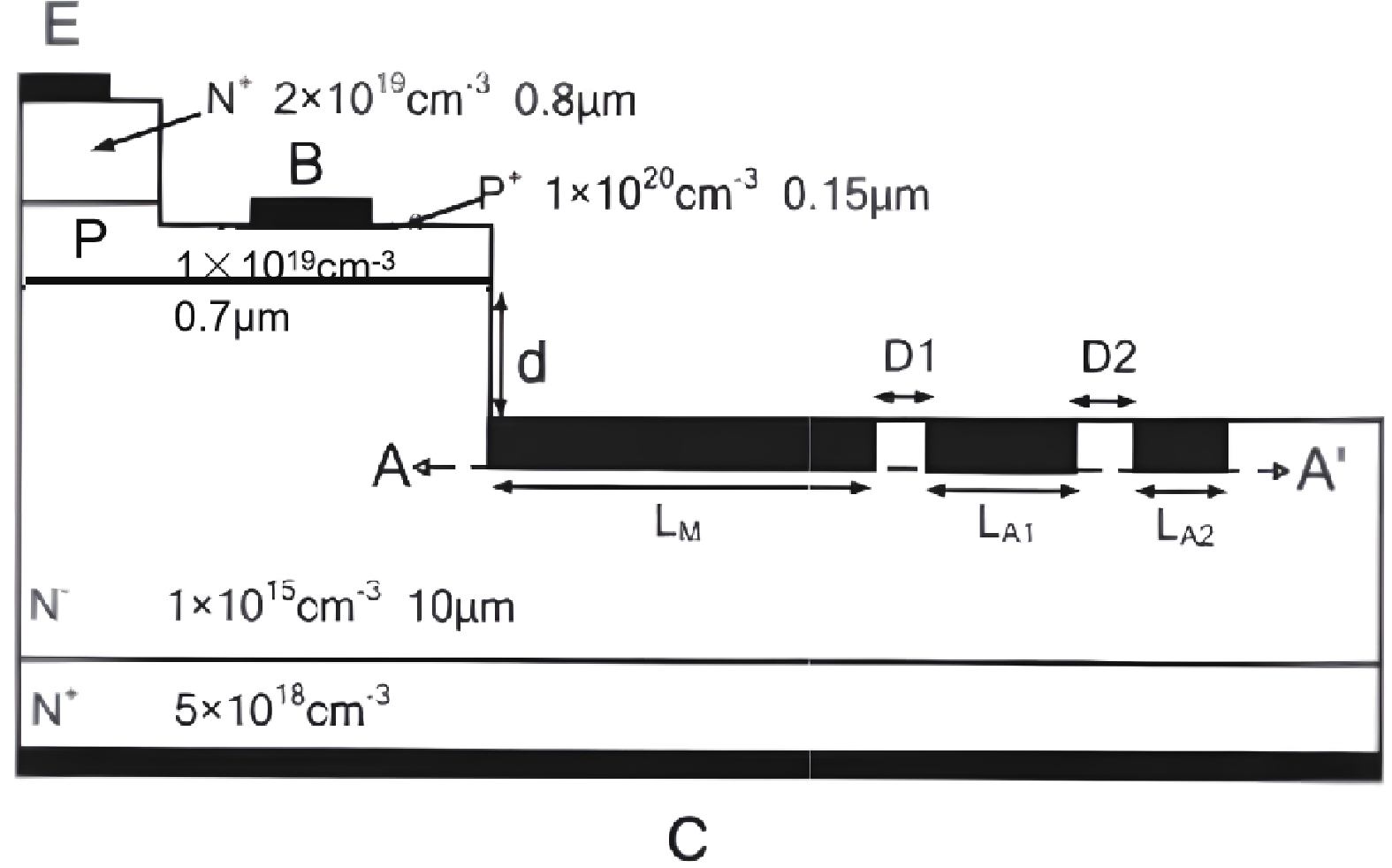
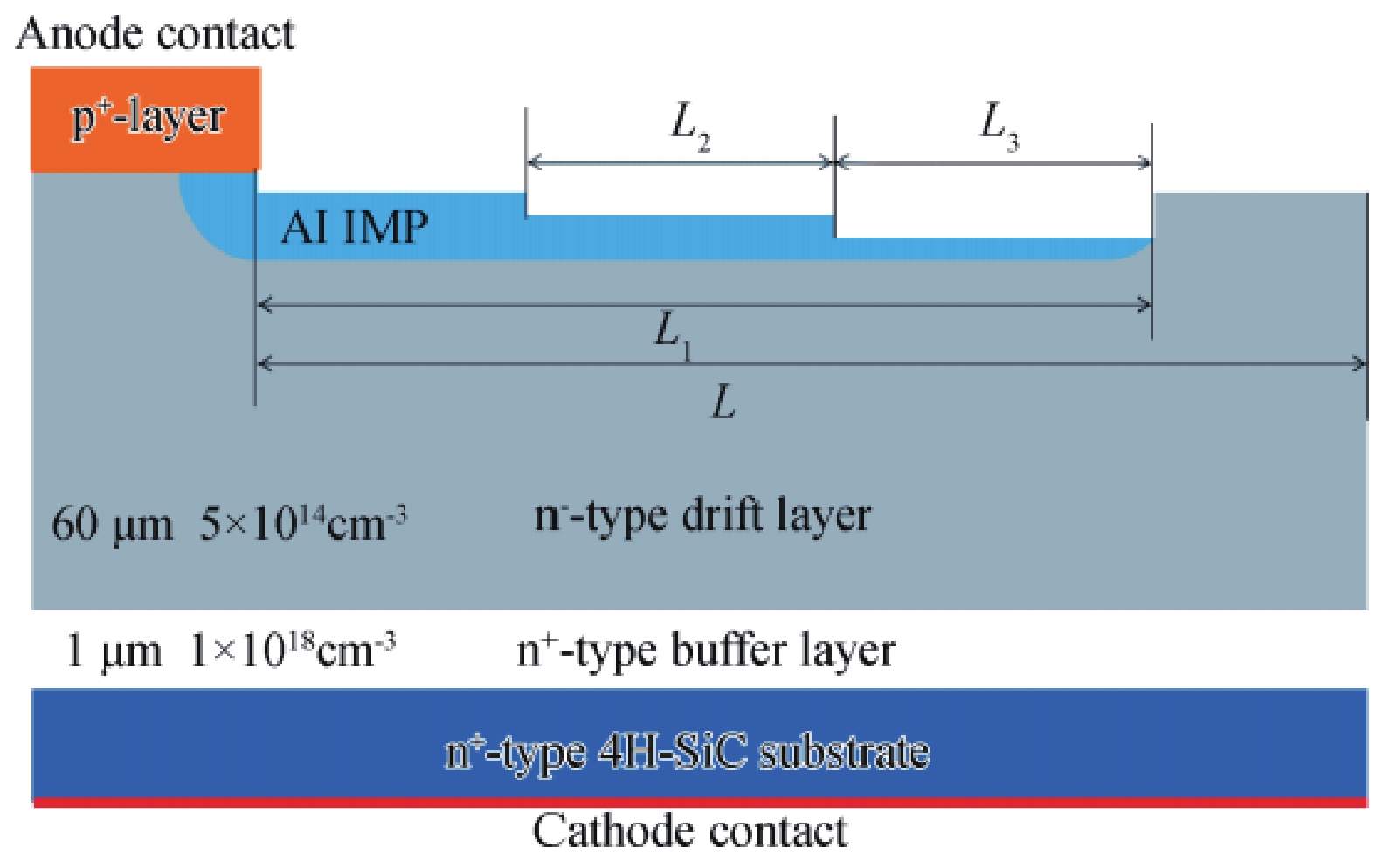
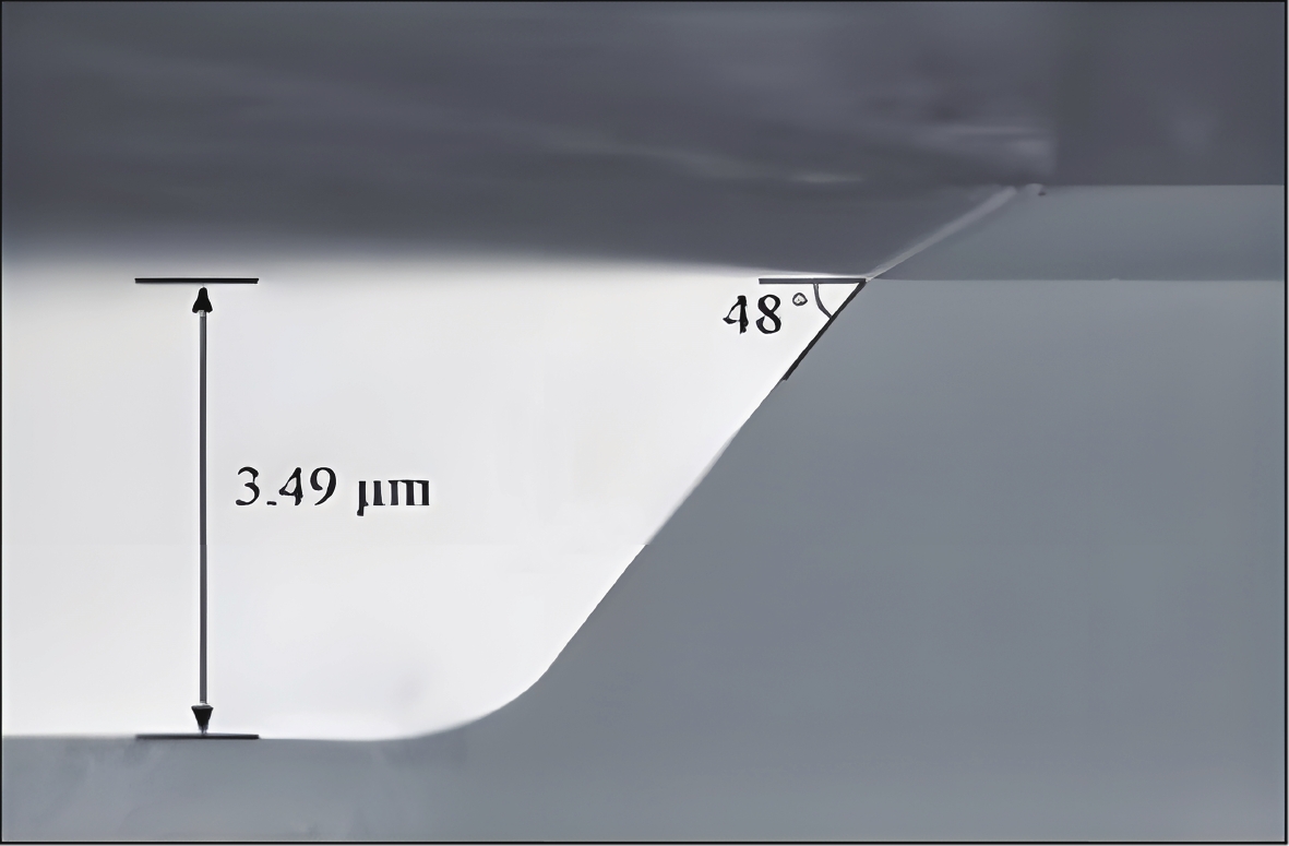
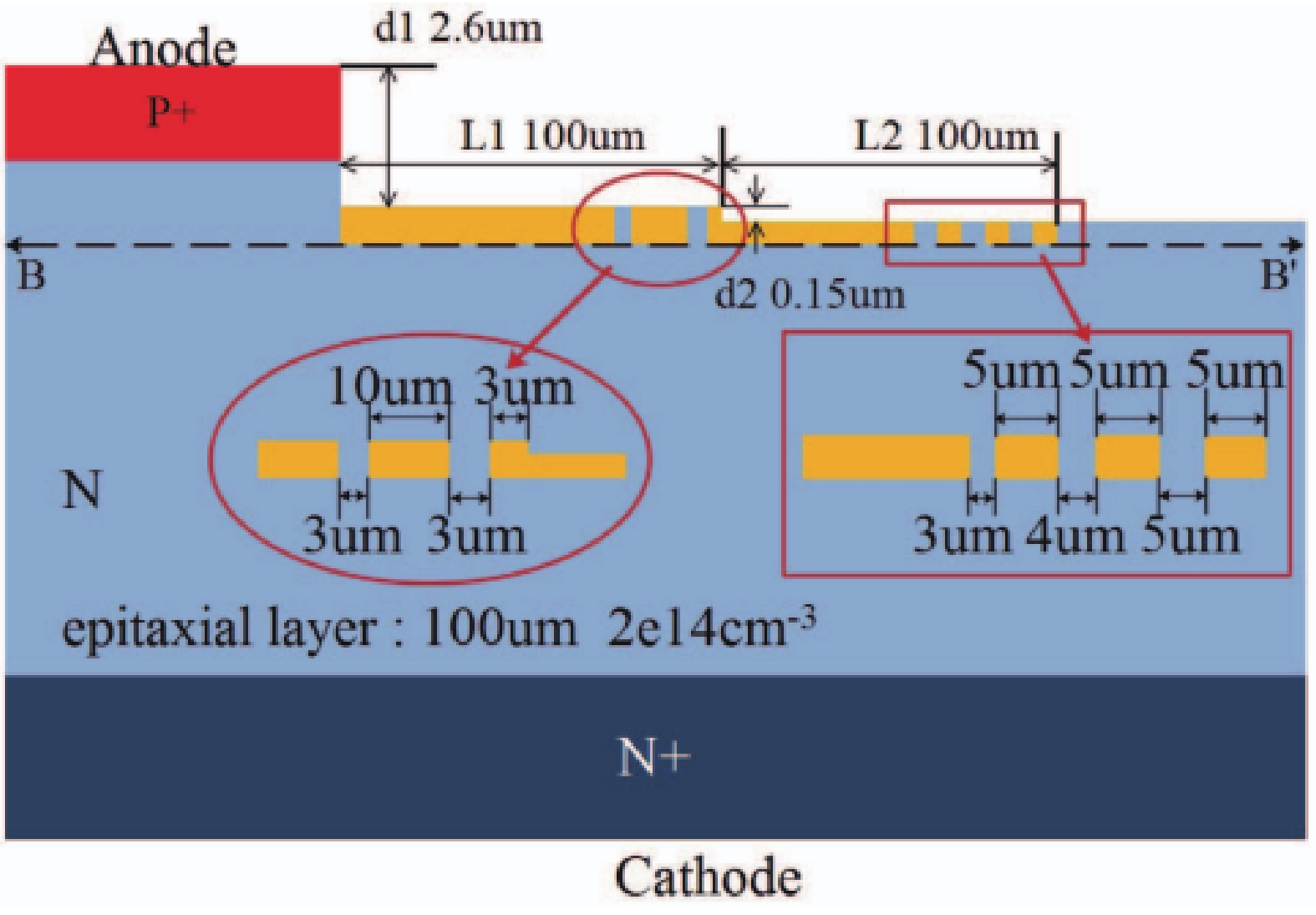
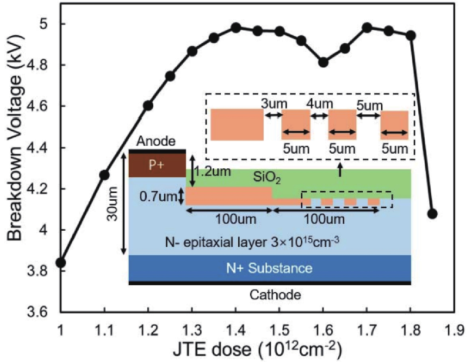
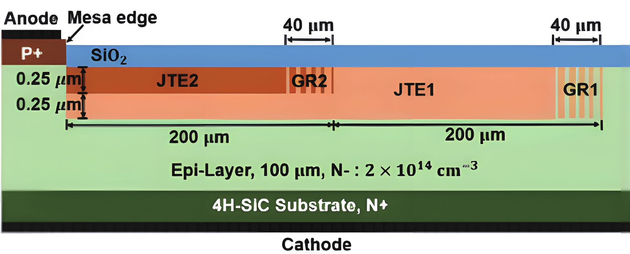
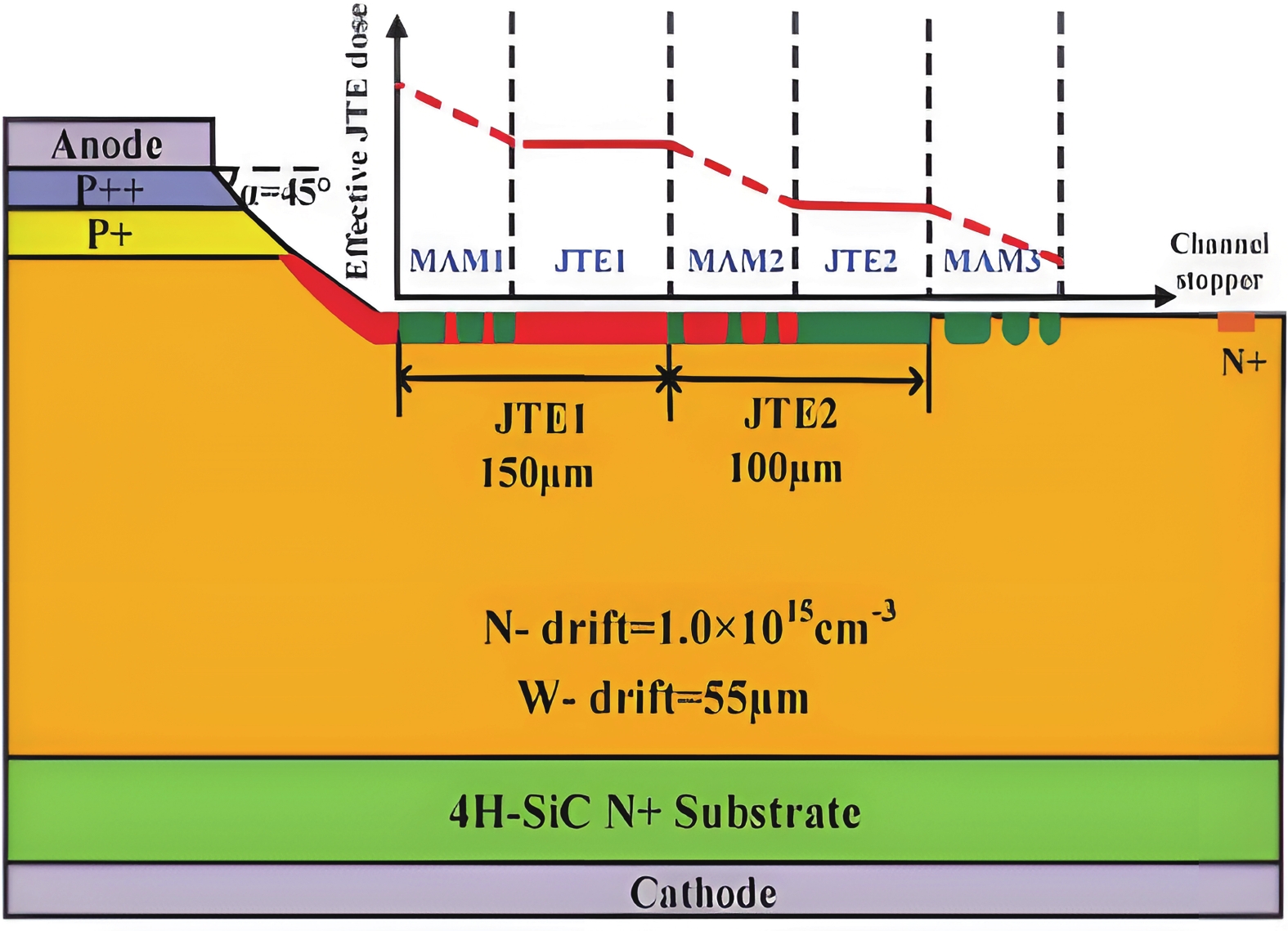
The comparison of domestic and foreign studies has been utilized to extensively employ junction termination extension (JTE) structures for power devices. However, achieving a gradual doping concentration change in the lateral direction is difficult for SiC devices since the diffusion constants of the implanted aluminum ions in SiC are much less than silicon. Many previously reported studies adopted many new structures to solve this problem. Additionally, the JTE structure is strongly sensitive to the ion implantation dose. Thus, GA-JTE, double-zone etched JTE structures, and SM-JTE with modulation spacing were reported to overcome the above shortcomings of the JTE structure and effectively increase the breakdown voltage. They provided a theoretical basis for fabricating terminal structures of 4H-SiC PiN diodes. This paper summarized the effects of different terminal structures on the electrical properties of SiC devices at home and abroad. Presently, the continuous development and breakthrough of terminal technology have significantly improved the breakdown voltage and terminal efficiency of 4H-SiC PiN power diodes.


J. Semicond.
2023, 44(11): 112001 doi: 10.1088/1674-4926/44/11/112001
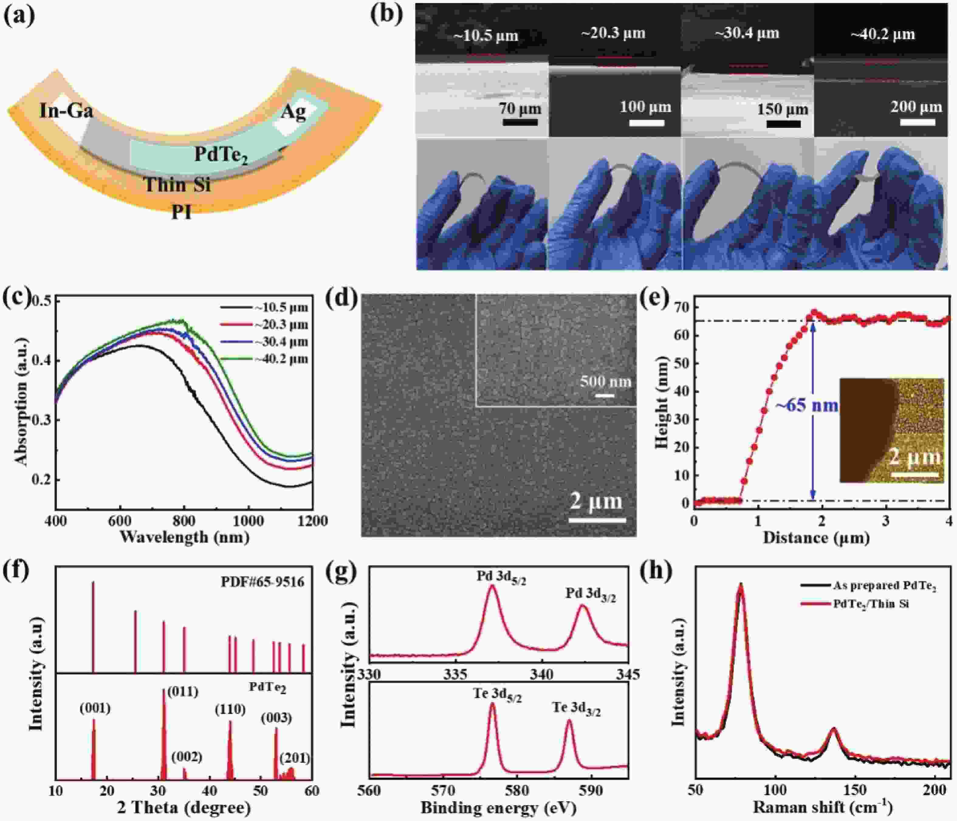
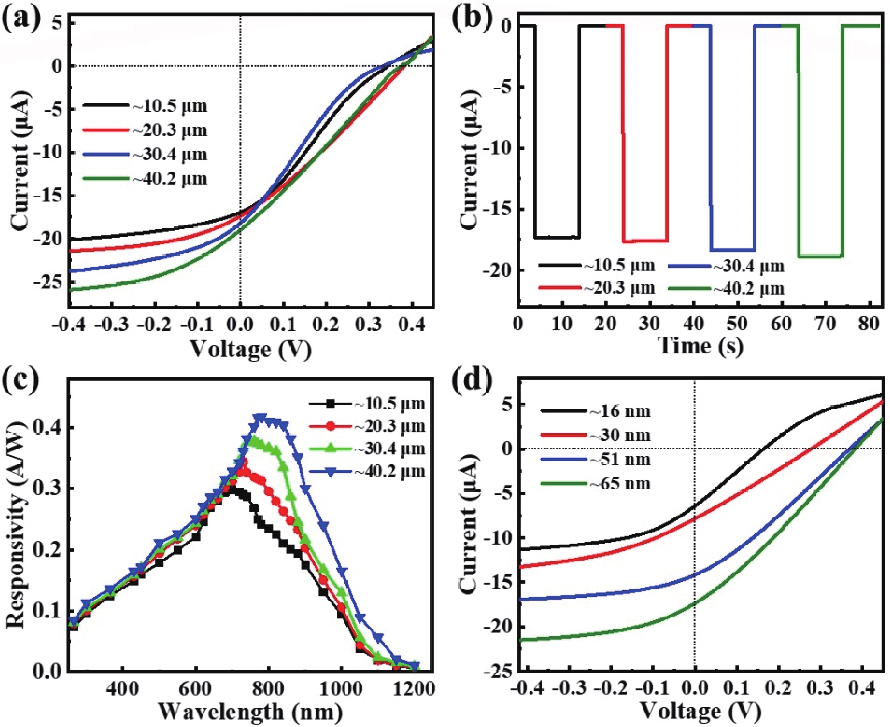
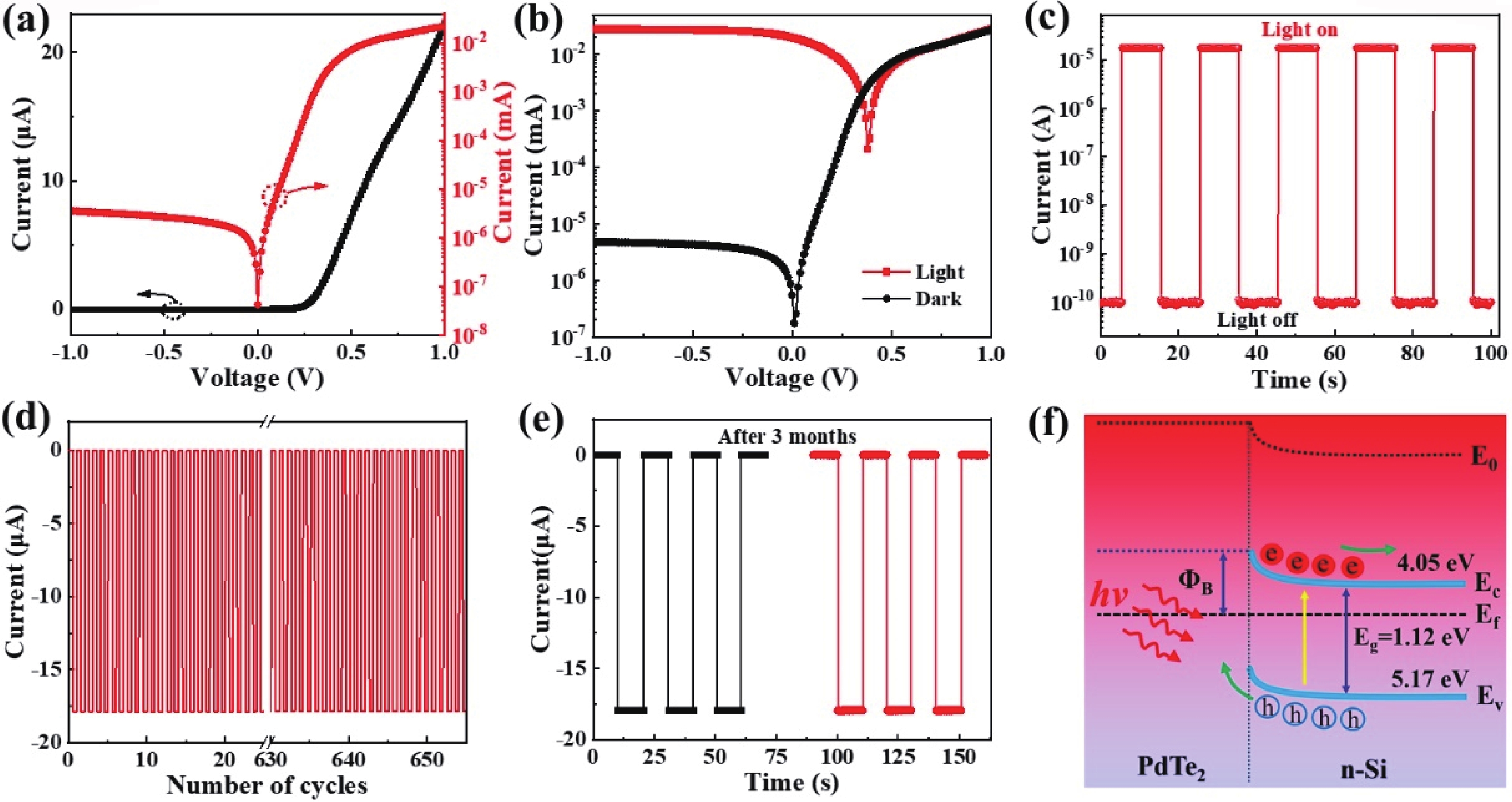
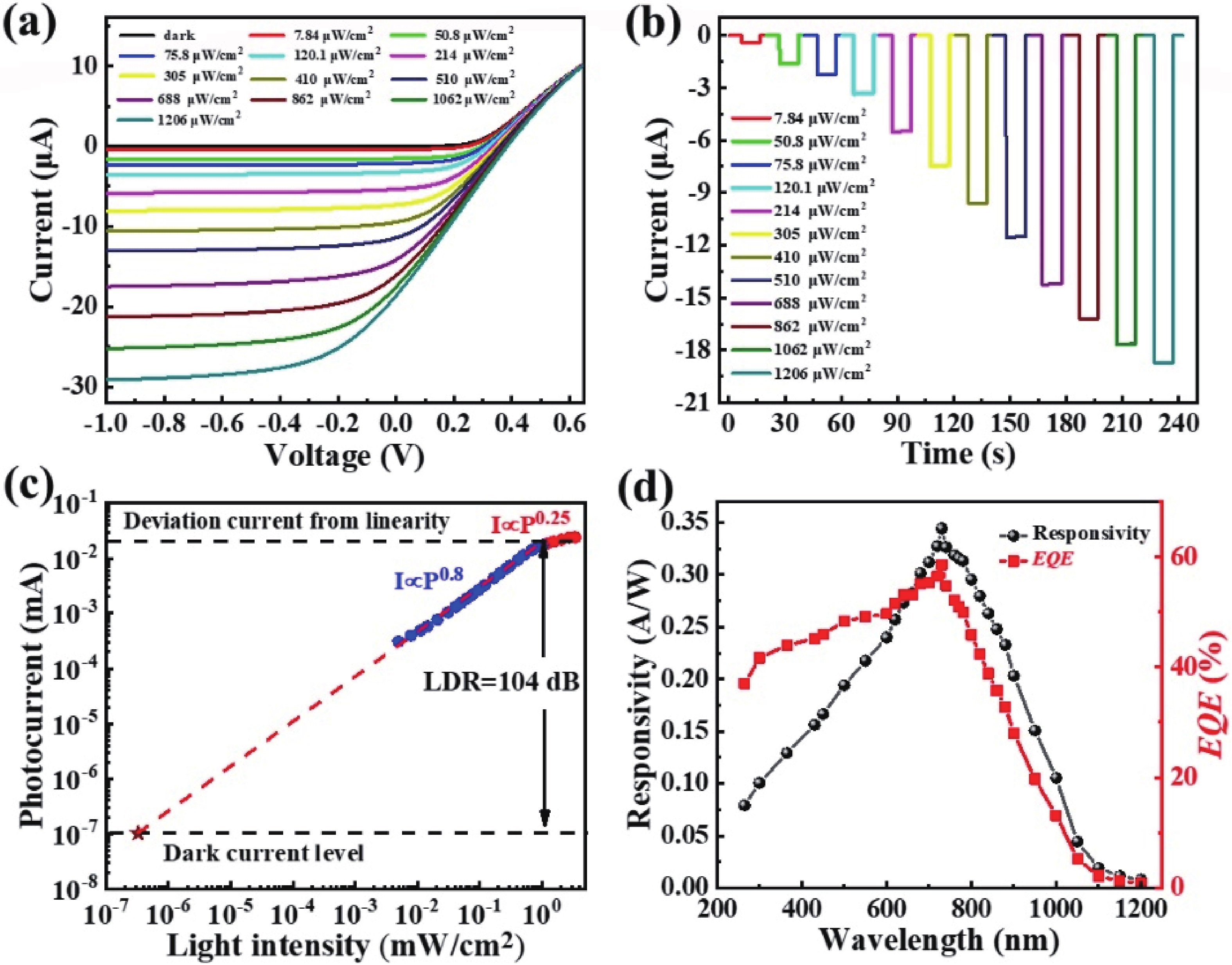
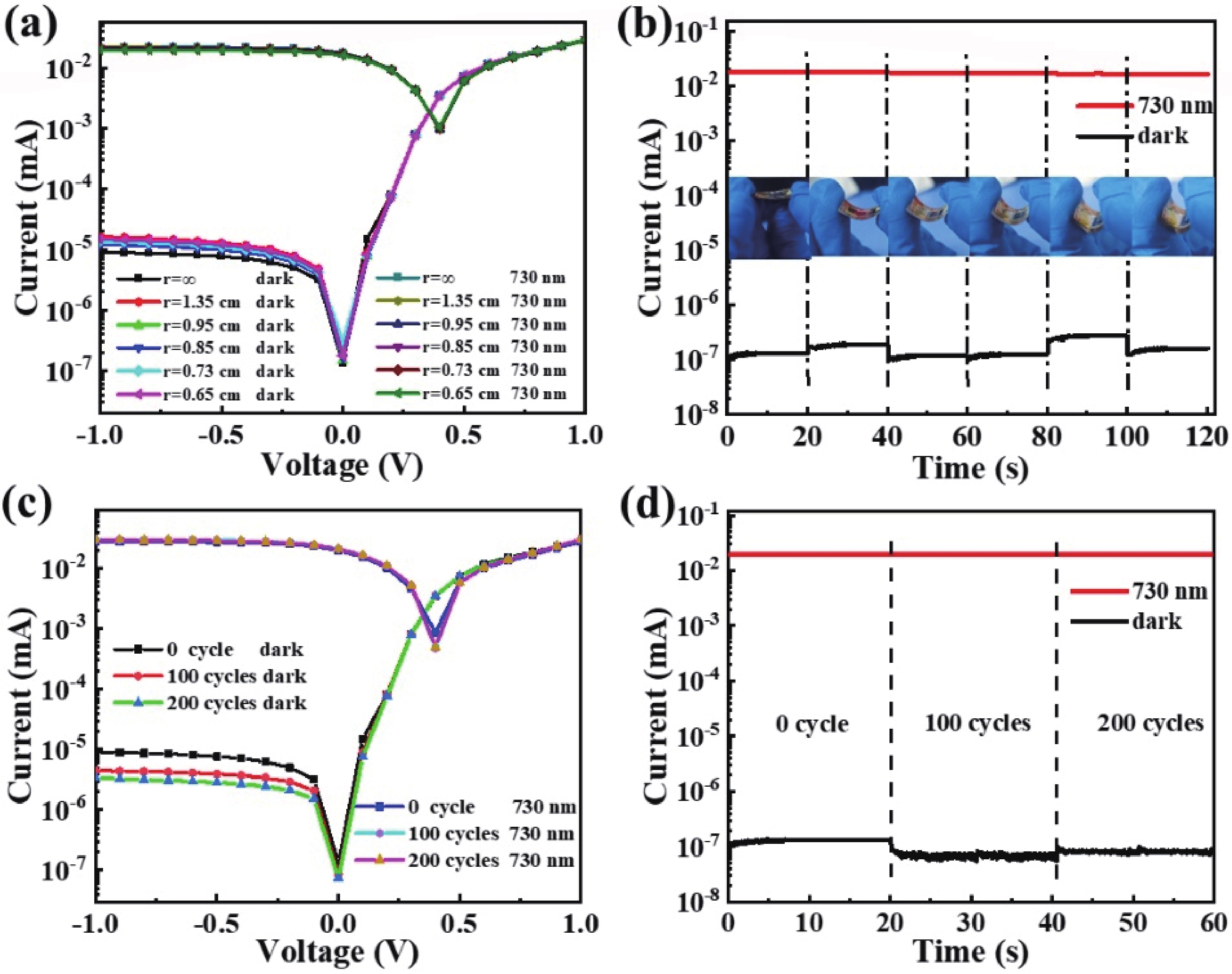
Two-dimensional layered material/semiconductor heterostructures have emerged as a category of fascinating architectures for developing highly efficient and low-cost photodetection devices. Herein, we present the construction of a highly efficient flexible light detector operating in the visible-near infrared wavelength regime by integrating a PdTe2 multilayer on a thin Si film. A representative device achieves a good photoresponse performance at zero bias including a sizeable current on/off ratio exceeding 105, a decent responsivity of ~343 mA/W, a respectable specific detectivity of ~2.56 × 10¹² Jones, and a rapid response time of 4.5/379 μs, under 730 nm light irradiation. The detector also displays an outstanding long-term air stability and operational durability. In addition, thanks to the excellent flexibility, the device can retain its prominent photodetection performance at various bending radii of curvature and upon hundreds of bending tests. Furthermore, the large responsivity and rapid response speed endow the photodetector with the ability to accurately probe heart rate, suggesting a possible application in the area of flexible and wearable health monitoring.


J. Semicond.
2023, 44(11): 112301 doi: 10.1088/1674-4926/44/11/112301
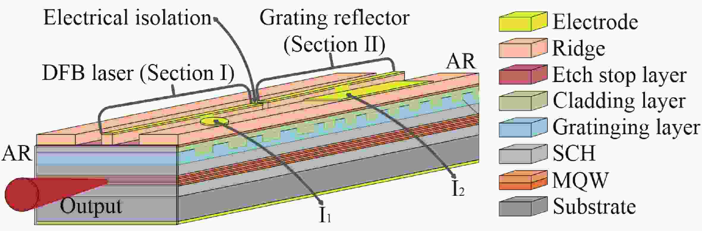
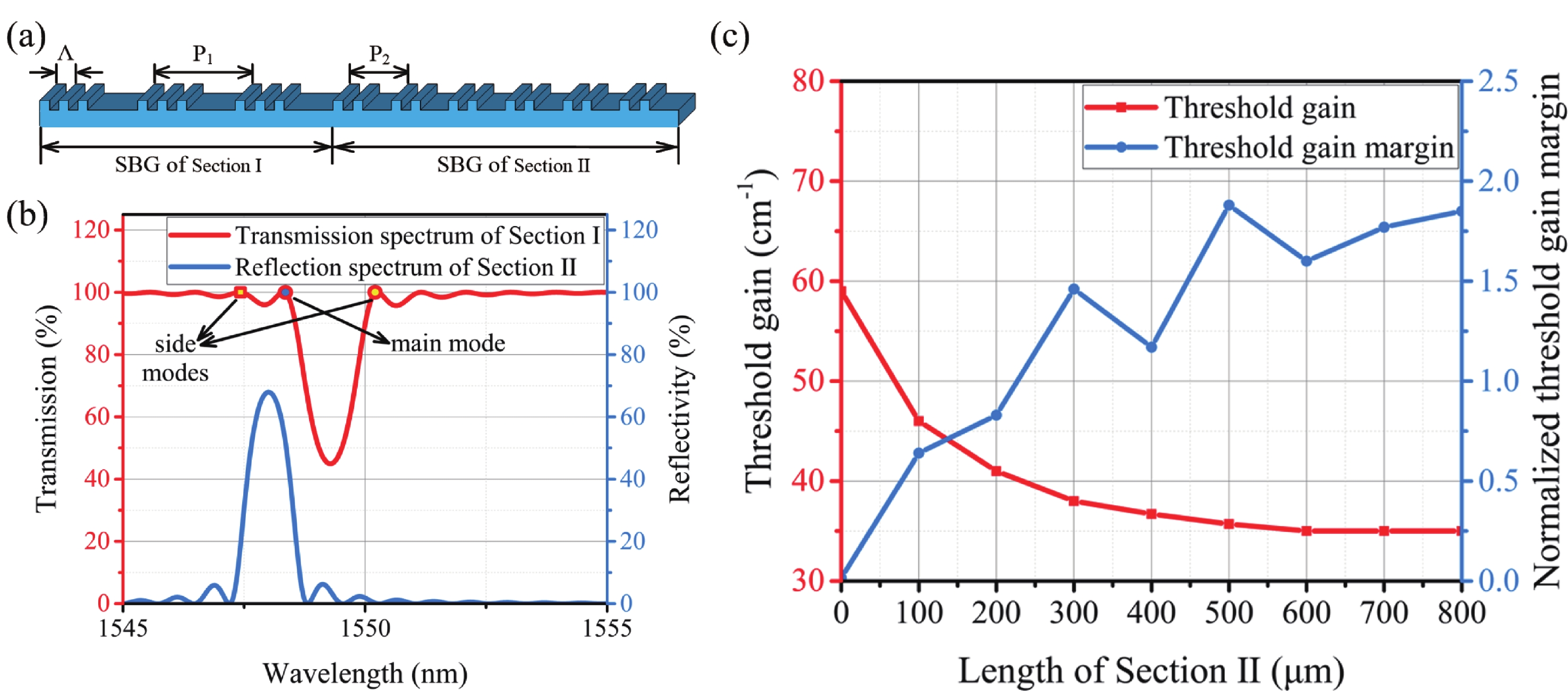
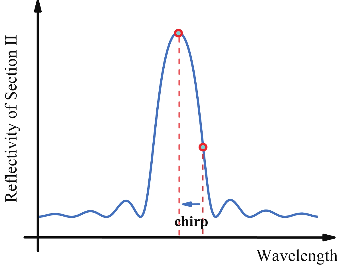
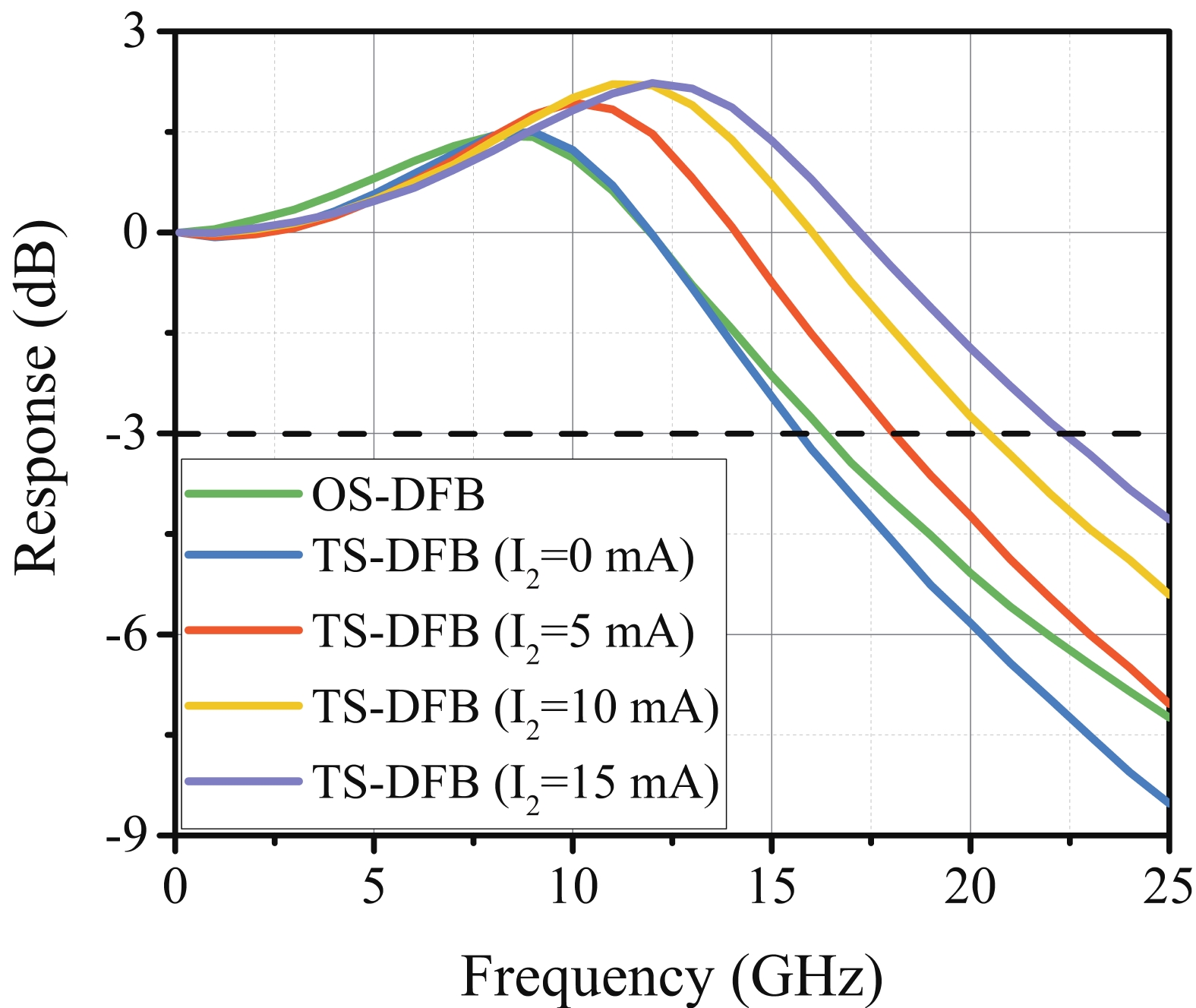
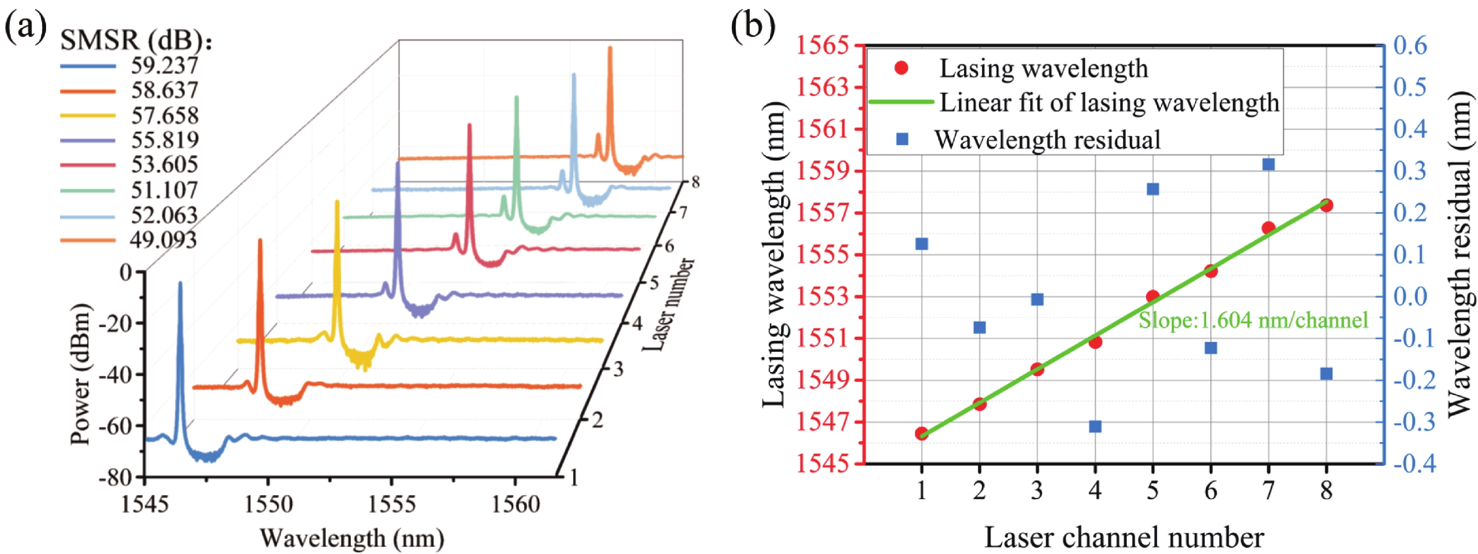
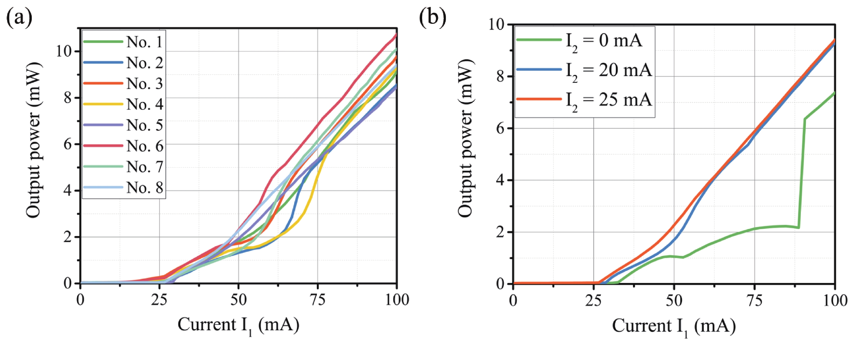
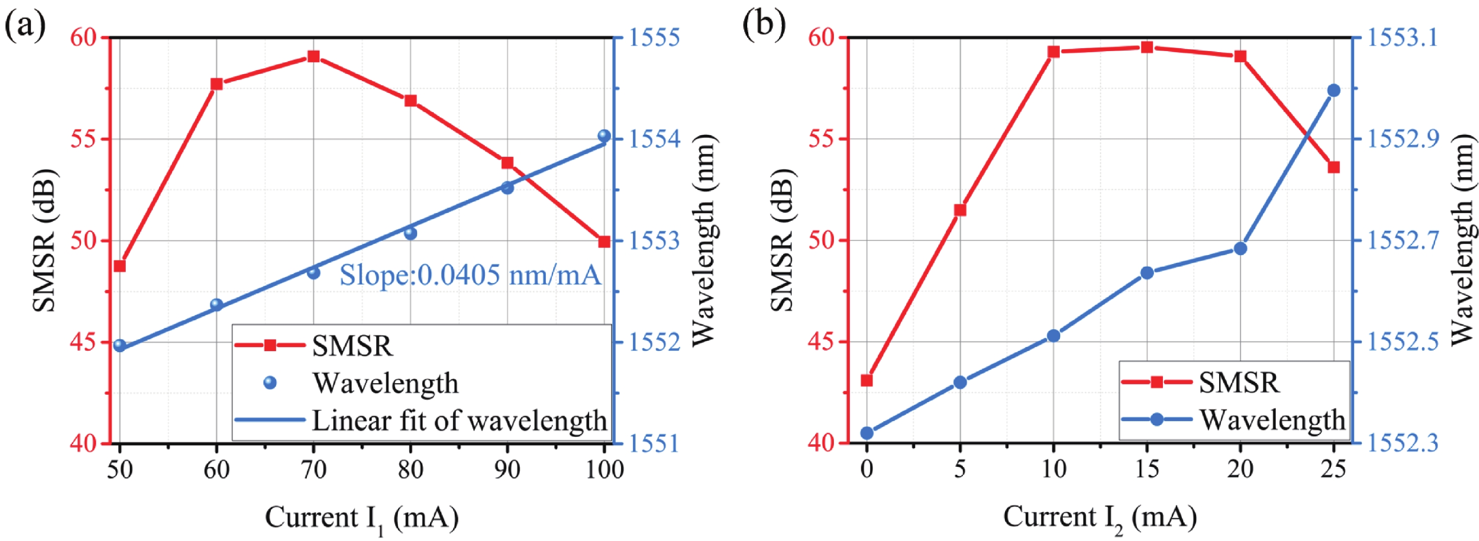
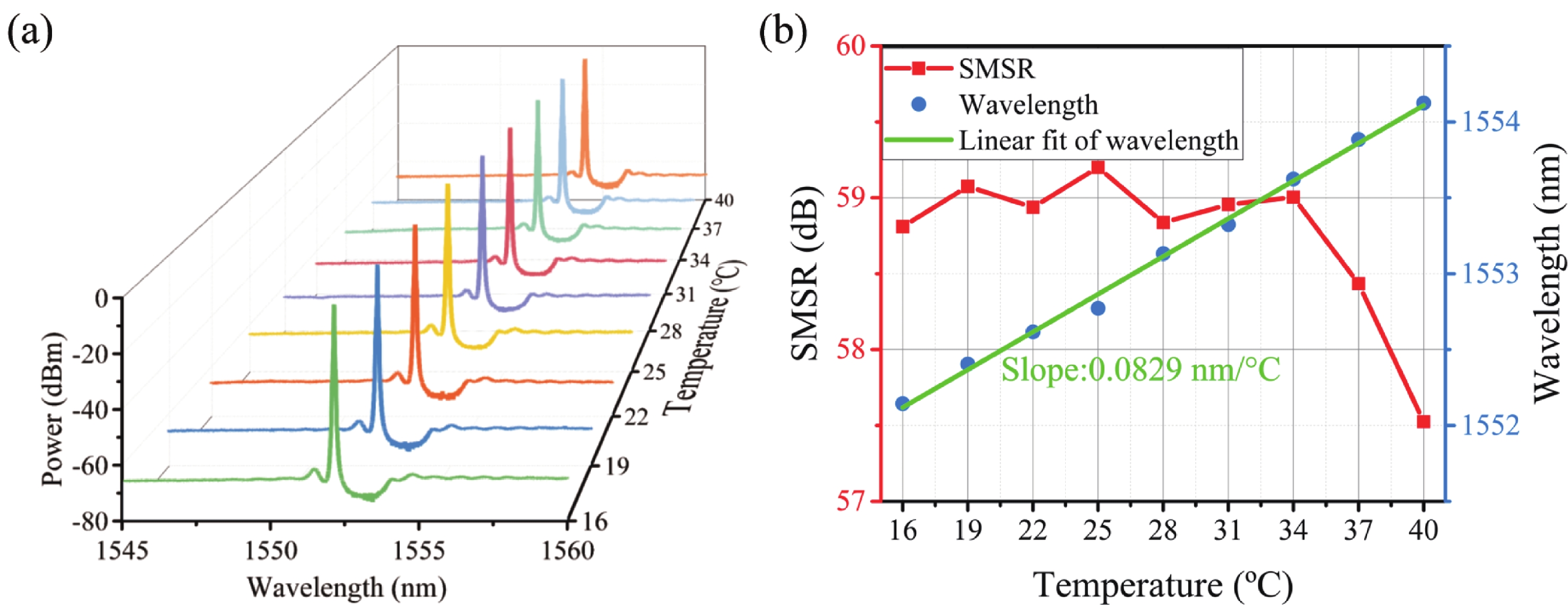
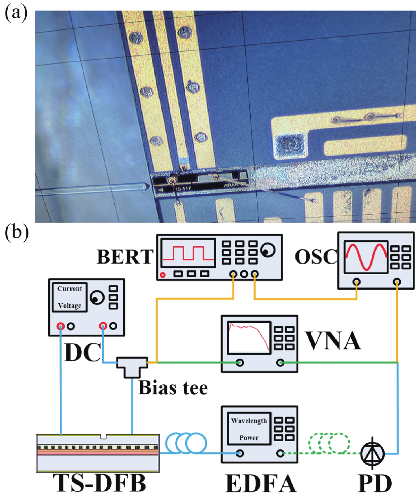
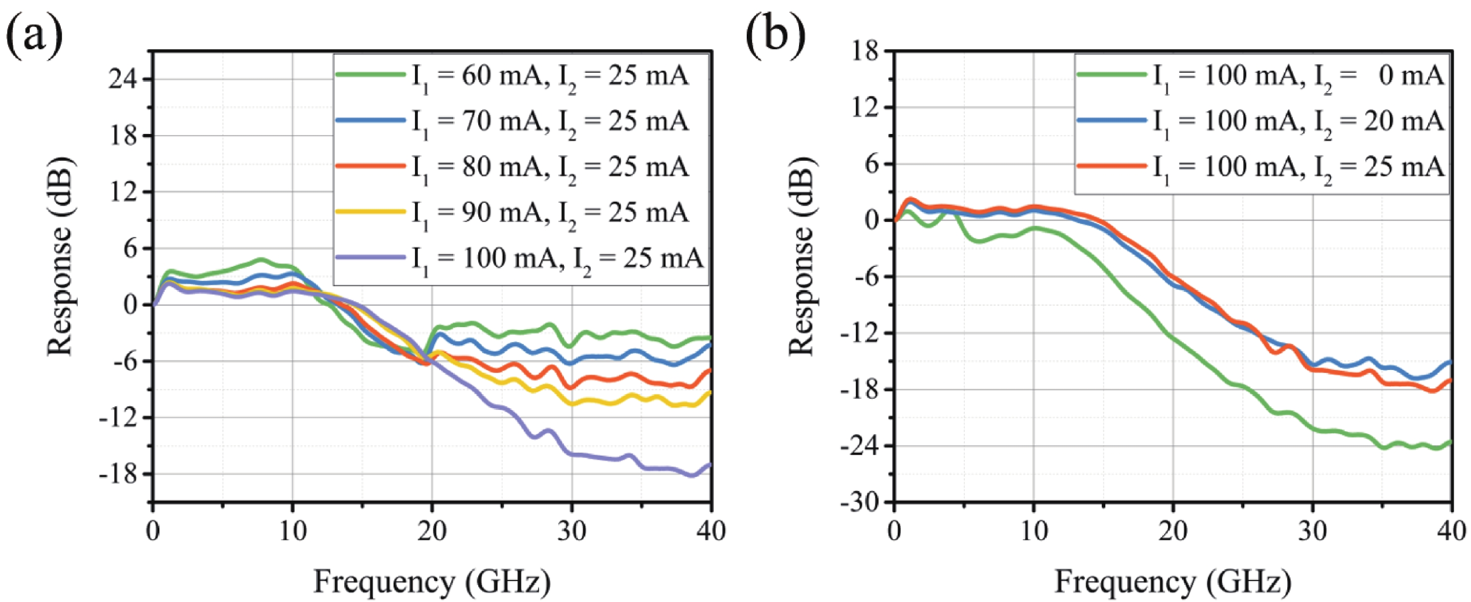
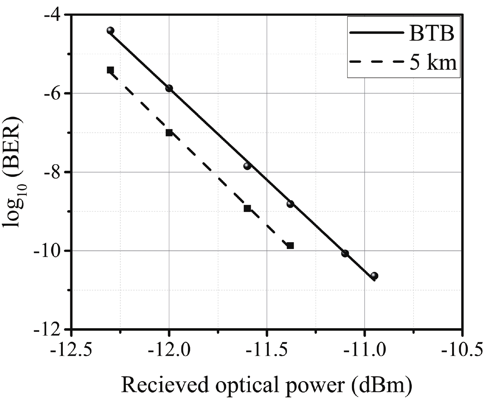
Modulation bandwidth enhancement in a directly modulated two-section distributed feedback (TS-DFB) laser based on a detuned loading effect is investigated and experimentally demonstrated. The results show that the 3-dB bandwidth of the TS-DFB laser is increased to 17.6 GHz and that chirp parameter can be reduced to 2.24. Compared to the absence of a detuned loading effect, there is a 4.6 GHz increase and a 2.45 reduction, respectively. After transmitting a 10 Gb/s non-return-to-zero (NRZ) signal through a 5-km fiber, the modulation eye diagram still achieves a large opening. Eight-channel laser arrays with precise wavelength spacing are fabricated. Each TS-DFB laser in the array has side mode suppression ratios (SMSR) > 49.093 dB and the maximum wavelength residual < 0.316 nm.


J. Semicond.
2023, 44(11): 112701 doi: 10.1088/1674-4926/44/11/112701

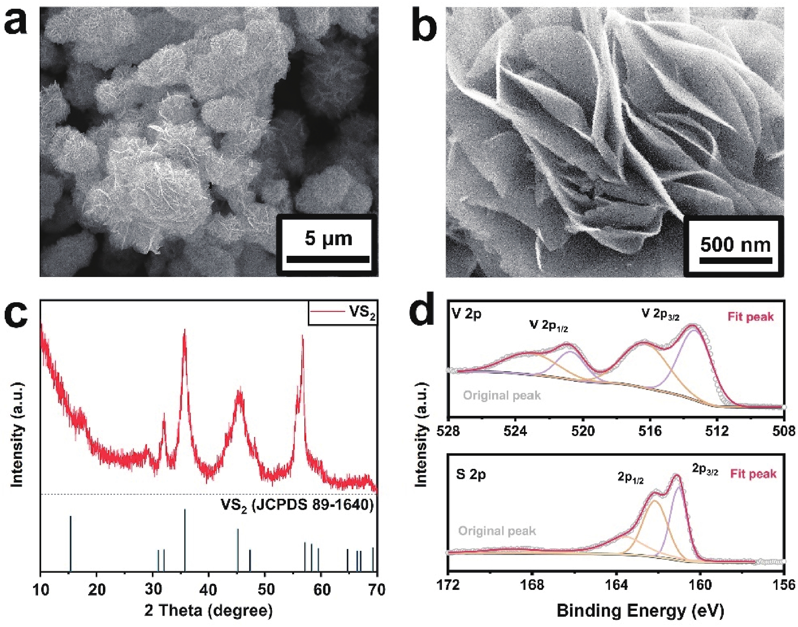
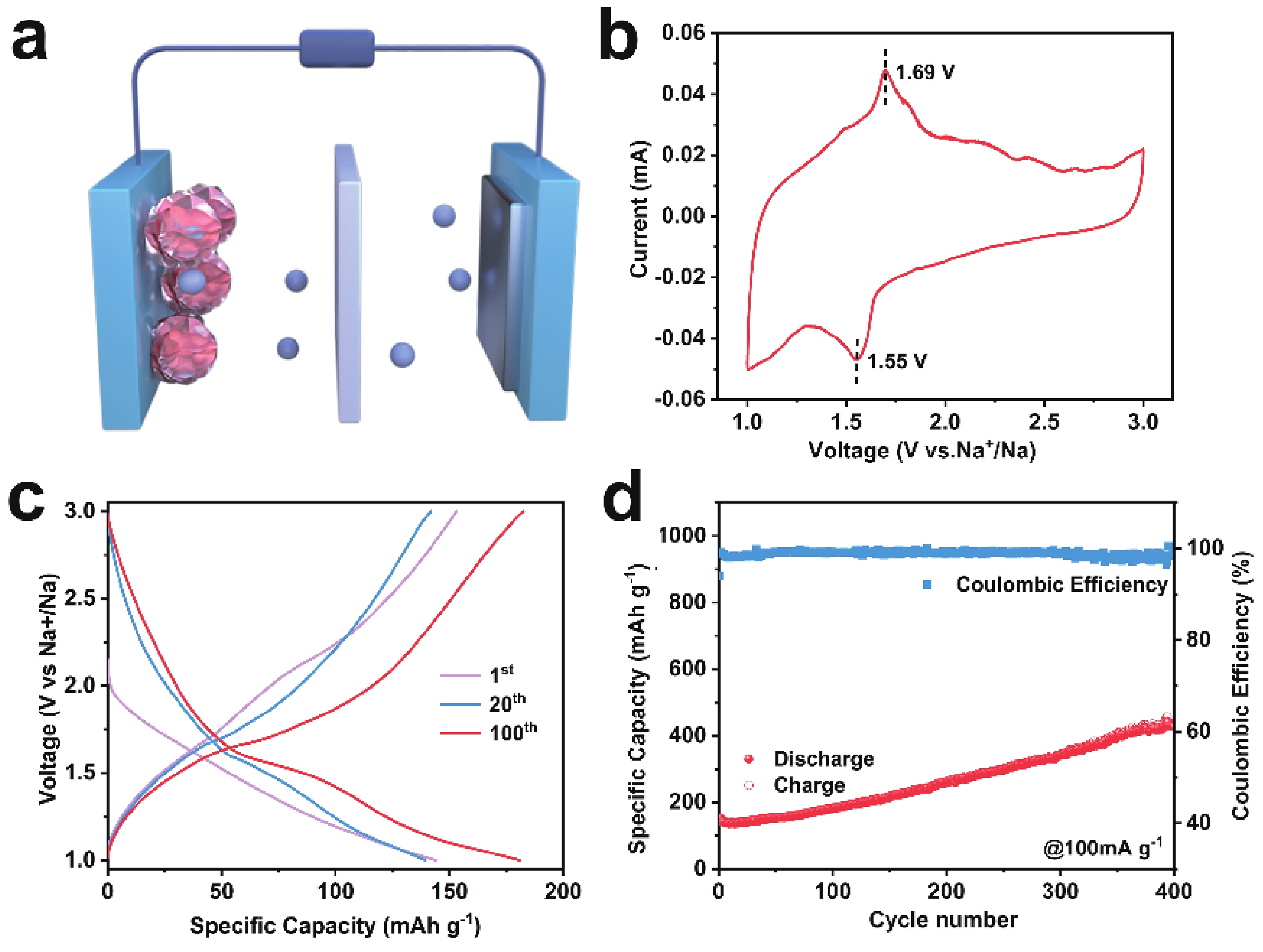
Metallic few-layered 1T phase vanadium disulfide nanosheets have been employed for boosting sodium ion batteries. It can deliver a capacity of 241 mAh∙g−1 at 100 mA∙g−1 after 200 cycles. Such long-term stability is attributed to the facile ion diffusion and electron transport resulting from the well-designed two-dimensional (2D) electron-electron correlations among V atoms in the 1T phase and optimized in-planar electric transport. Our results highlight the phase engineering into electrode design for energy storage.

J. Semicond.
2023, 44(11): 112801 doi: 10.1088/1674-4926/44/11/112801

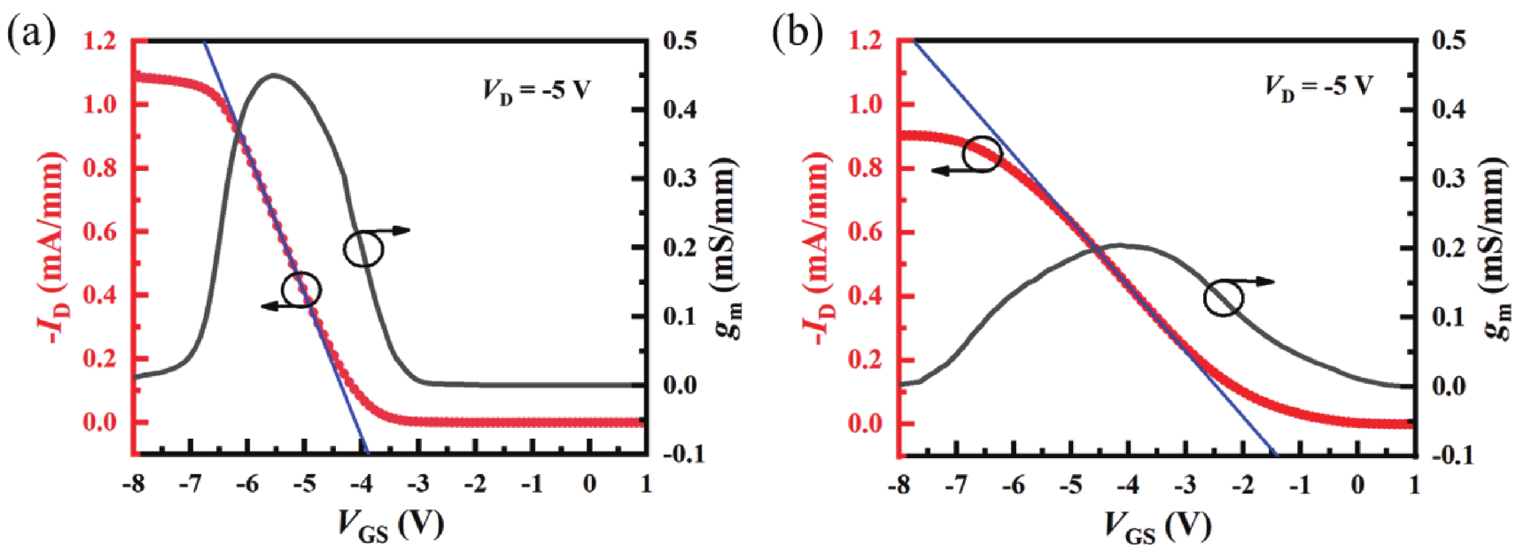
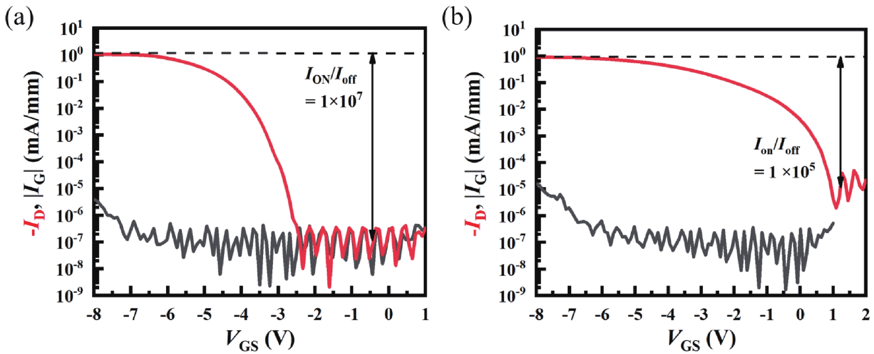
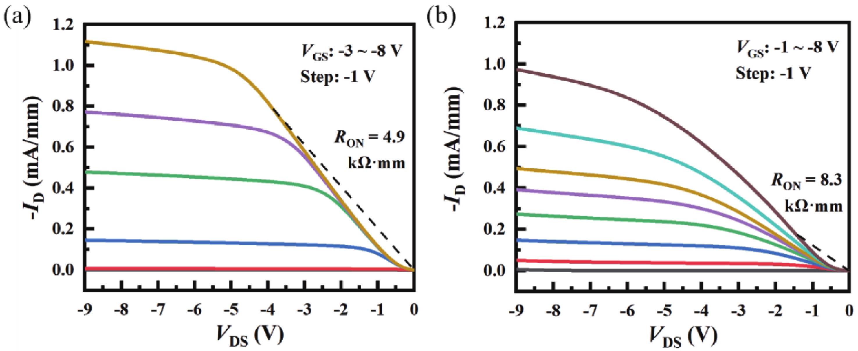
This letter showcases the successful fabrication of an enhancement-mode (E-mode) buried p-channel GaN field-effect-transistor on a standard p-GaN/AlGaN/GaN-on-Si power HEMT substrate. The transistor exhibits a threshold voltage (VTH) of −3.8 V, a maximum ON-state current (ION) of 1.12 mA/mm, and an impressive ION/IOFF ratio of 107. To achieve these remarkable results, an H plasma treatment was strategically applied to the gated p-GaN region, where a relatively thick GaN layer (i.e., 70 nm) was kept intact without aggressive gate recess. Through this treatment, the top portion of the GaN layer was converted to be hole-free, leaving only the bottom portion p-type and spatially separated from the etched GaN surface and gate-oxide/GaN interface. This approach allows for E-mode operation while retaining high-quality p-channel characteristics.


J. Semicond.
2023, 44(11): 114101 doi: 10.1088/1674-4926/44/11/114101
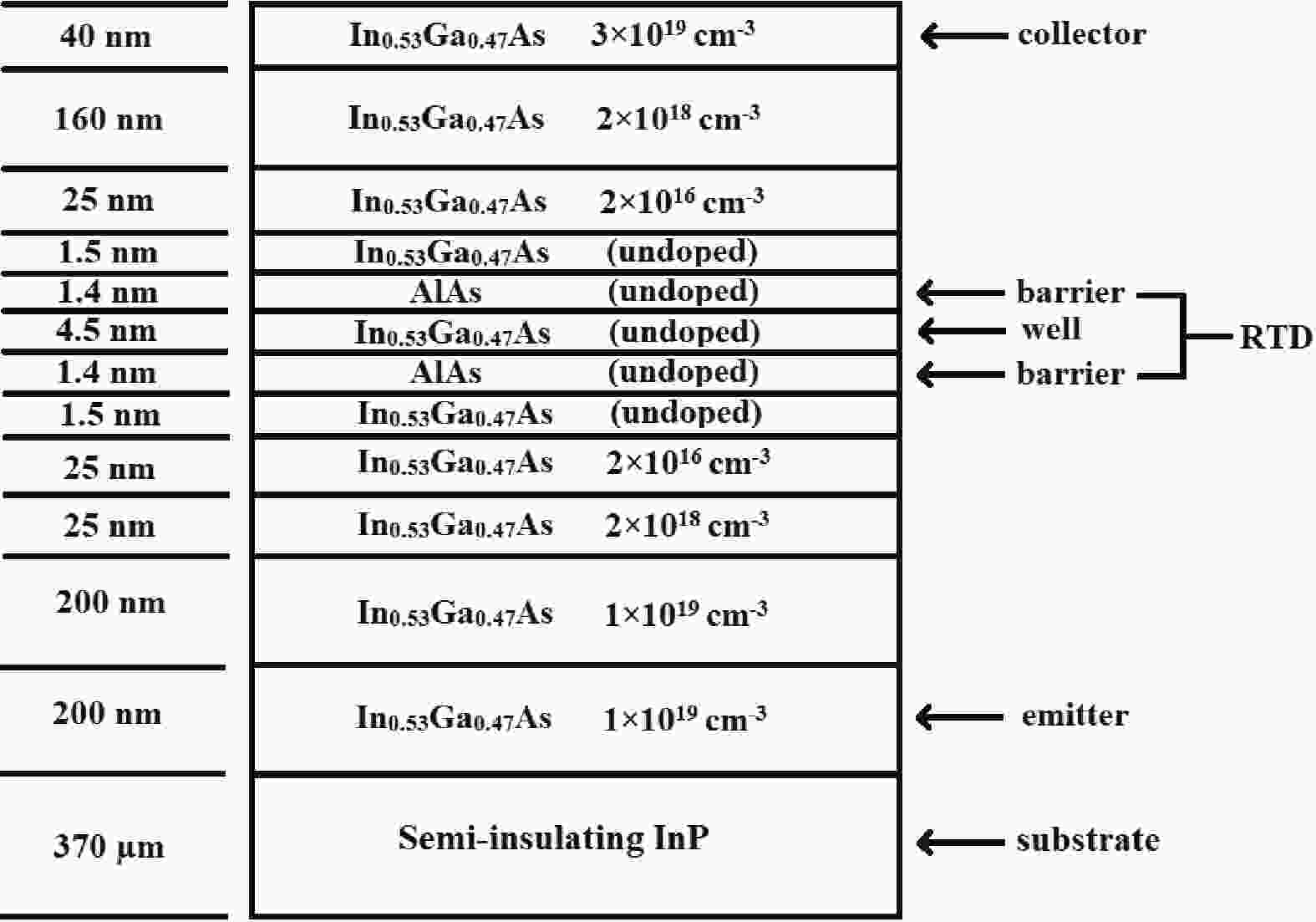
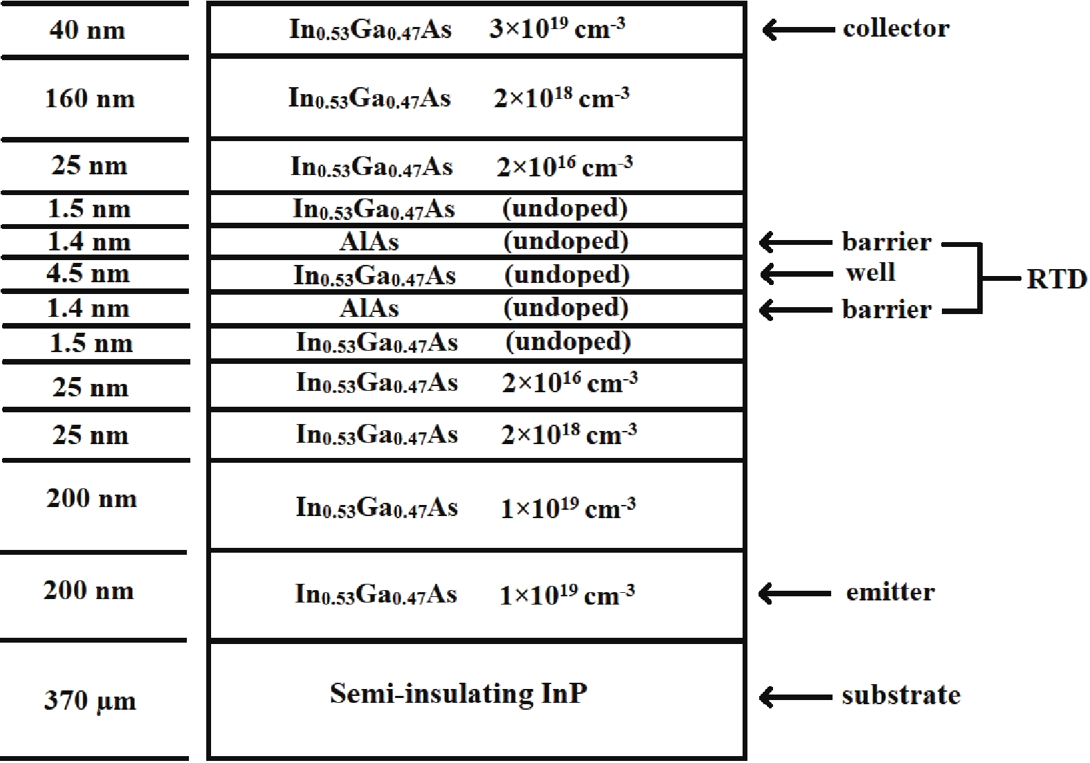
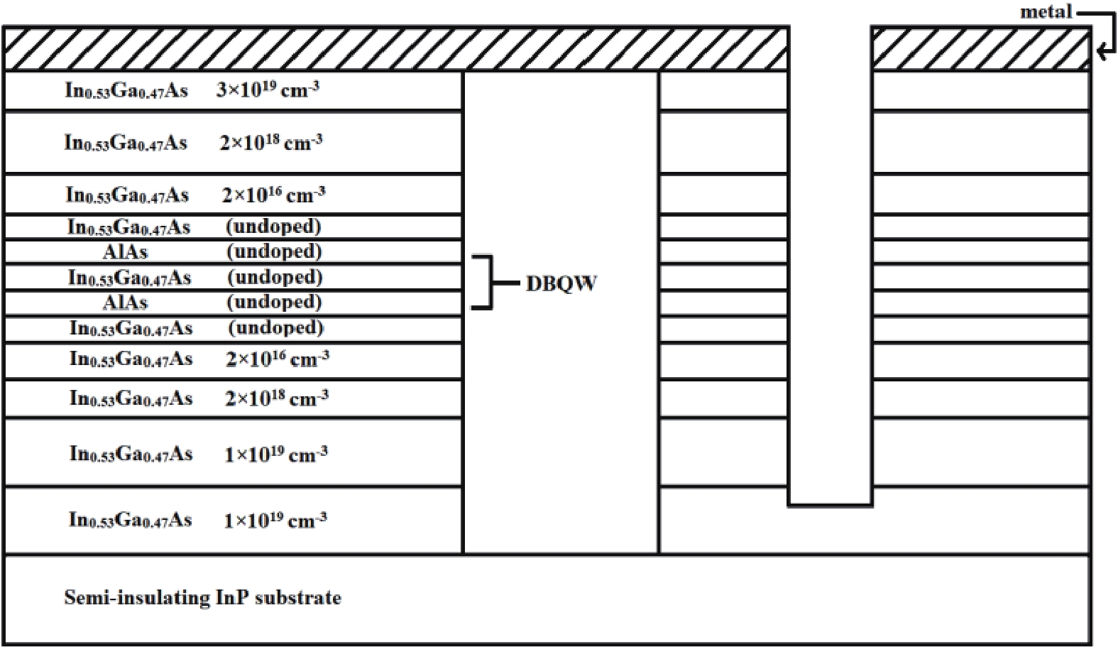
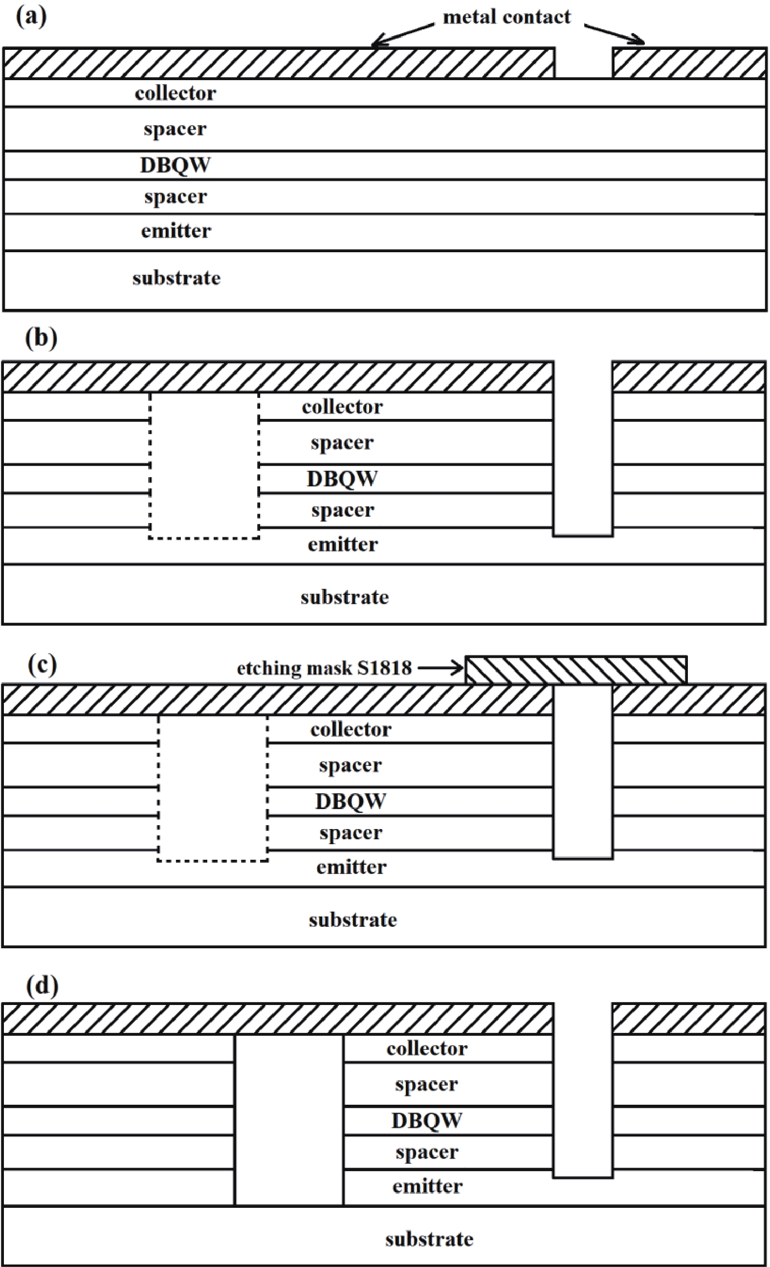
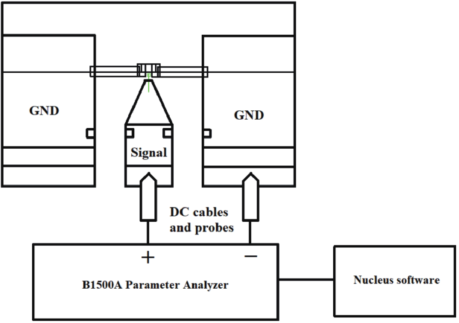
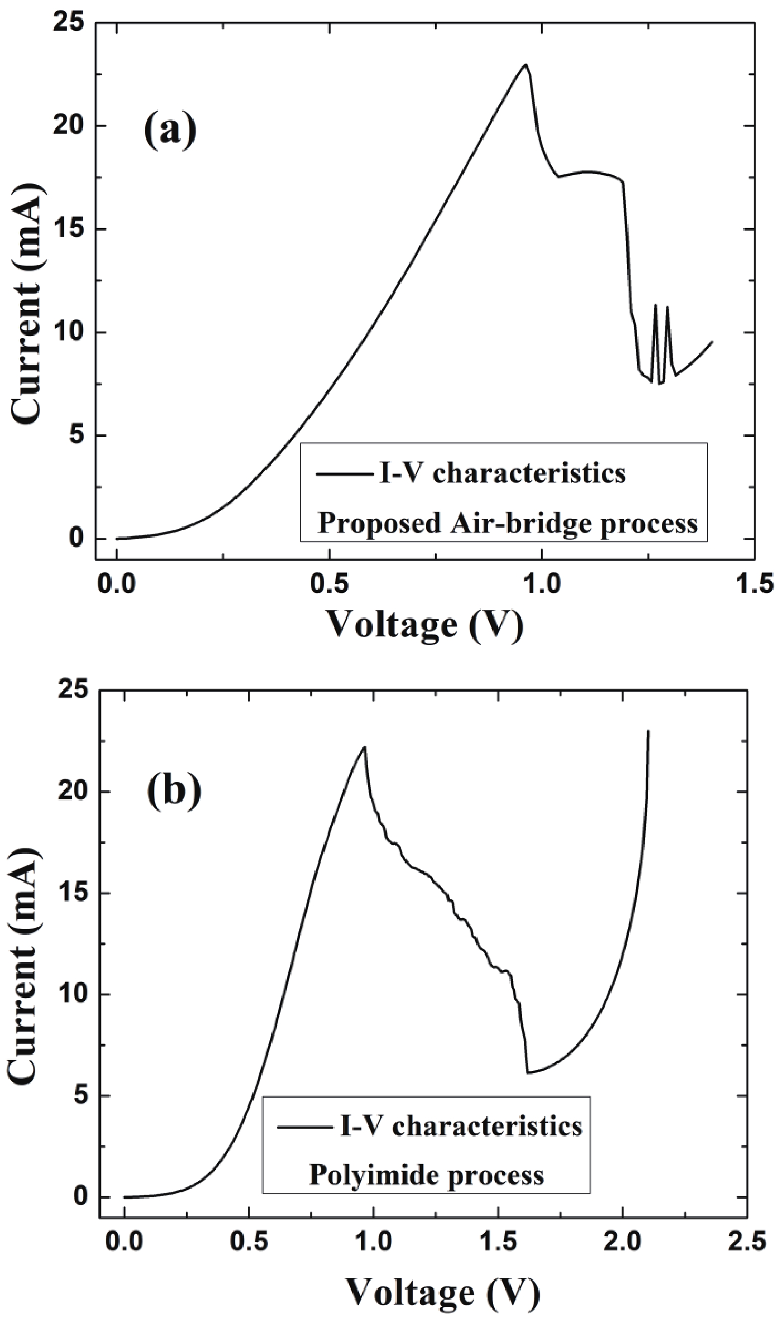
This article reports on the development of a simple two-step lithography process for double barrier quantum well (DBQW) InGaAs/AlAs resonant tunneling diode (RTD) on a semi-insulating indium phosphide (InP) substrate using an air-bridge technology. This approach minimizes processing steps, and therefore the processing time as well as the required resources. It is particularly suited for material qualification of new epitaxial layer designs. A DC performance comparison between the proposed process and the conventional process shows approximately the same results. We expect that this novel technique will aid in the recent and continuing rapid advances in RTD technology.

J. Semicond.
2023, 44(11): 114102 doi: 10.1088/1674-4926/44/11/114102
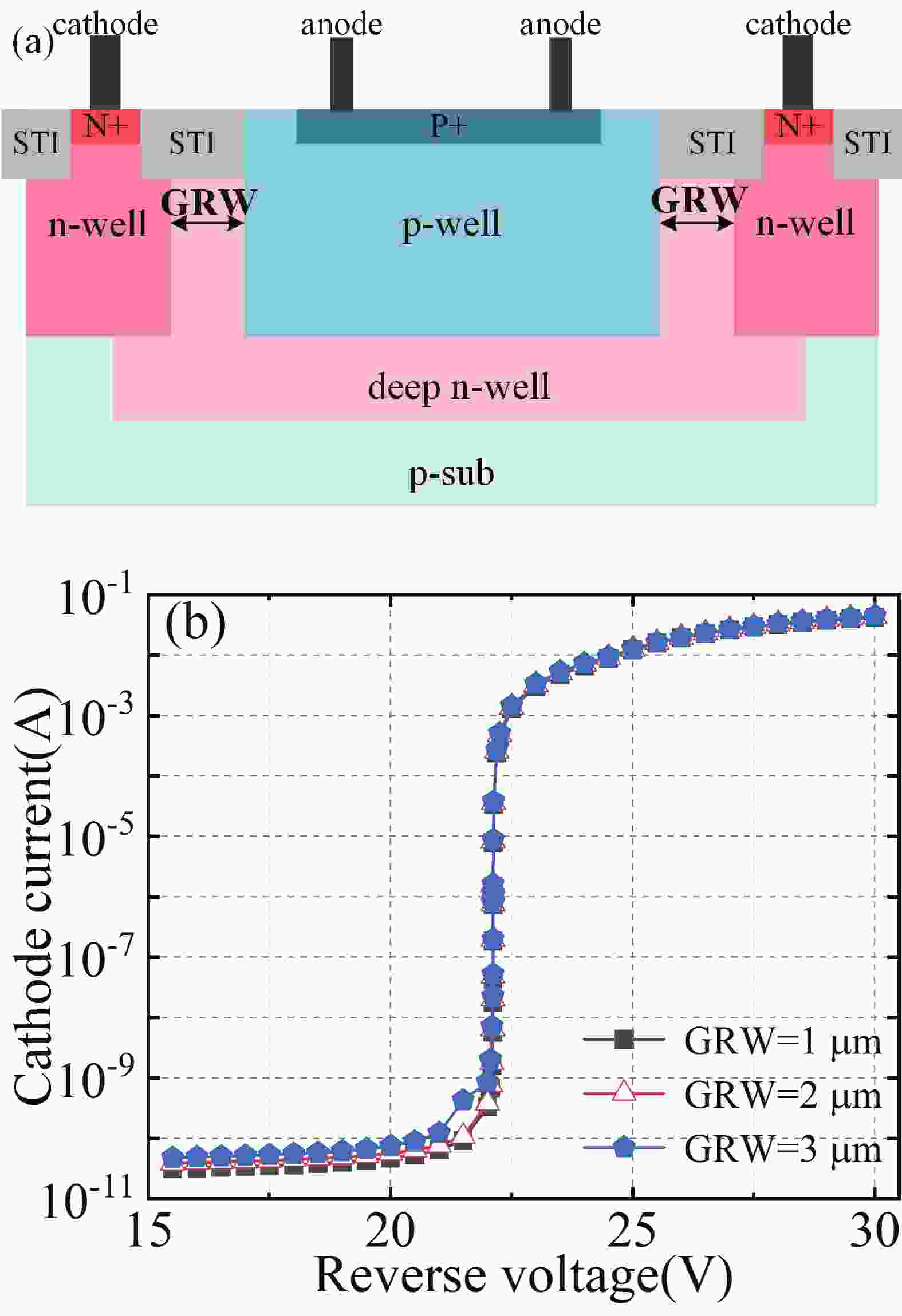
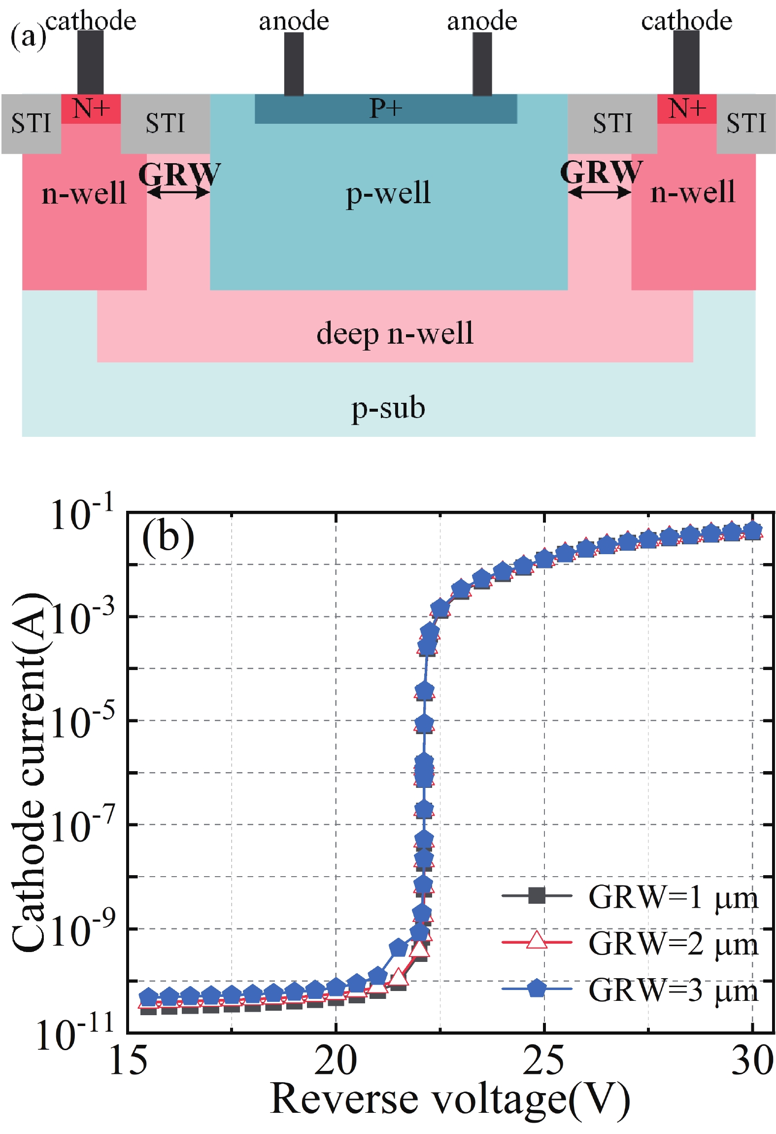
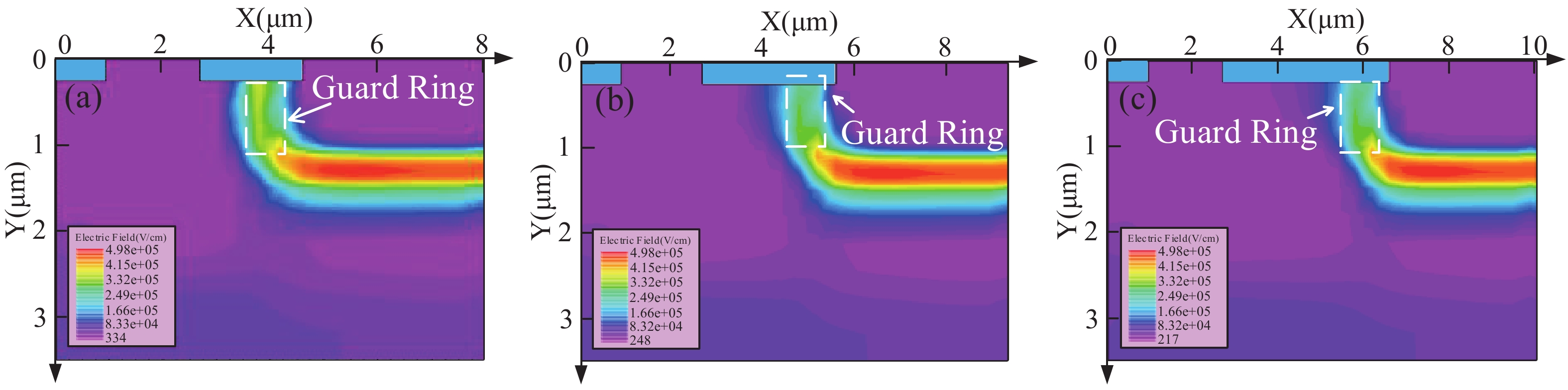
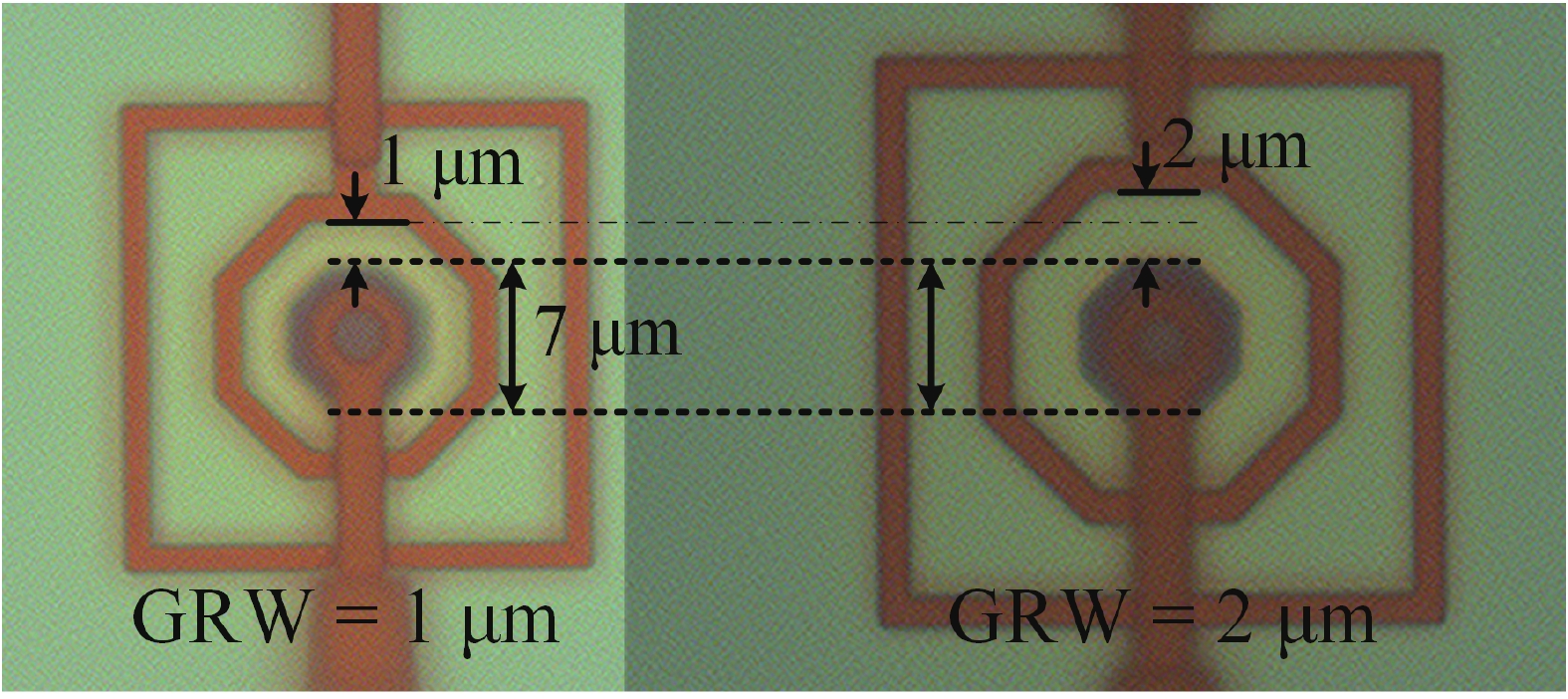
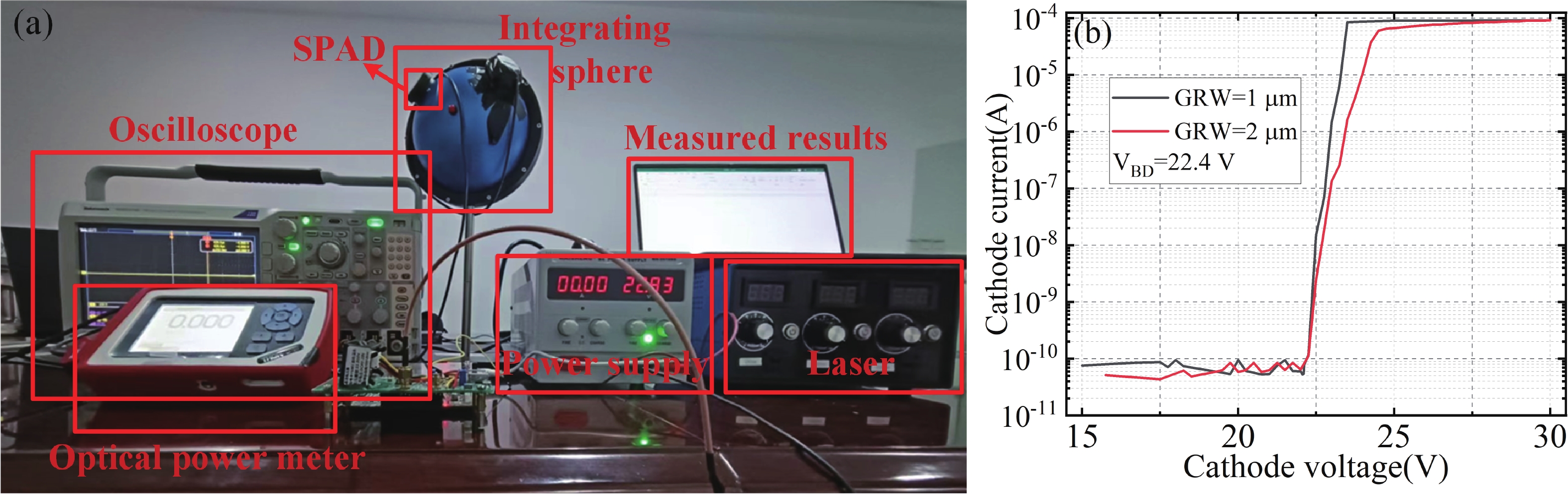
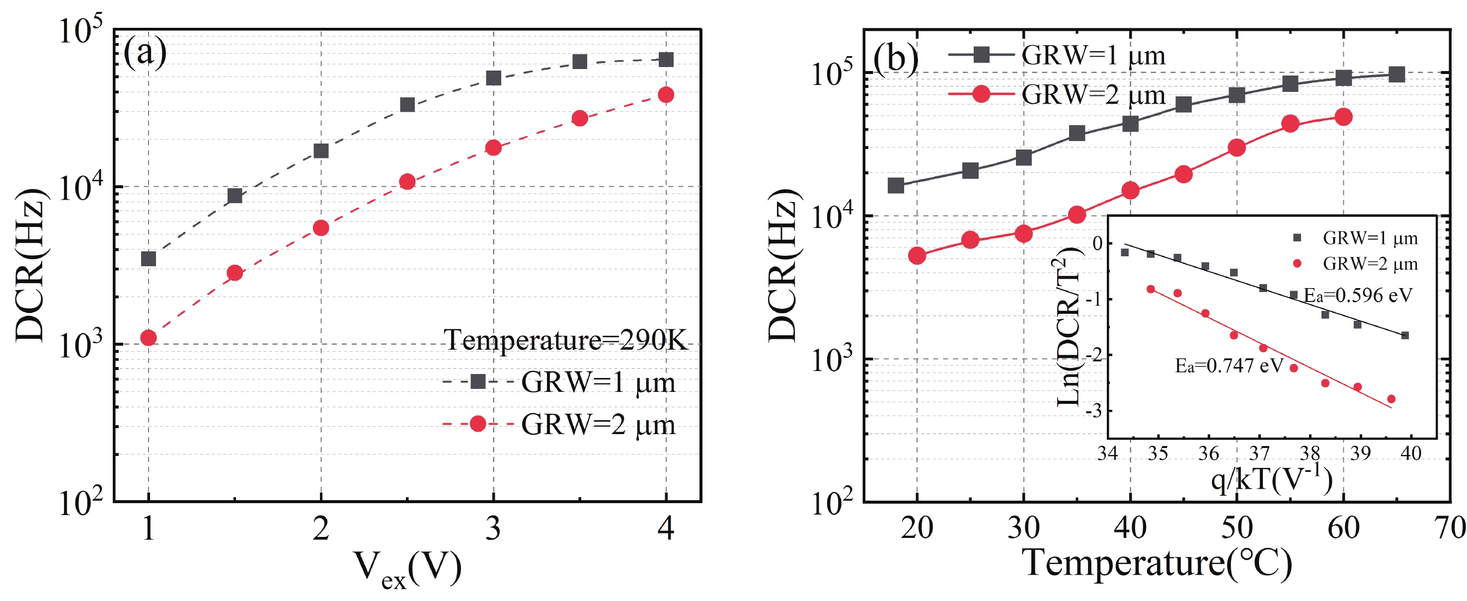
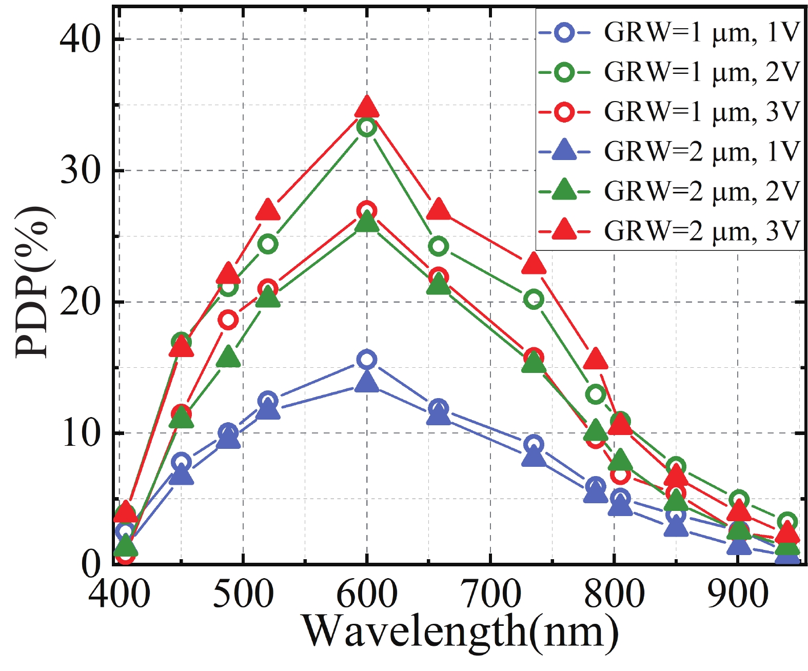
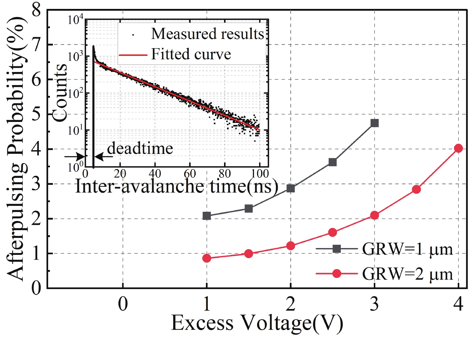
The influence of the virtual guard ring width (GRW) on the performance of the p-well/deep n-well single-photon avalanche diode (SPAD) in a 180 nm standard CMOS process was investigated. TCAD simulation demonstrates that the electric field strength and current density in the guard ring are obviously enhanced when GRW is decreased to 1 μm. It is experimentally found that, compared with an SPAD with GRW = 2 μm, the dark count rate (DCR) and afterpulsing probability (AP) of the SPAD with GRW = 1 μm is significantly increased by 2.7 times and twofold, respectively, meanwhile, its photon detection probability (PDP) is saturated and hard to be promoted at over 2 V excess bias voltage. Although the fill factor (FF) can be enlarged by reducing GRW, the dark noise of devices is negatively affected due to the enhanced trap-assisted tunneling (TAT) effect in the 1 μm guard ring region. By comparison, the SPAD with GRW = 2 μm can achieve a better trade-off between the FF and noise performance. Our study provides a design guideline for guard rings to realize a low-noise SPAD for large-array applications.

J. Semicond.
2023, 44(11): 114103 doi: 10.1088/1674-4926/44/11/114103

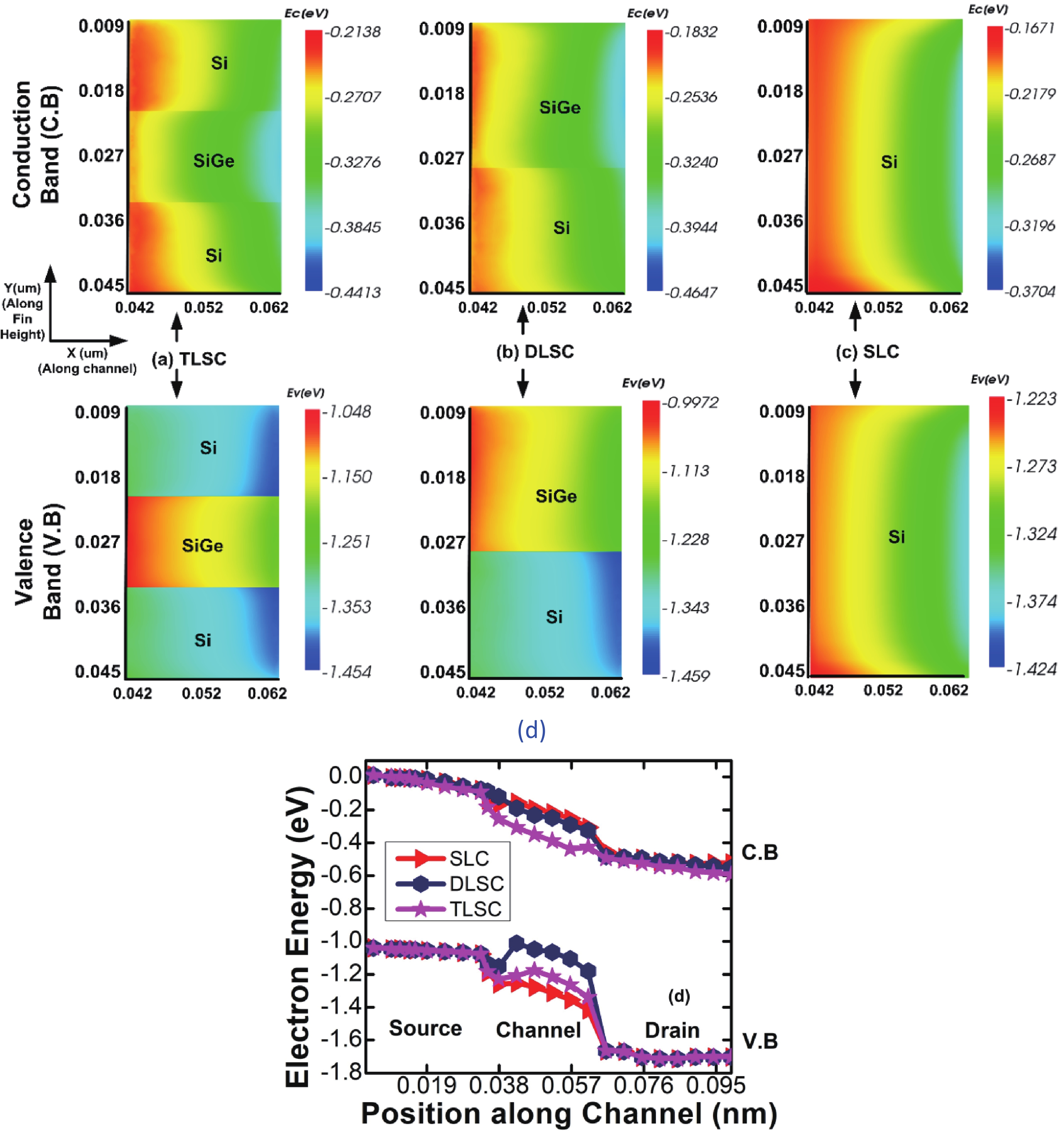
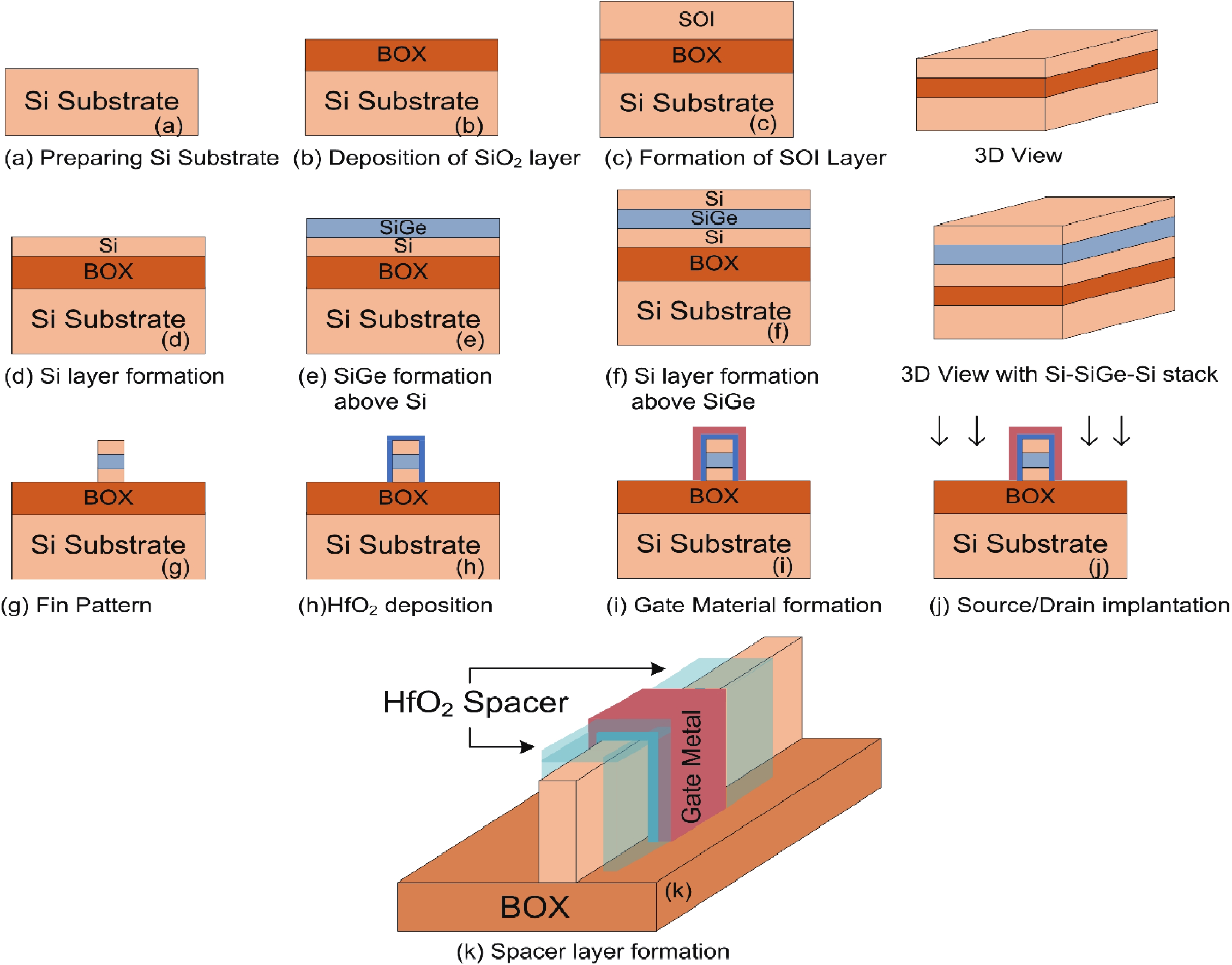
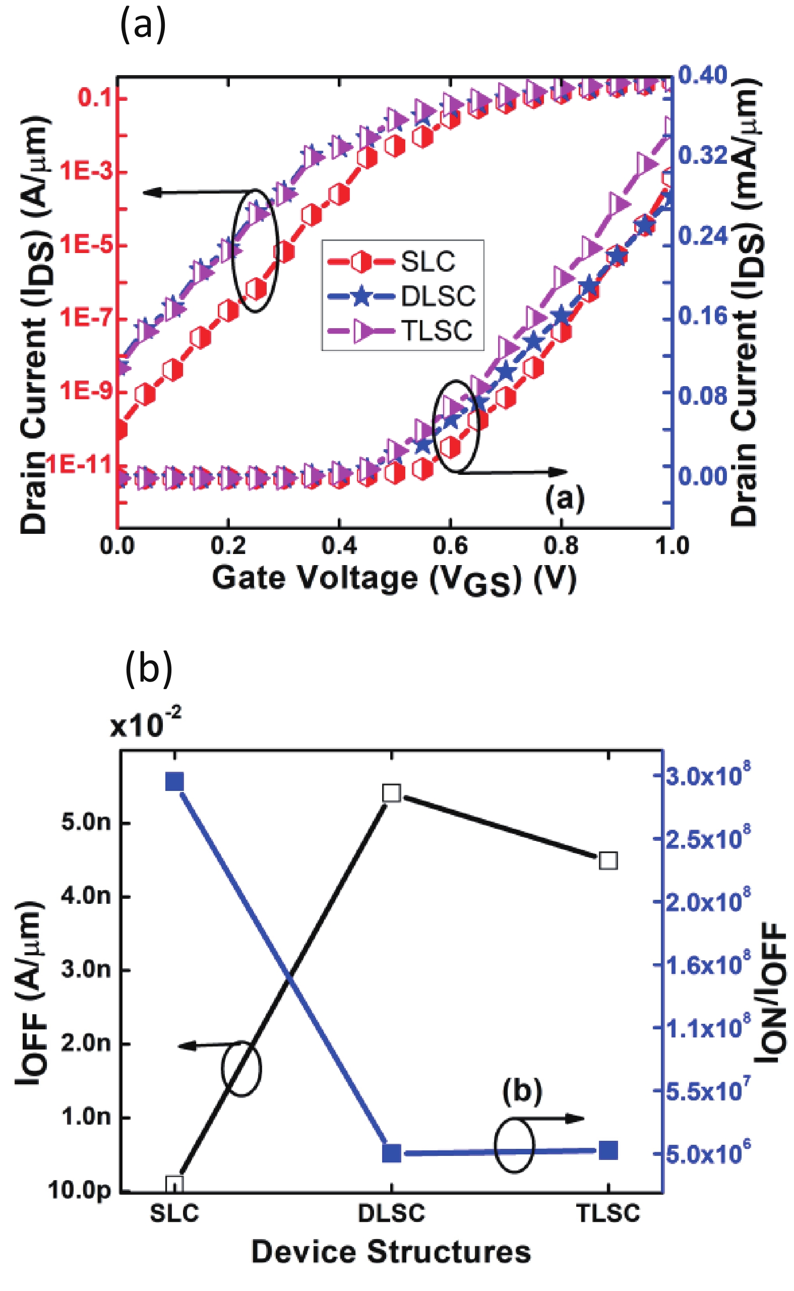
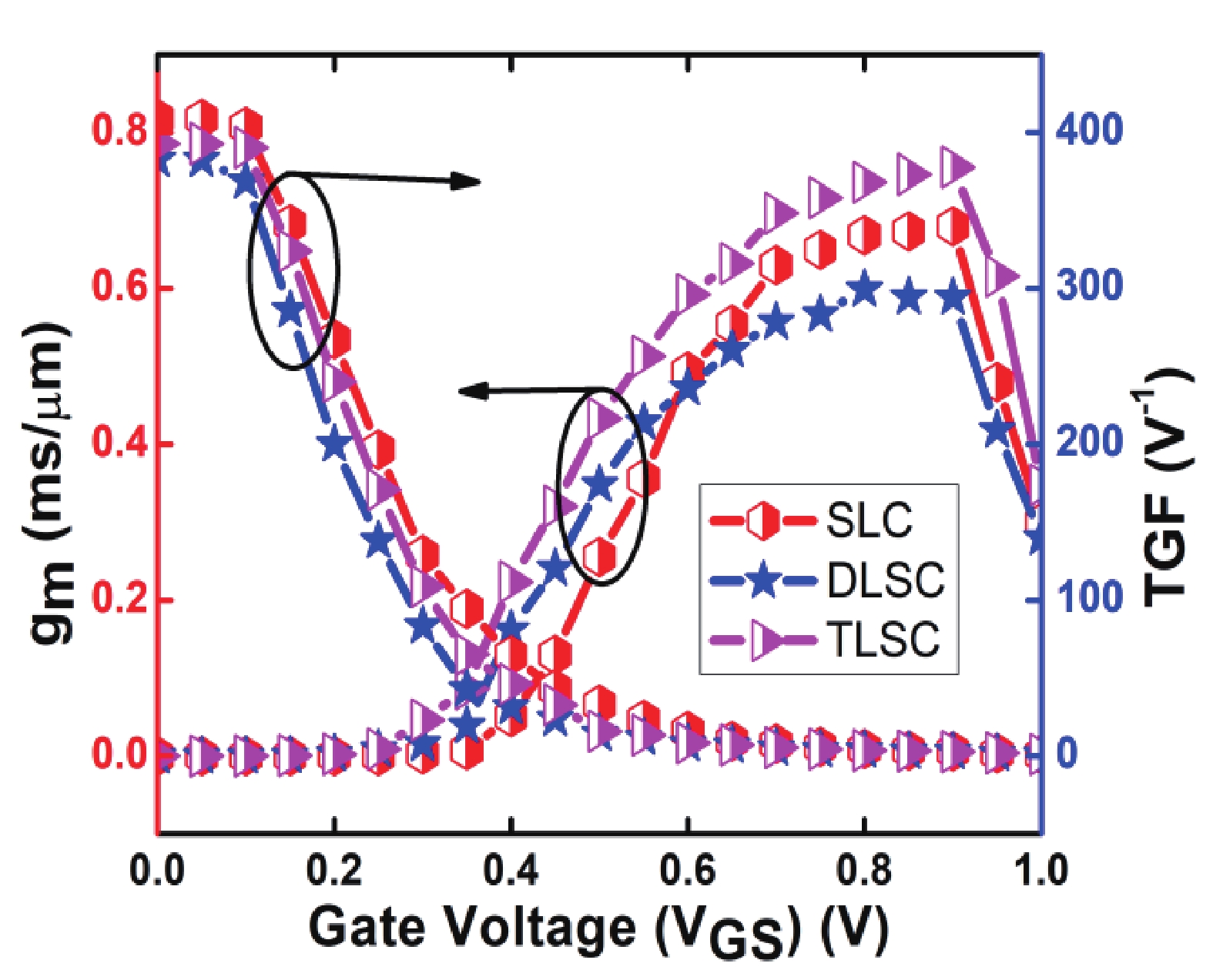
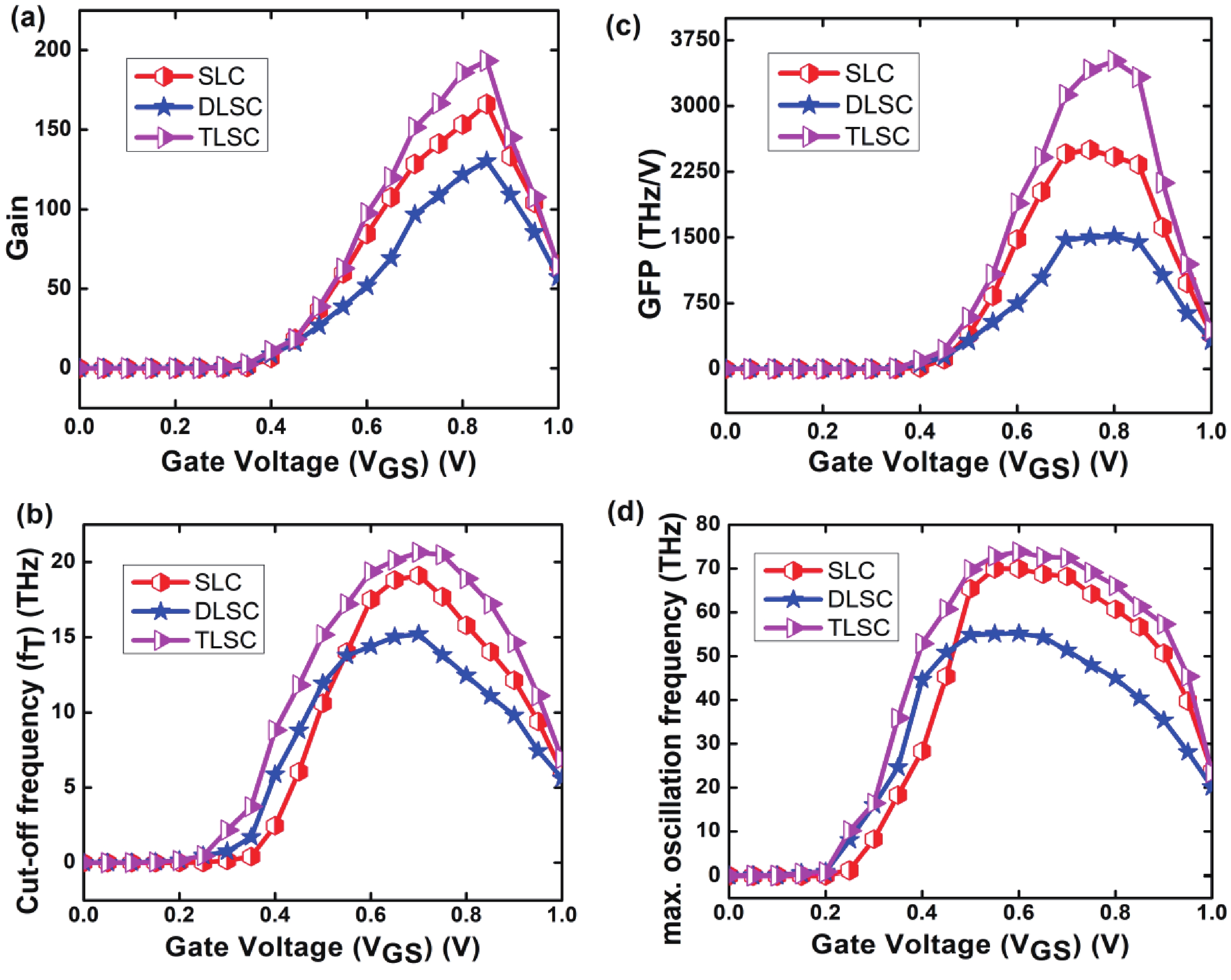
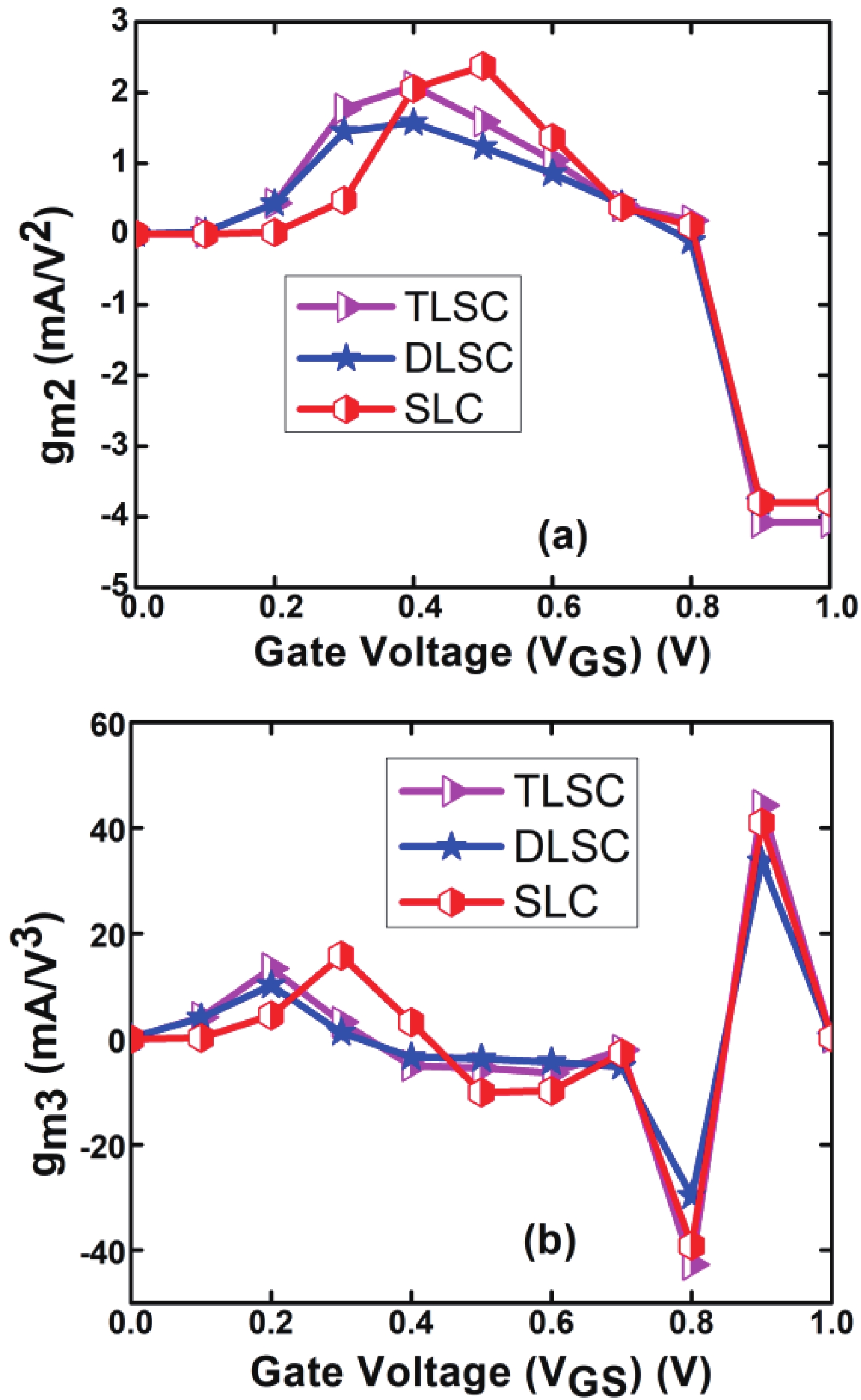
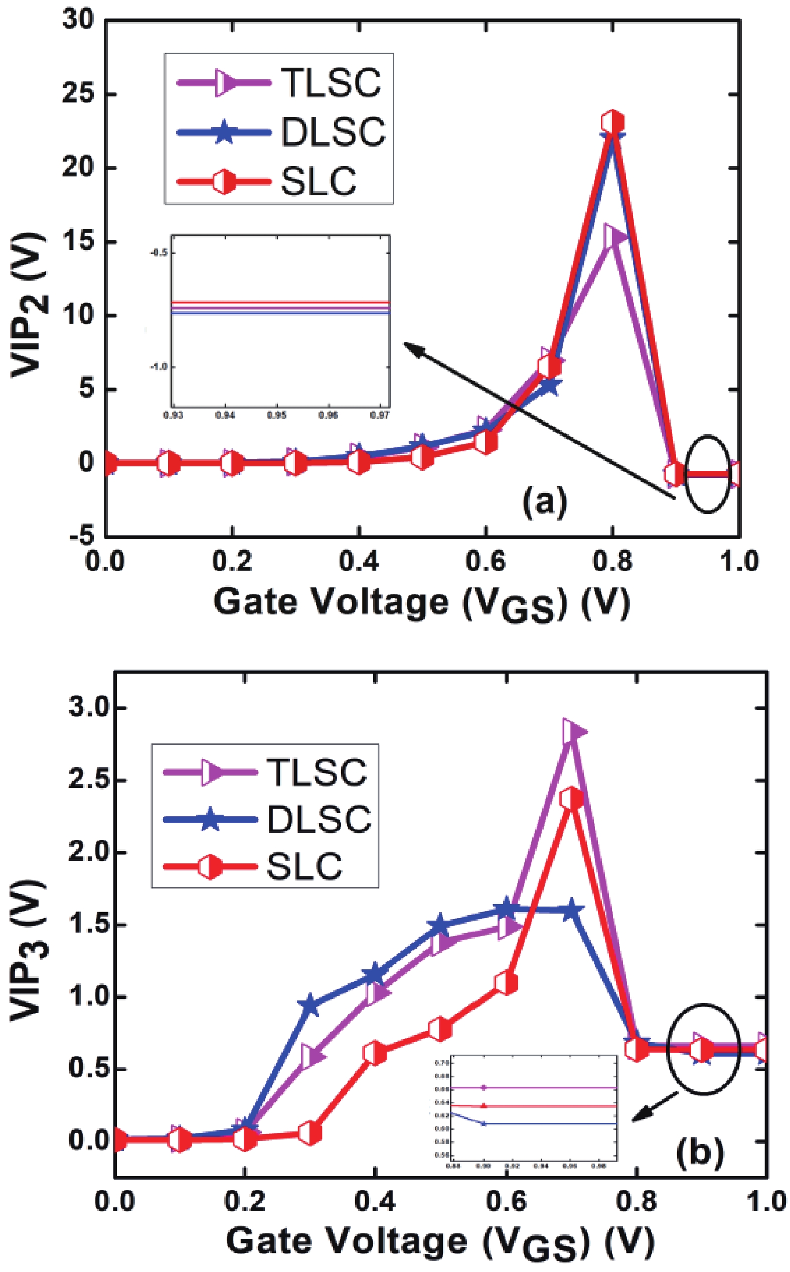
This manuscript explores the behavior of a junctionless tri-gate FinFET at the nano-scale region using SiGe material for the channel. For the analysis, three different channel structures are used: (a) tri-layer stack channel (TLSC) (Si–SiGe–Si), (b) double layer stack channel (DLSC) (SiGe–Si), (c) single layer channel (SLC) (Si). The I−V characteristics, subthreshold swing (SS), drain-induced barrier lowering (DIBL), threshold voltage (Vt), drain current (ION), OFF current (IOFF), and ON-OFF current ratio (ION/IOFF) are observed for the structures at a 20 nm gate length. It is seen that TLSC provides 21.3% and 14.3% more ON current than DLSC and SLC, respectively. The paper also explores the analog and RF factors such as input transconductance (gm), output transconductance (gds), gain (gm/gds), transconductance generation factor (TGF), cut-off frequency (fT), maximum oscillation frequency (fmax), gain frequency product (GFP) and linearity performance parameters such as second and third-order harmonics (gm2, gm3), voltage intercept points (VIP2, VIP3) and 1-dB compression points for the three structures. The results show that the TLSC has a high analog performance due to more gm and provides 16.3%, 48.4% more gain than SLC and DLSC, respectively and it also provides better linearity. All the results are obtained using the VisualTCAD tool.


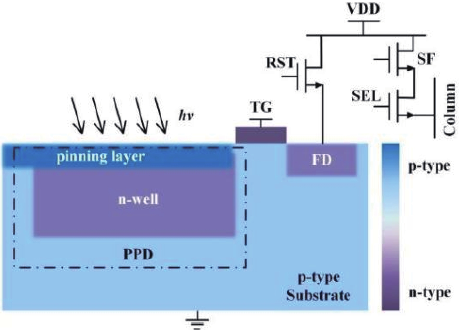
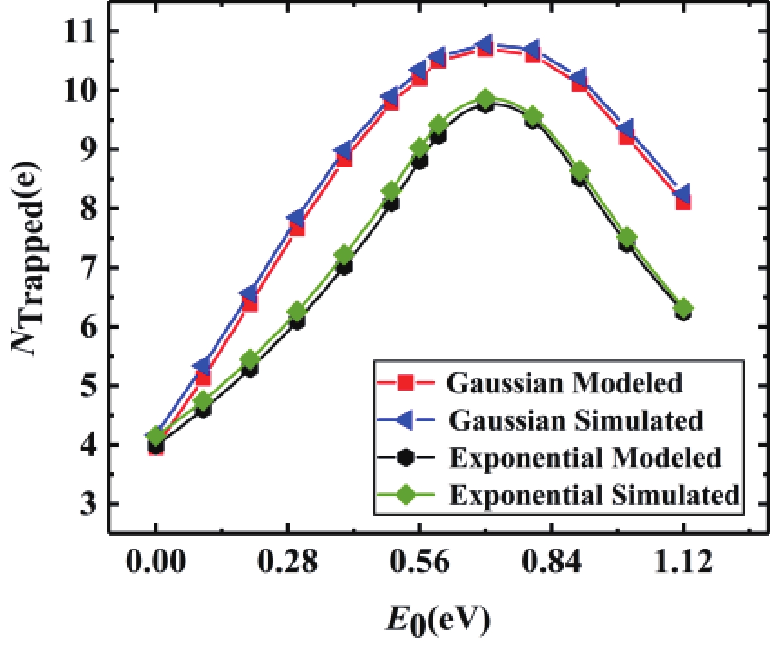
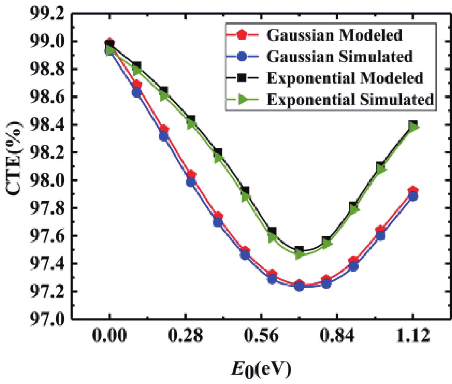
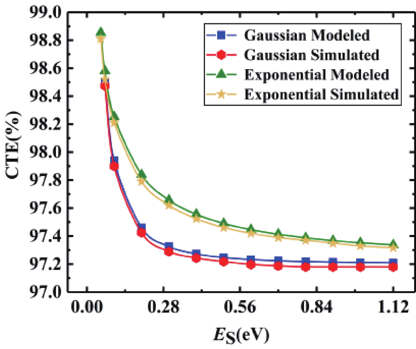
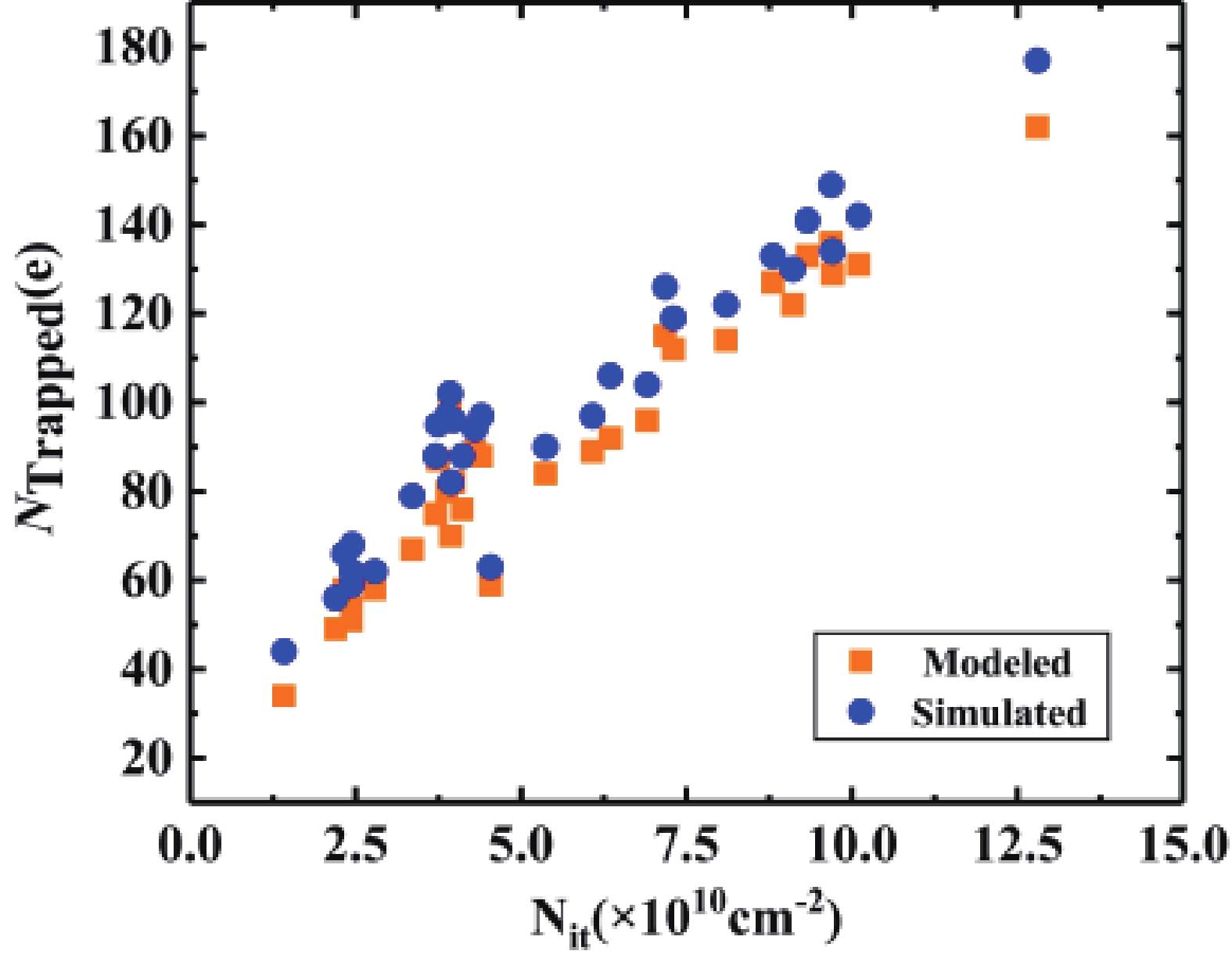
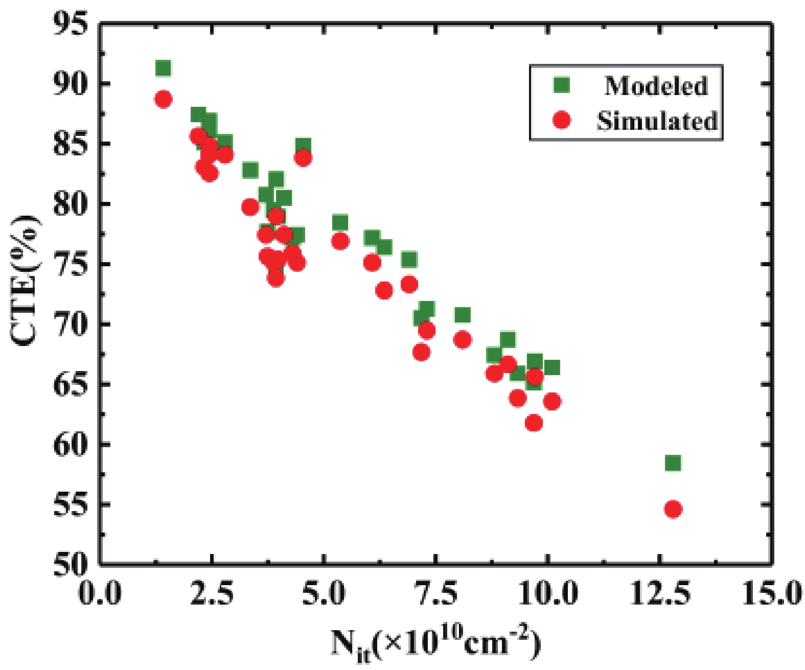
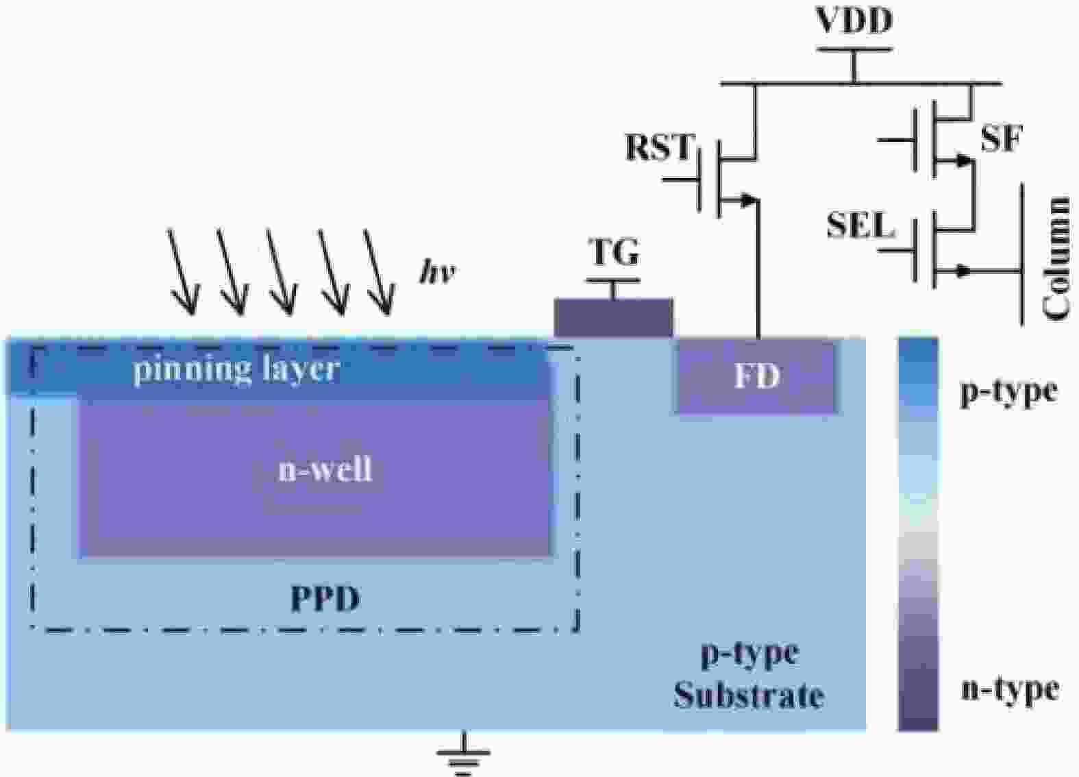
Incomplete charge transfer in CMOS image sensor caused by Si/SiO2 interface states in the TG channel
J. Semicond.
2023, 44(11): 114104 doi: 10.1088/1674-4926/44/11/114104
CMOS image sensors produced by the existing CMOS manufacturing process usually have difficulty achieving complete charge transfer owing to the introduction of potential barriers or Si/SiO2 interface state traps in the charge transfer path, which reduces the charge transfer efficiency and image quality. Until now, scholars have only considered mechanisms that limit charge transfer from the perspectives of potential barriers and spill back effect under high illumination condition. However, the existing models have thus far ignored the charge transfer limitation due to Si/SiO2 interface state traps in the transfer gate channel, particularly under low illumination. Therefore, this paper proposes, for the first time, an analytical model for quantifying the incomplete charge transfer caused by Si/SiO2 interface state traps in the transfer gate channel under low illumination. This model can predict the variation rules of the number of untransferred charges and charge transfer efficiency when the trap energy level follows Gaussian distribution, exponential distribution and measured distribution. The model was verified with technology computer-aided design simulations, and the results showed that the simulation results exhibit the consistency with the proposed model.