Issue Browser
Volume 44, Issue 4,
Apr 2023
J. Semicond.
2023, 44(4): 041101 doi: 10.1088/1674-4926/44/4/041101
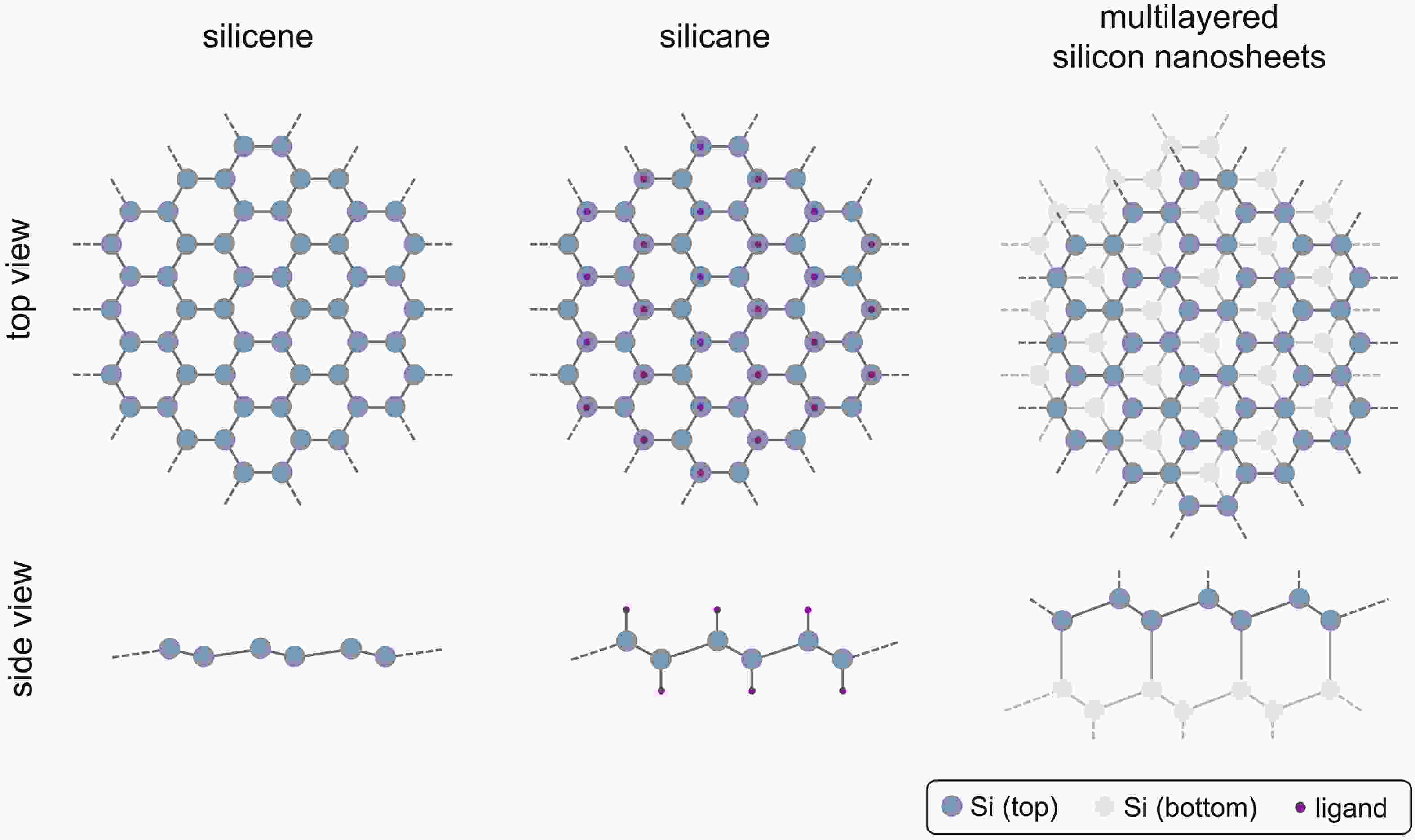
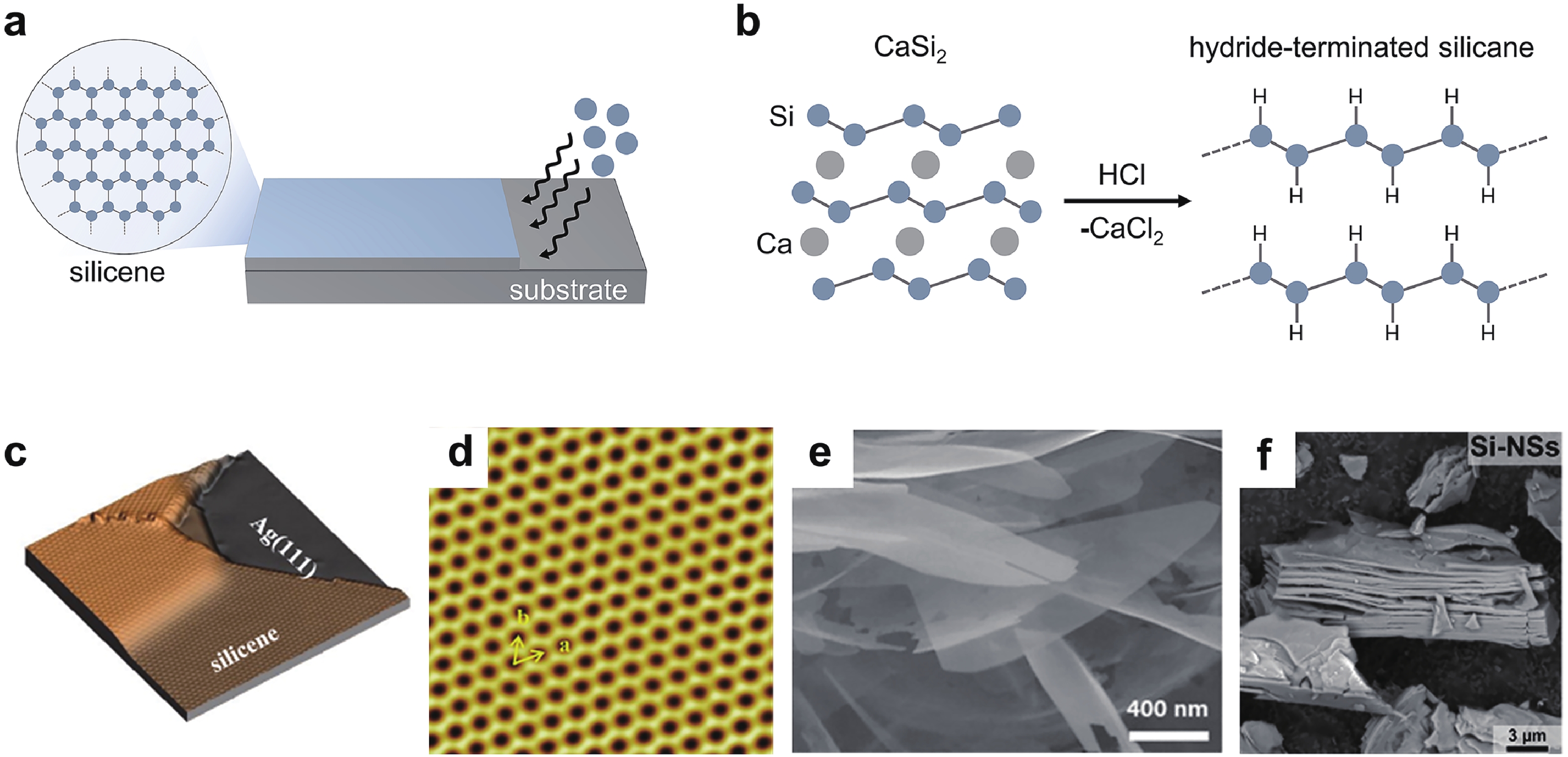
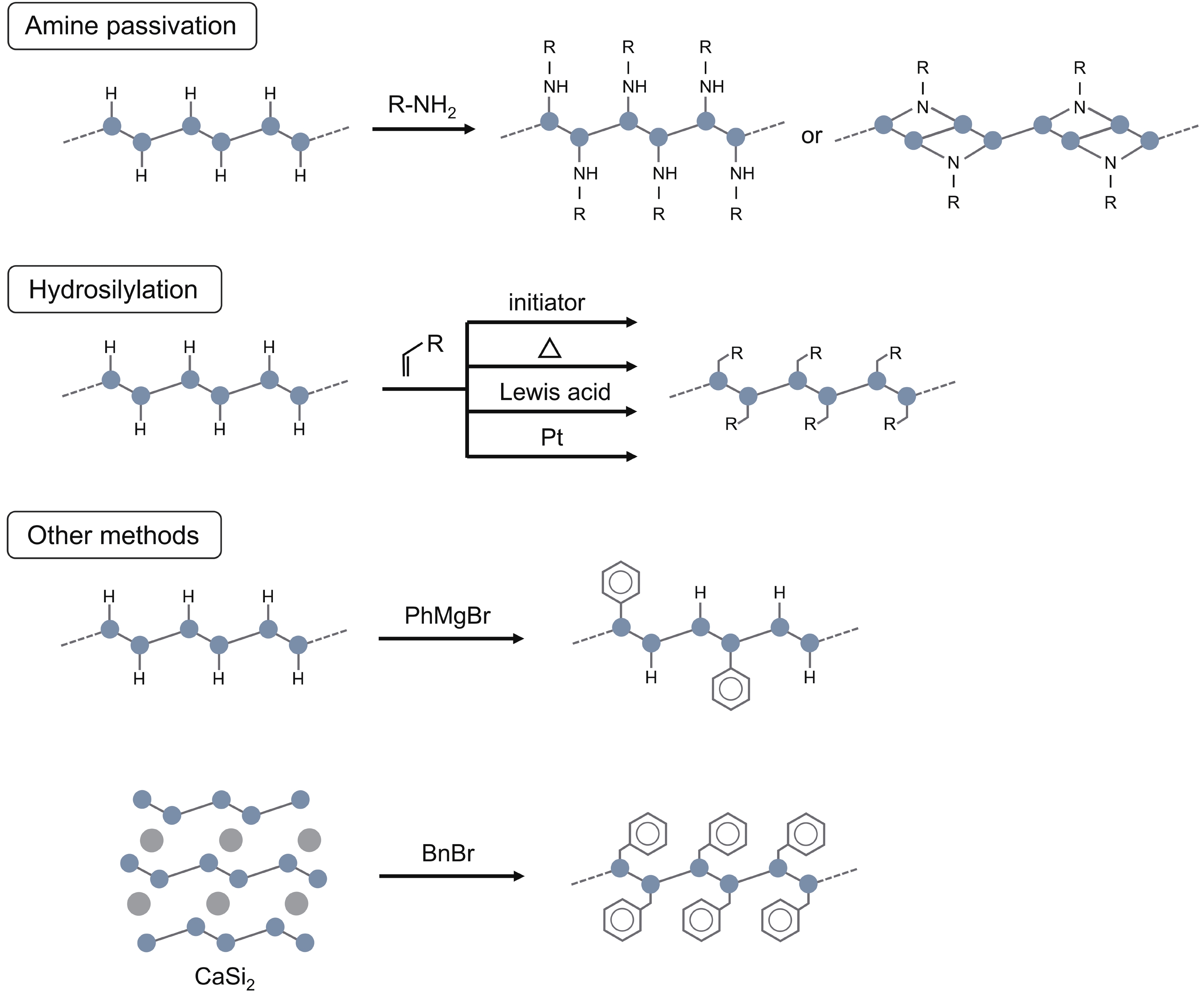
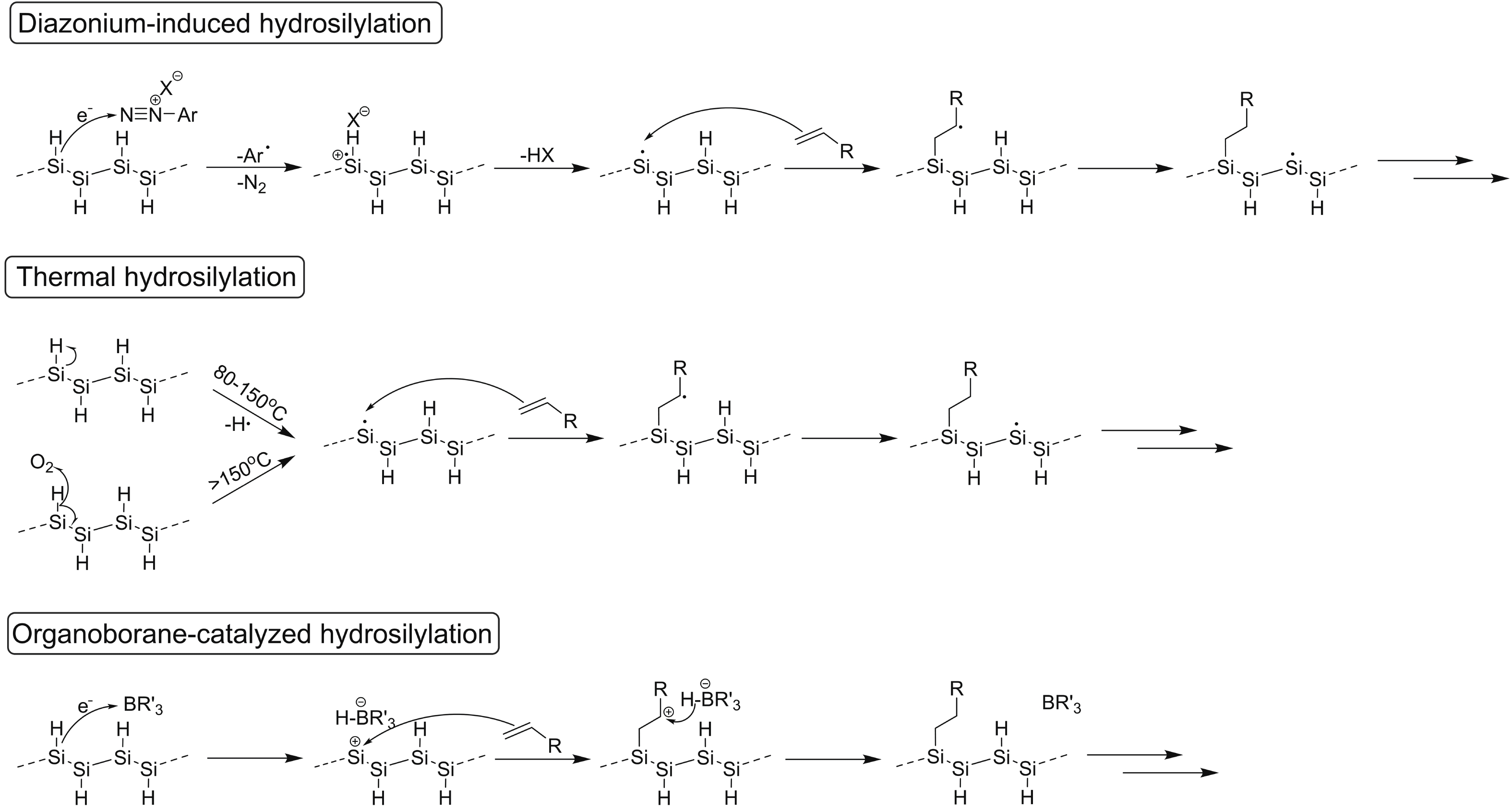
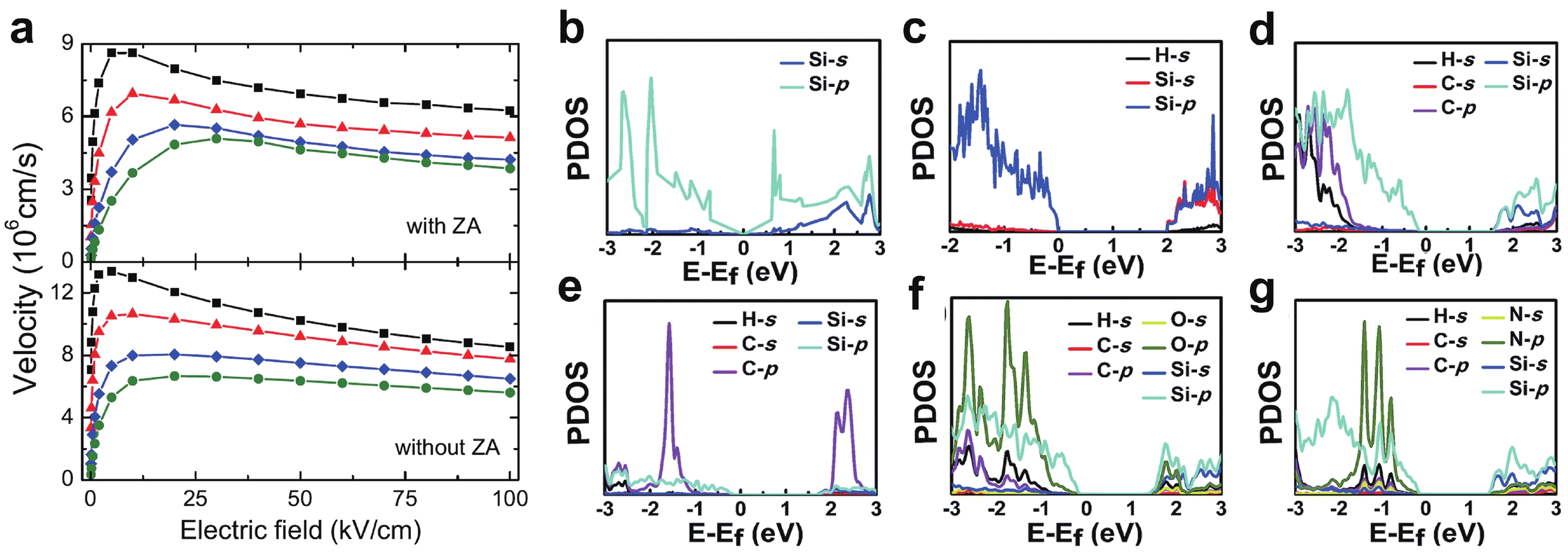
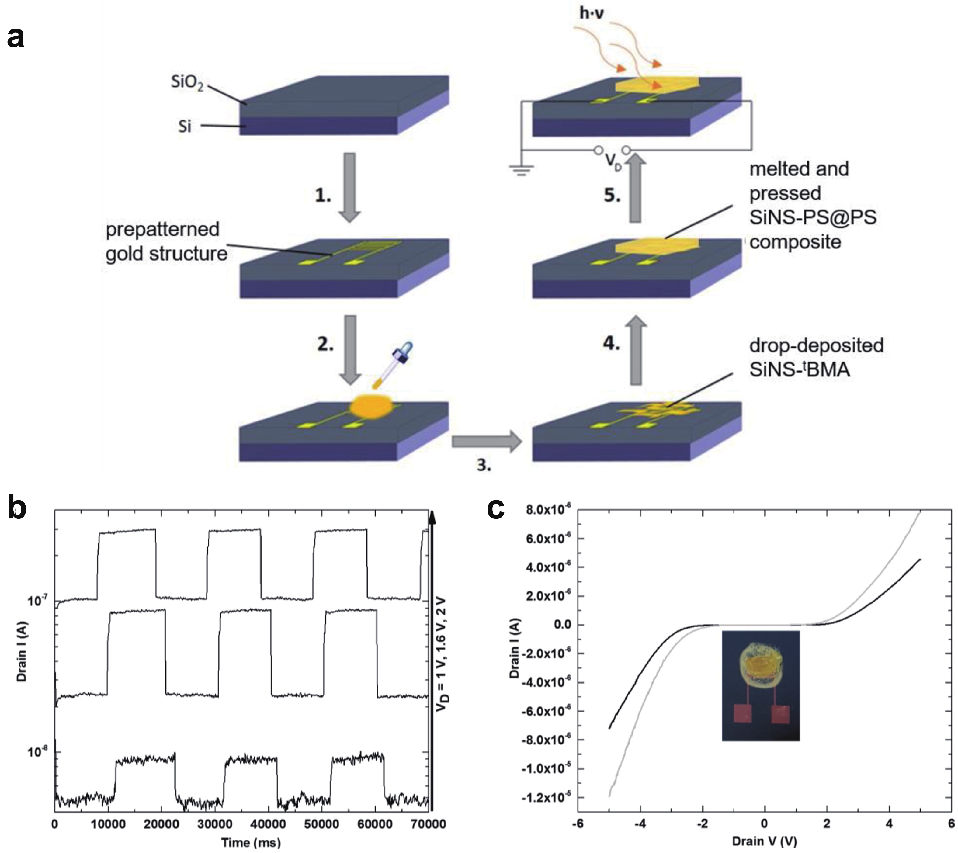
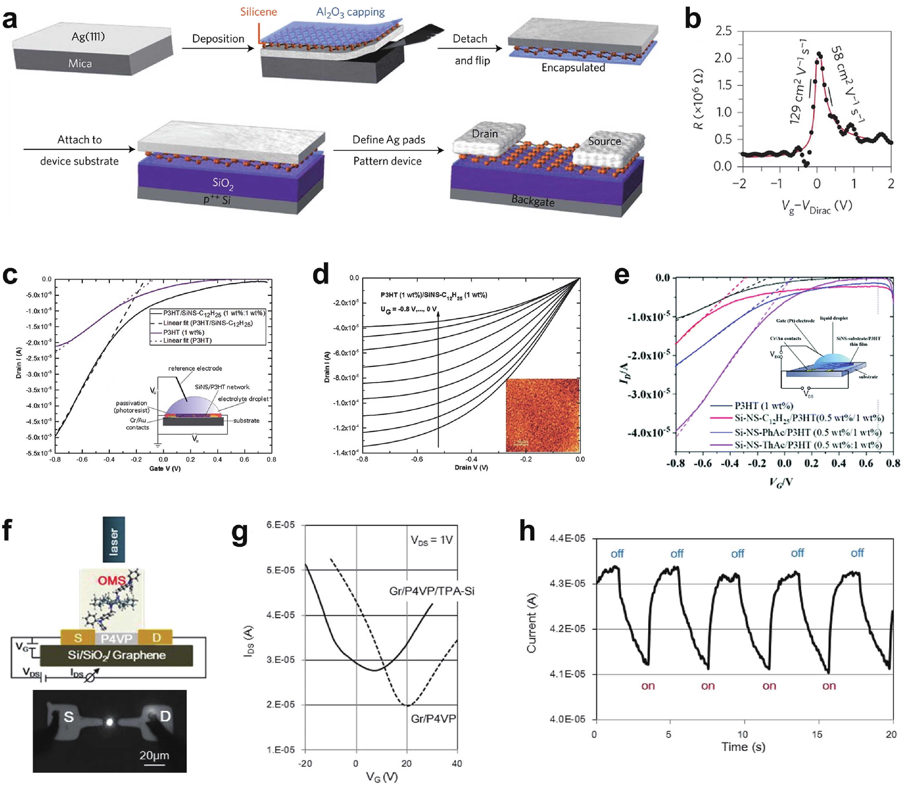
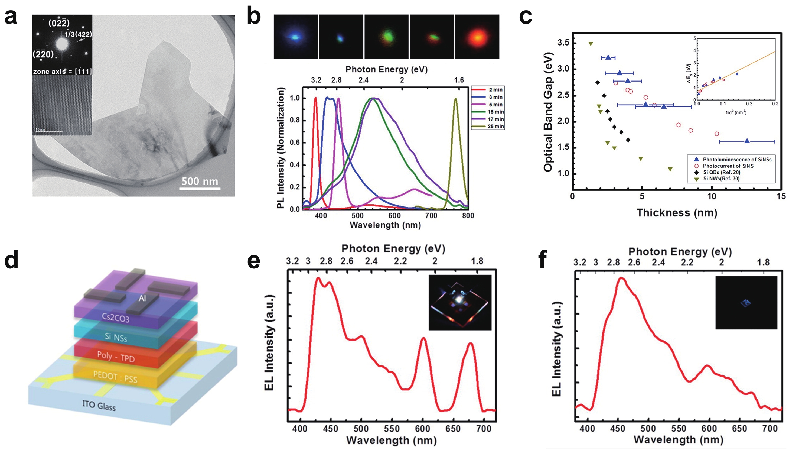
Silicon nanomaterials have been of immense interest in the last few decades due to their remarkable optoelectronic responses, elemental abundance, and higher biocompatibility. Two-dimensional silicon is one of the new allotropes of silicon and has many compelling properties such as quantum-confined photoluminescence, high charge carrier mobilities, anisotropic electronic and magnetic response, and non-linear optical properties. This review summarizes the recent advances in the synthesis of two-dimensional silicon nanomaterials with a range of structures (silicene, silicane, and multilayered silicon), surface ligand engineering, and corresponding optoelectronic applications.


J. Semicond.
2023, 44(4): 041601 doi: 10.1088/1674-4926/44/4/041601
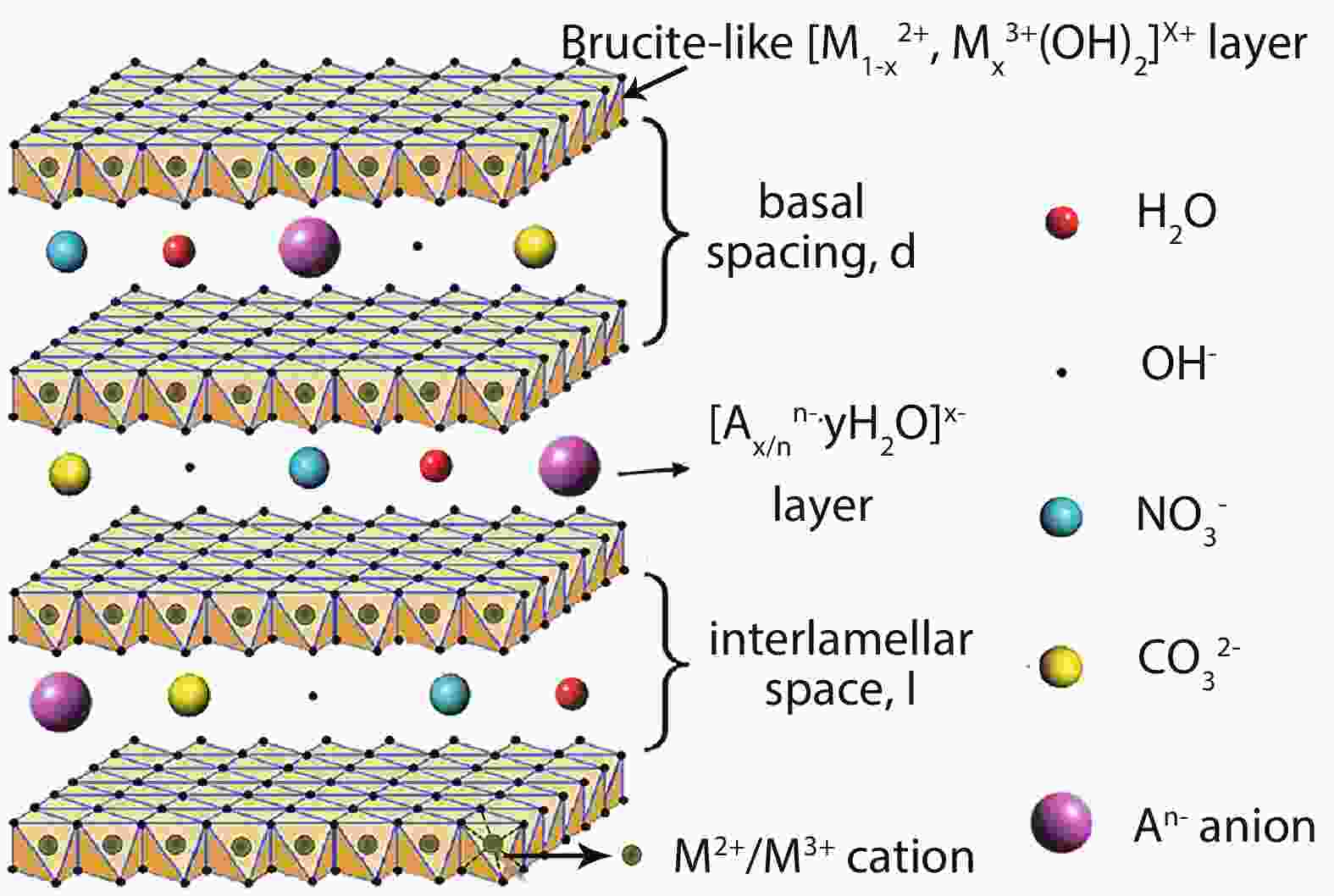
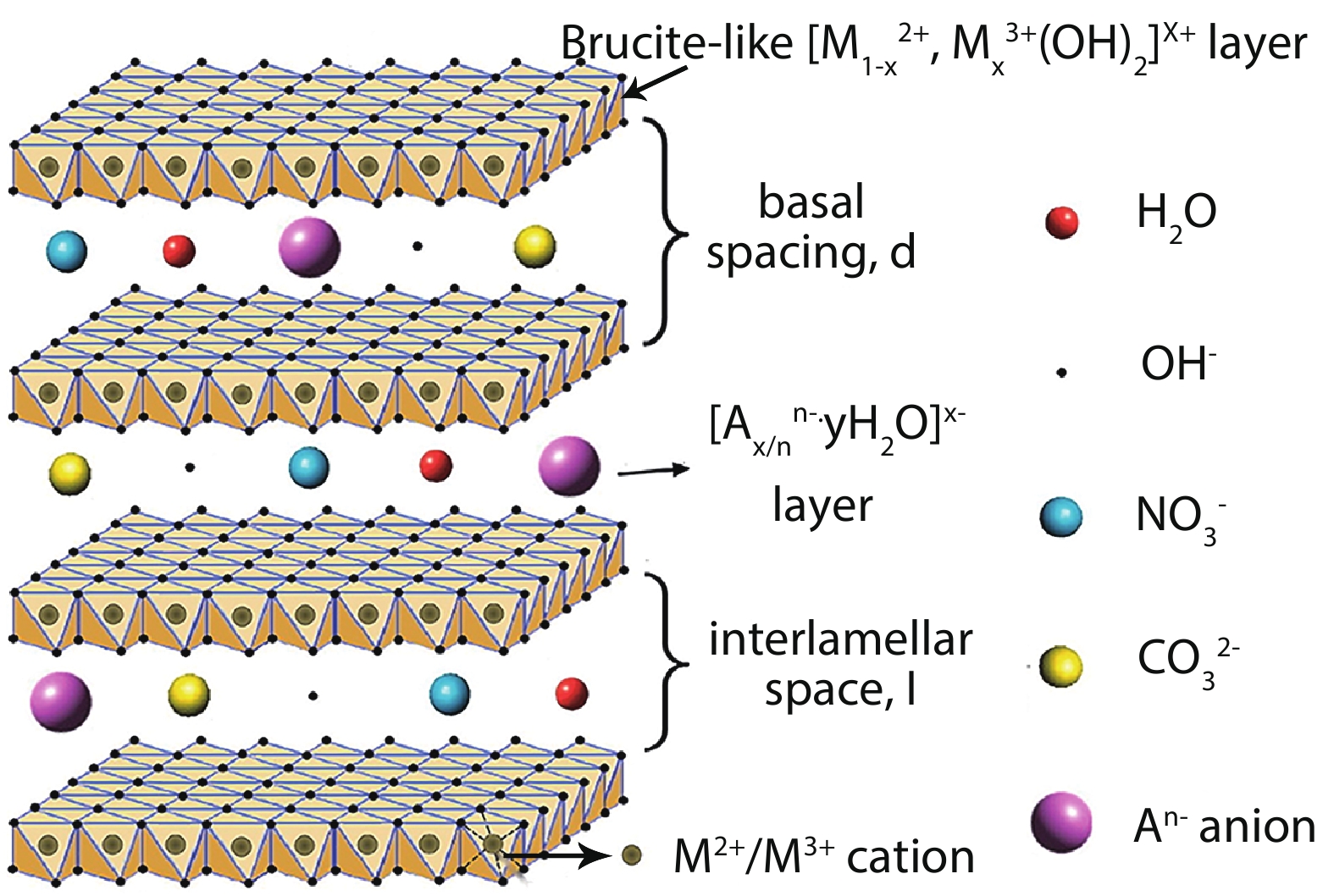
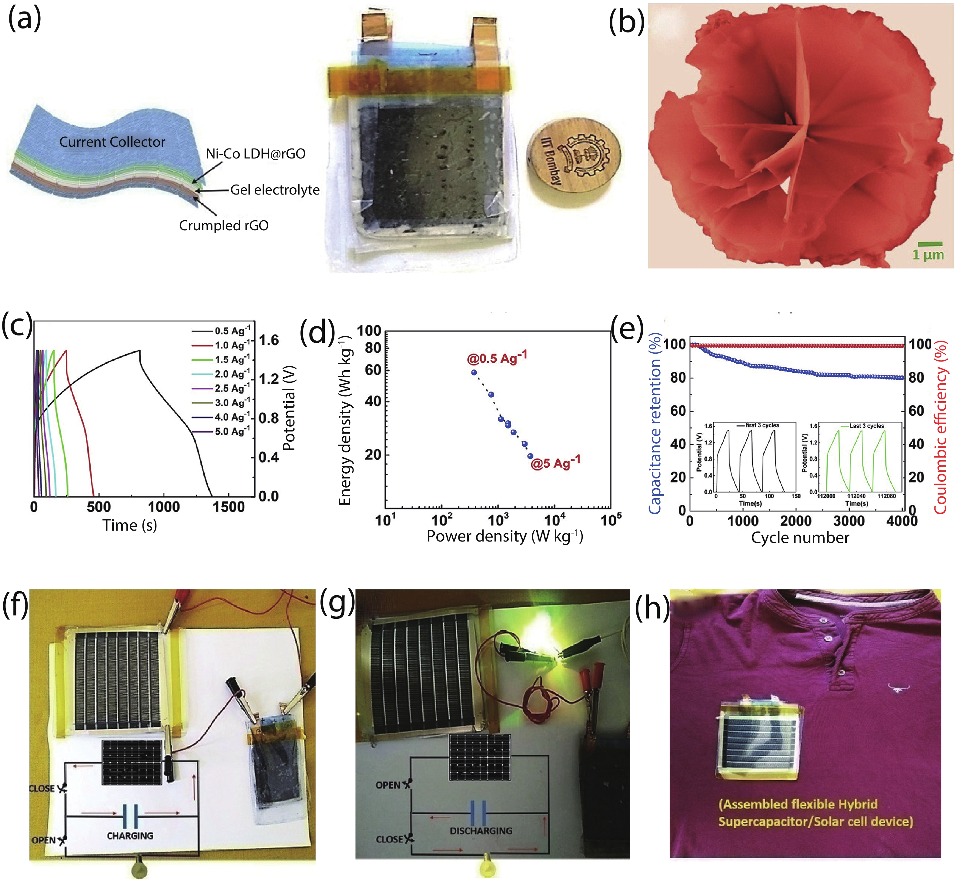
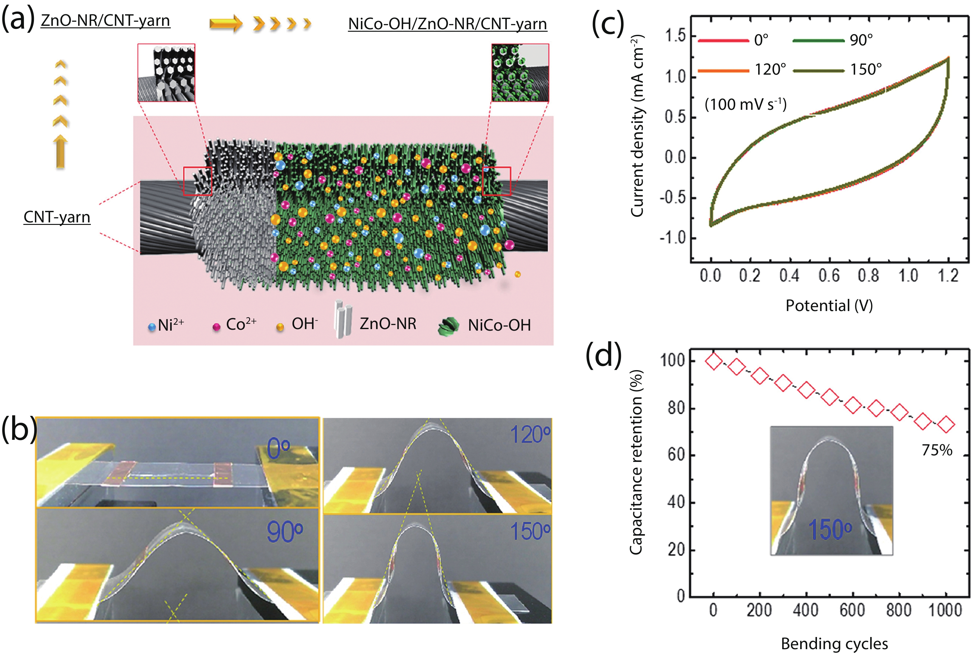
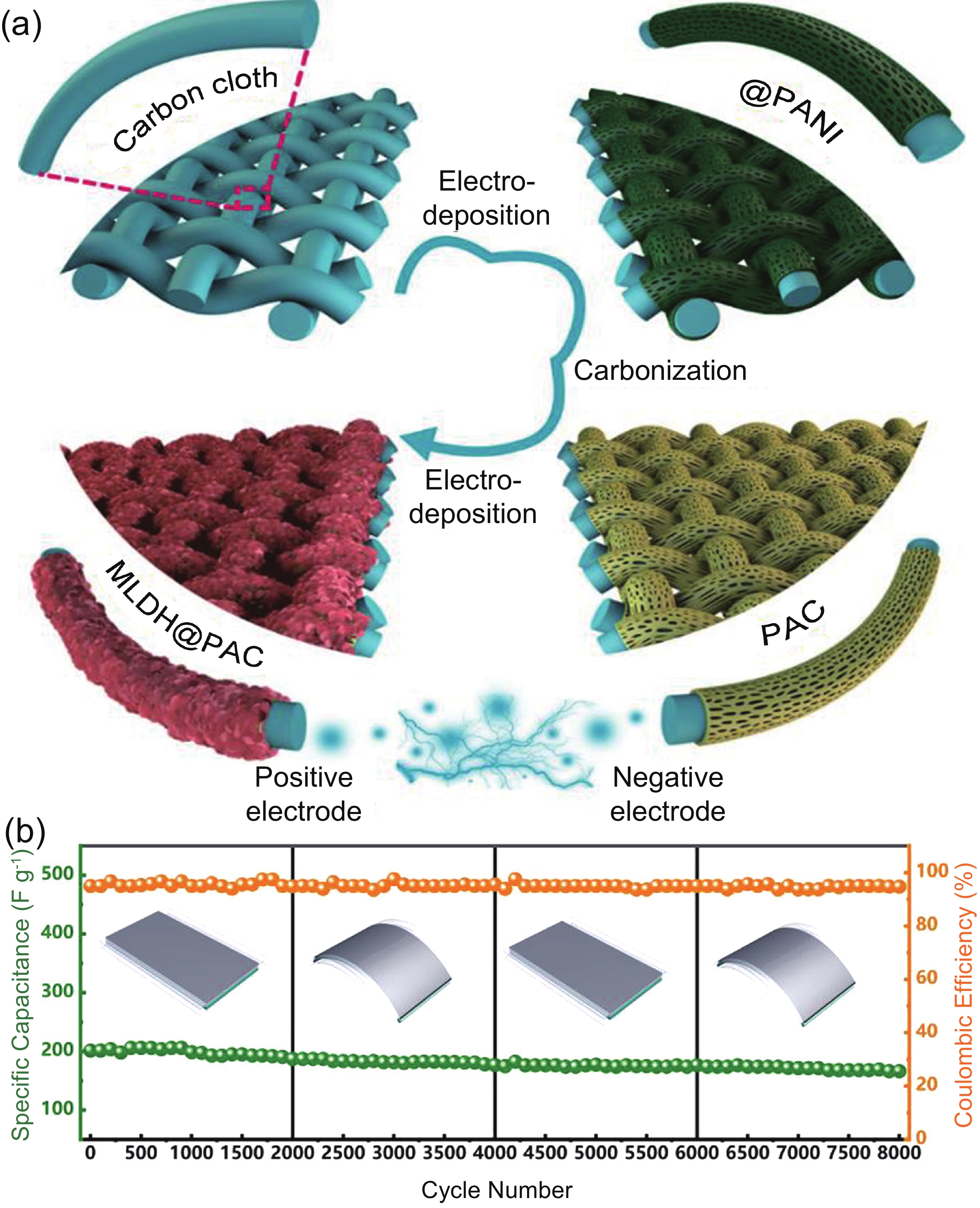
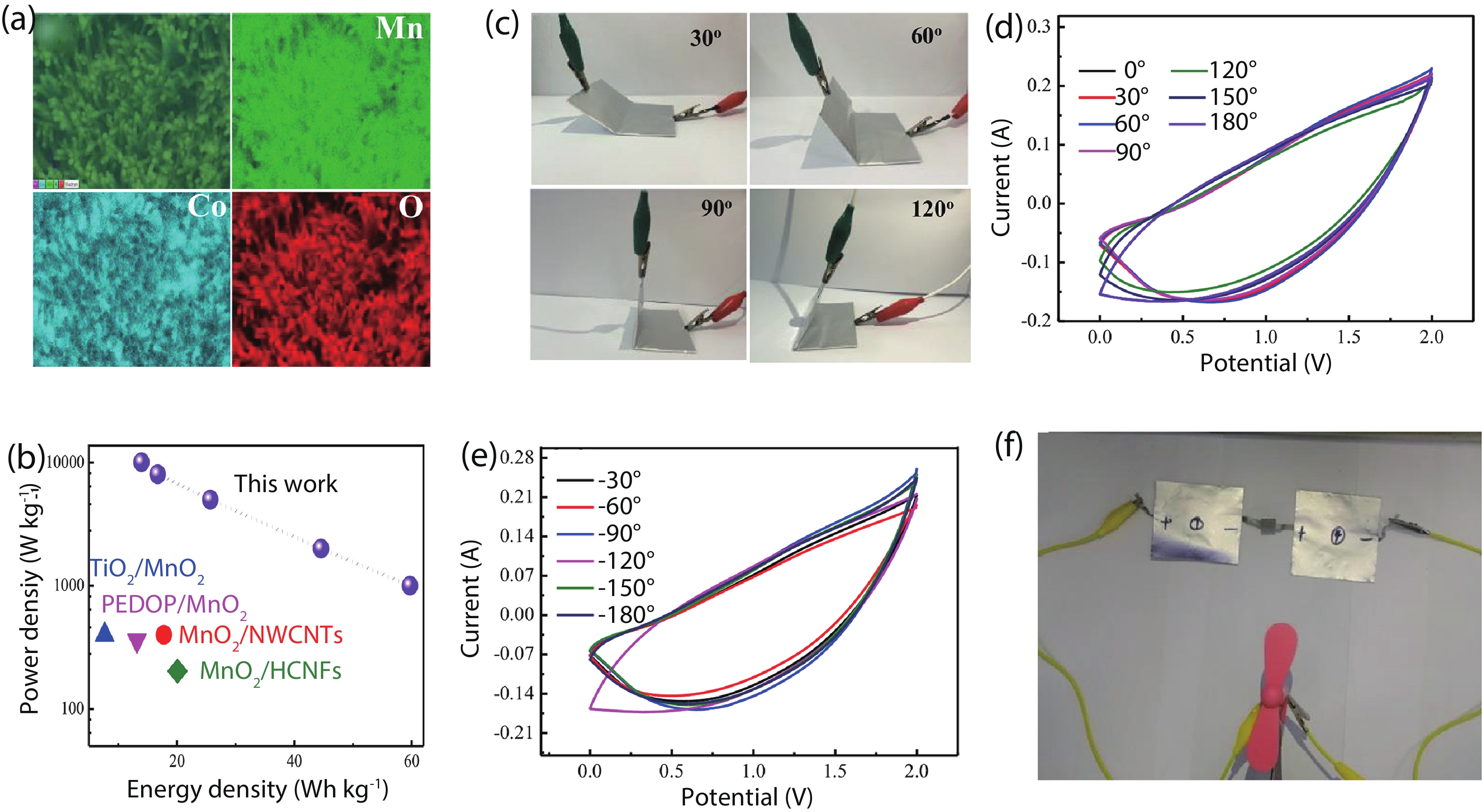
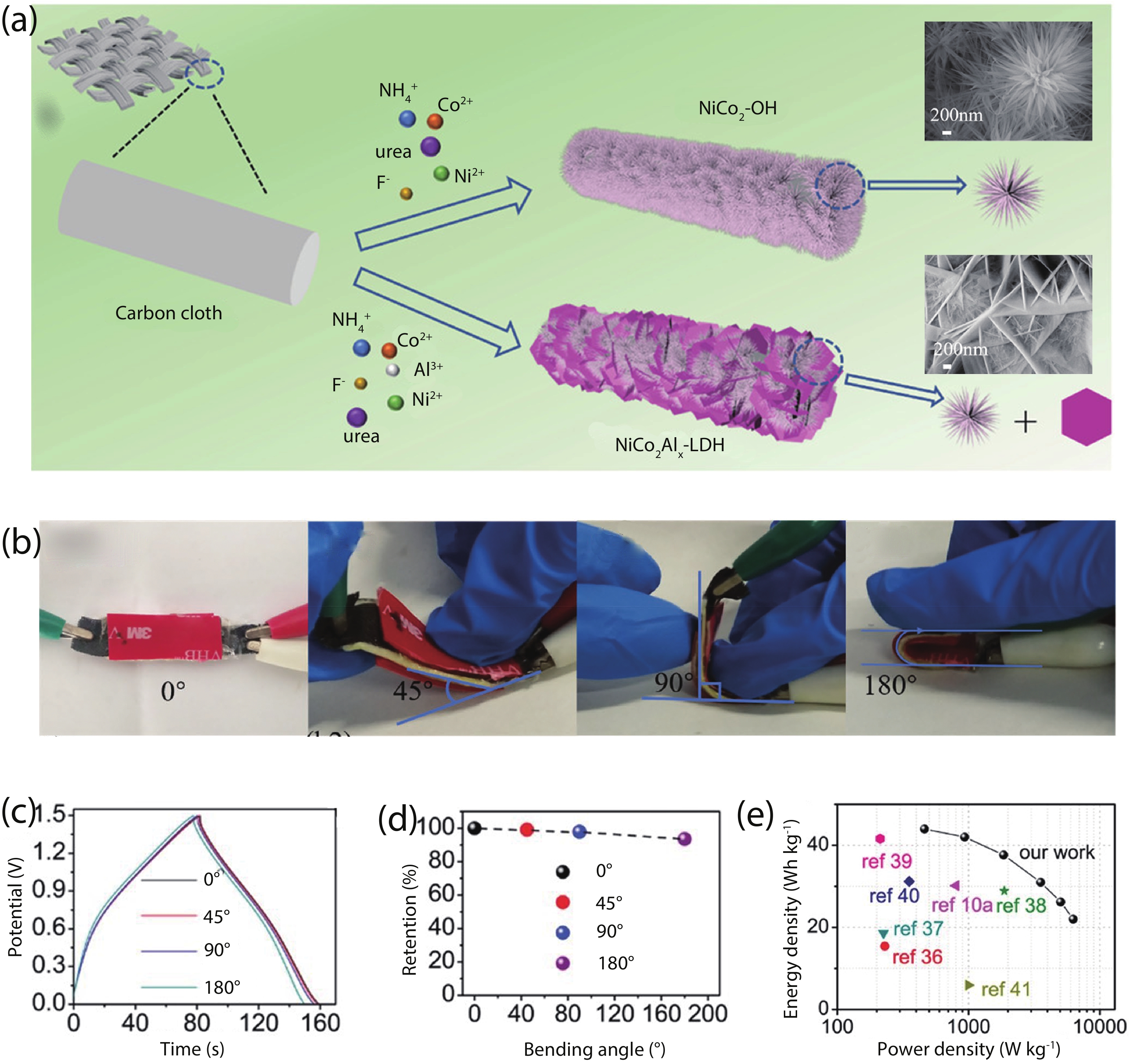
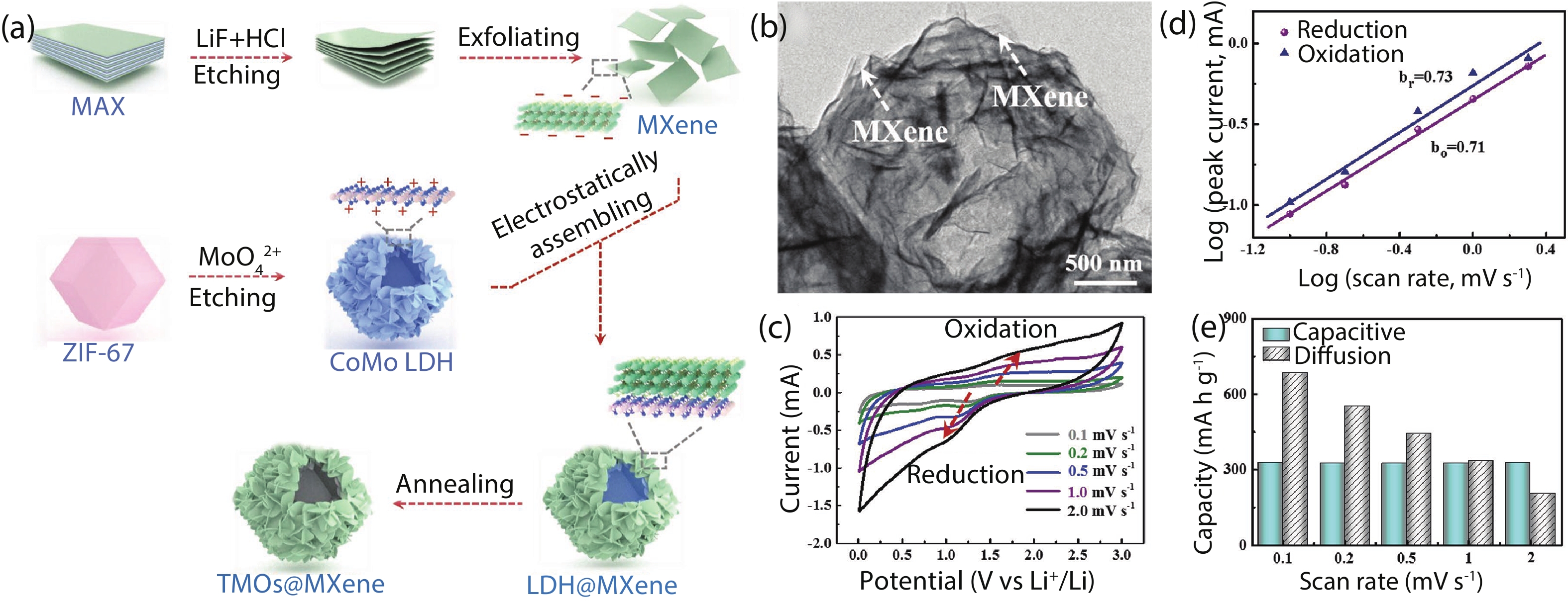
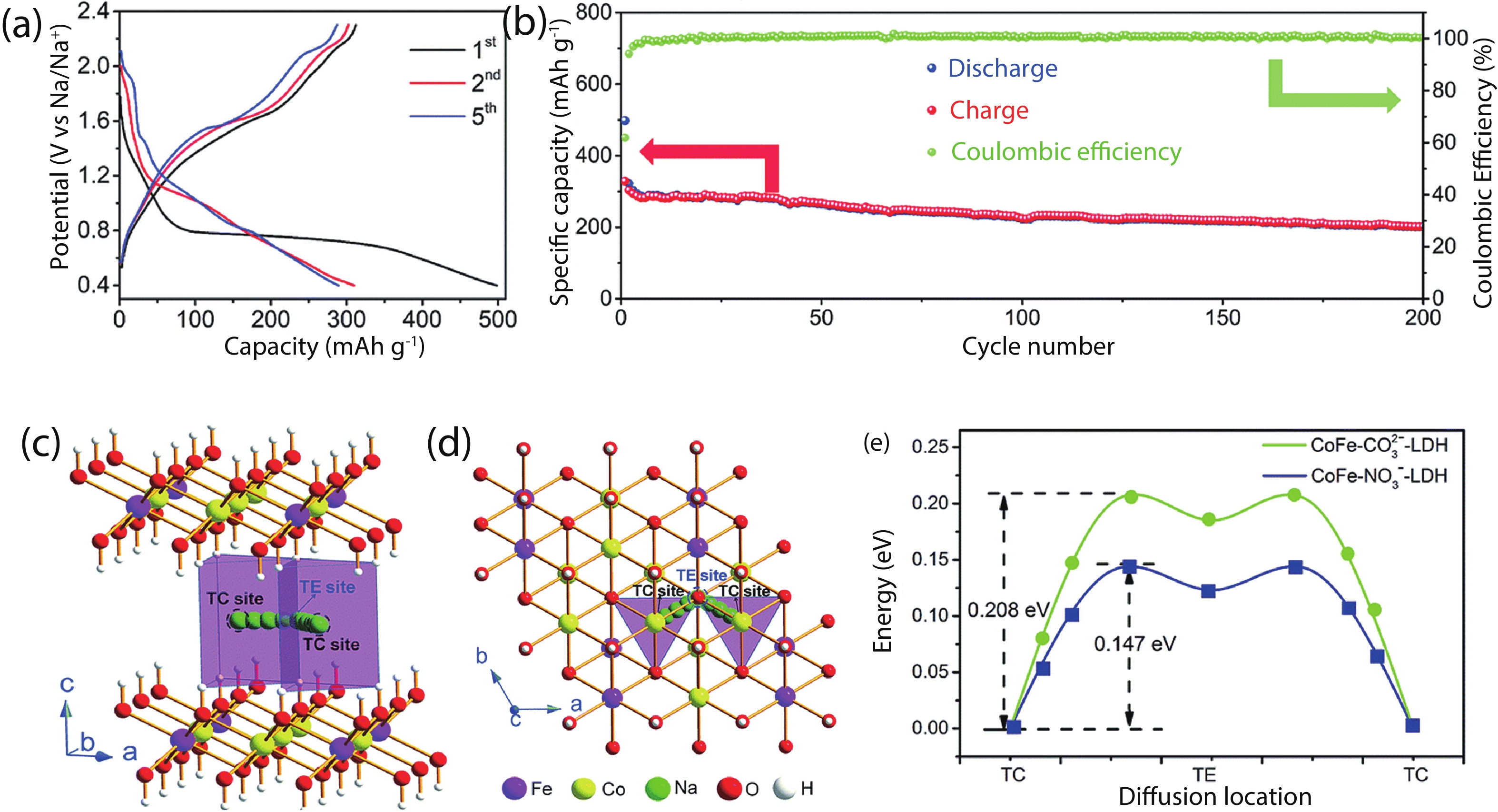
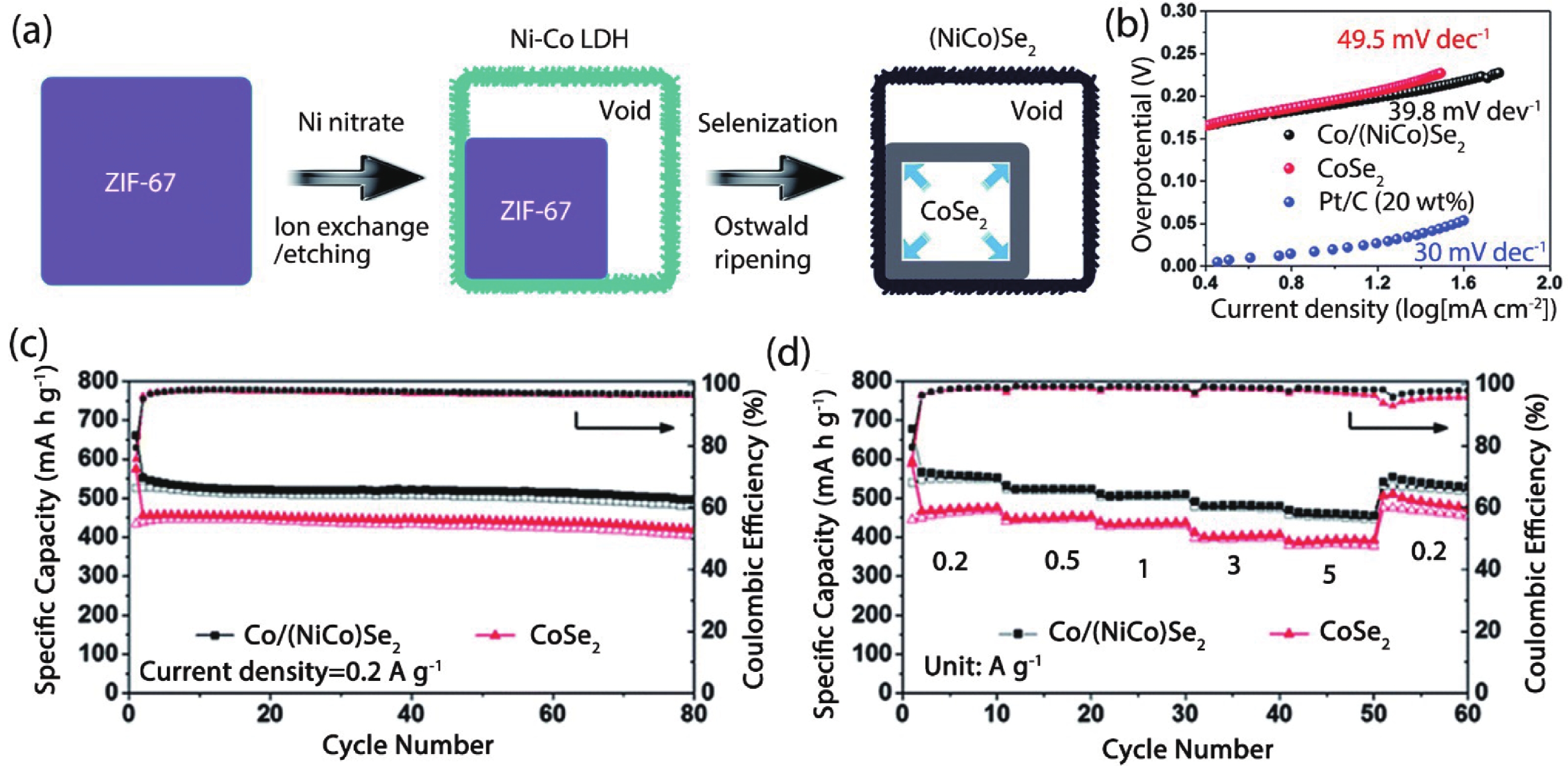
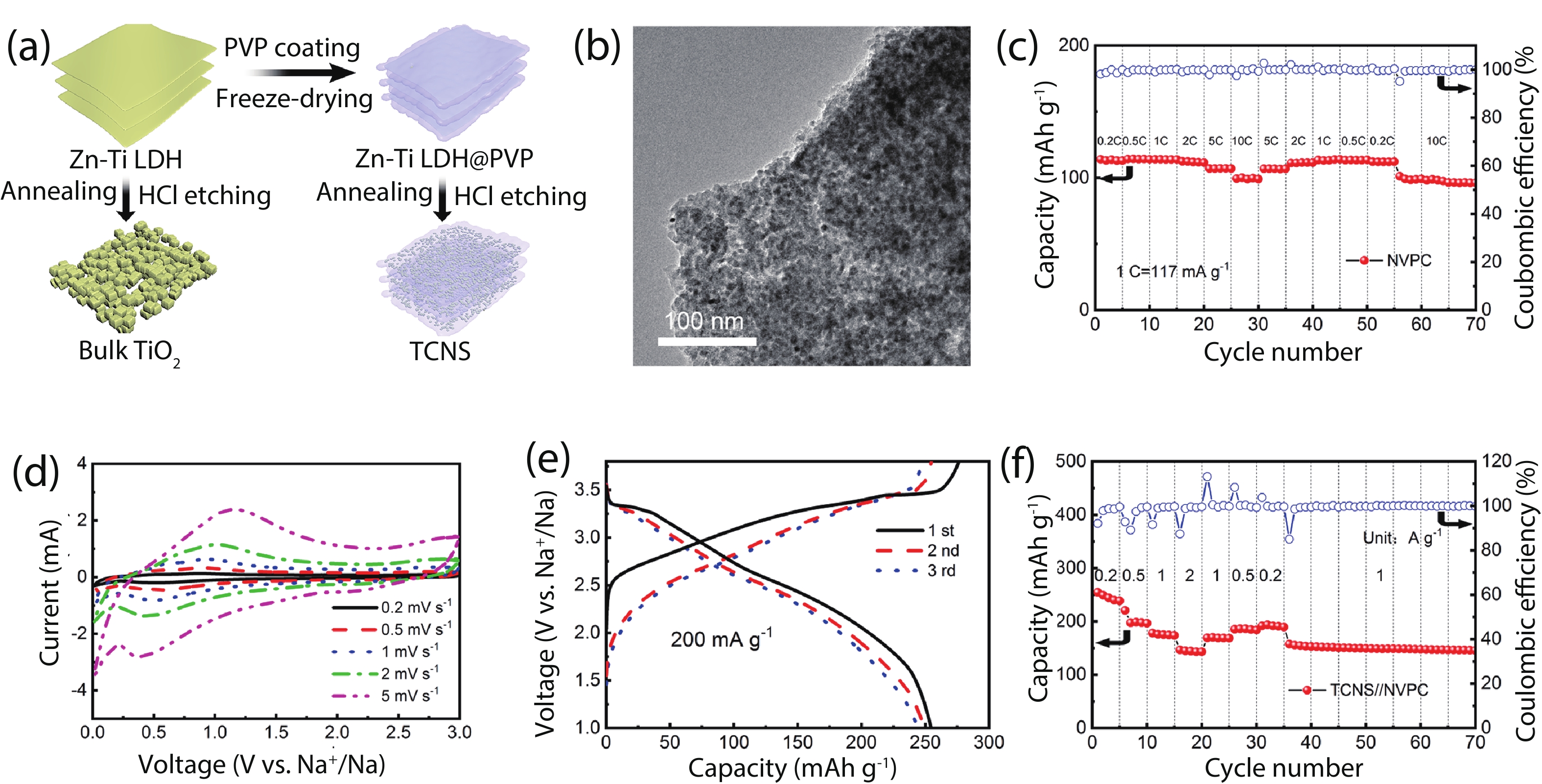
To prevent and mitigate environmental degradation, high-performance and cost-effective electrochemical flexible energy storage systems need to be urgently developed. This demand has led to an increase in research on electrode materials for high-capacity flexible supercapacitors and secondary batteries, which have greatly aided the development of contemporary digital communications and electric vehicles. The use of layered double hydroxides (LDHs) as electrode materials has shown productive results over the last decade, owing to their easy production, versatile composition, low cost, and excellent physicochemical features. This review highlights the distinctive 2D sheet-like structures and electrochemical characteristics of LDH materials, as well as current developments in their fabrication strategies for expanding the application scope of LDHs as electrode materials for flexible supercapacitors and alkali metal (Li, Na, K) ion batteries.


J. Semicond.
2023, 44(4): 041701 doi: 10.1088/1674-4926/44/4/041701
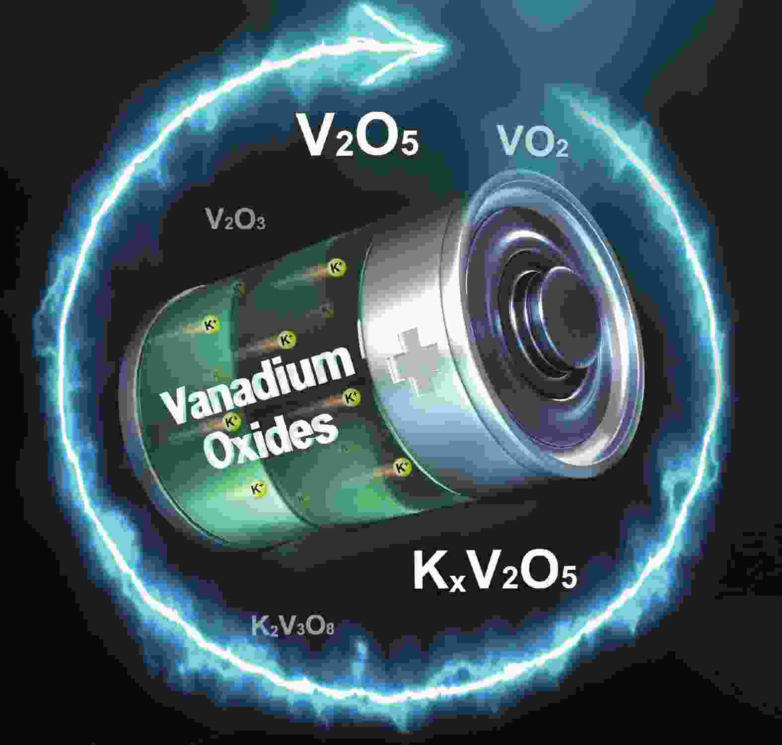
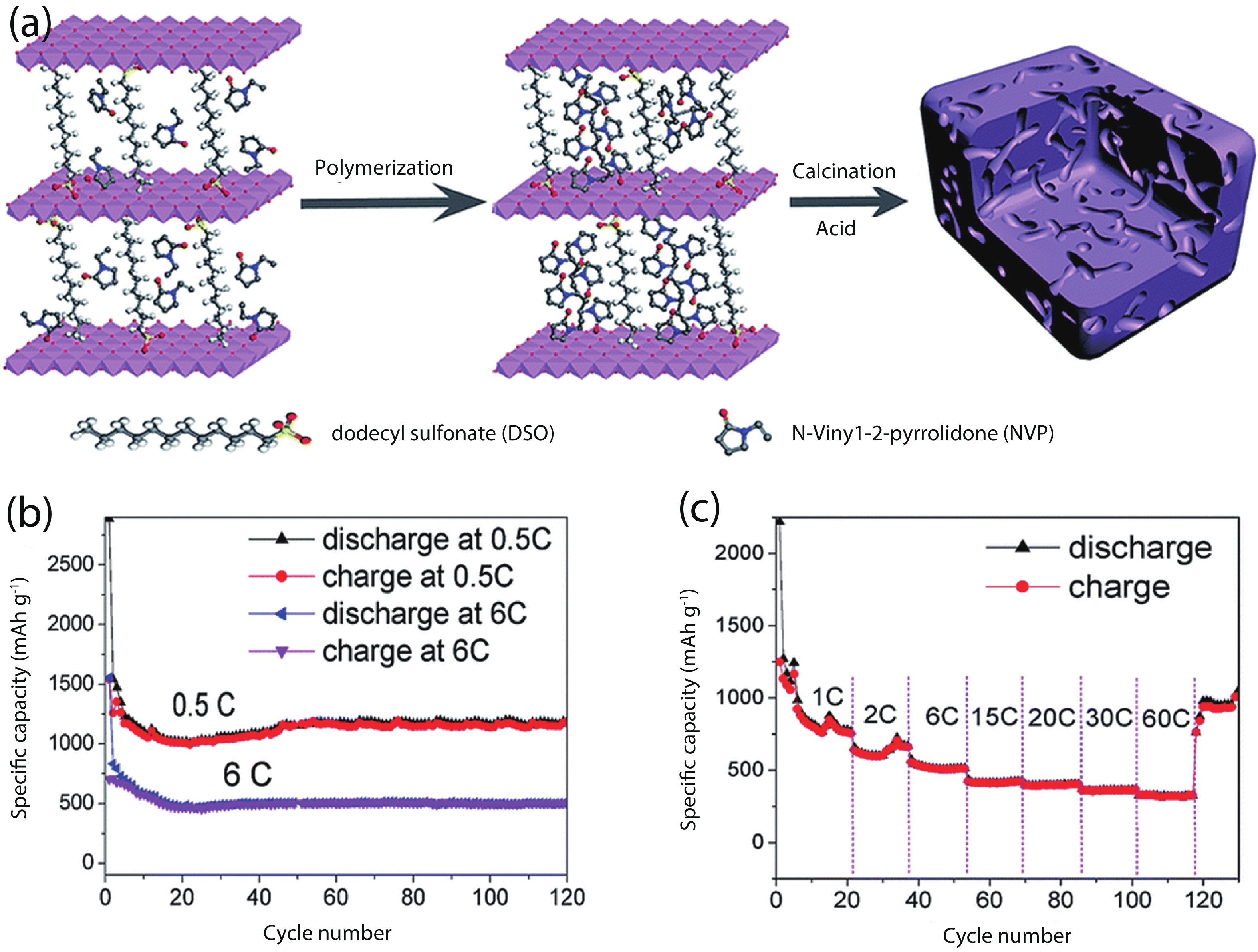
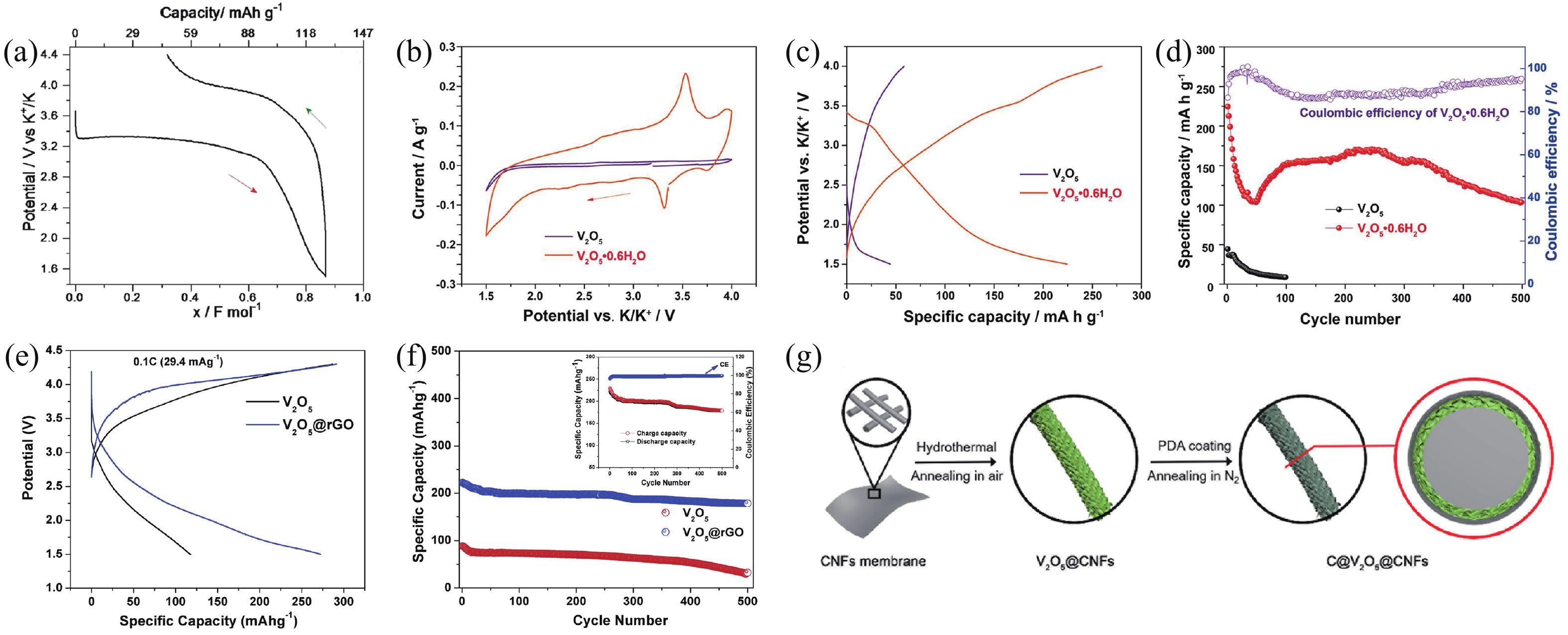
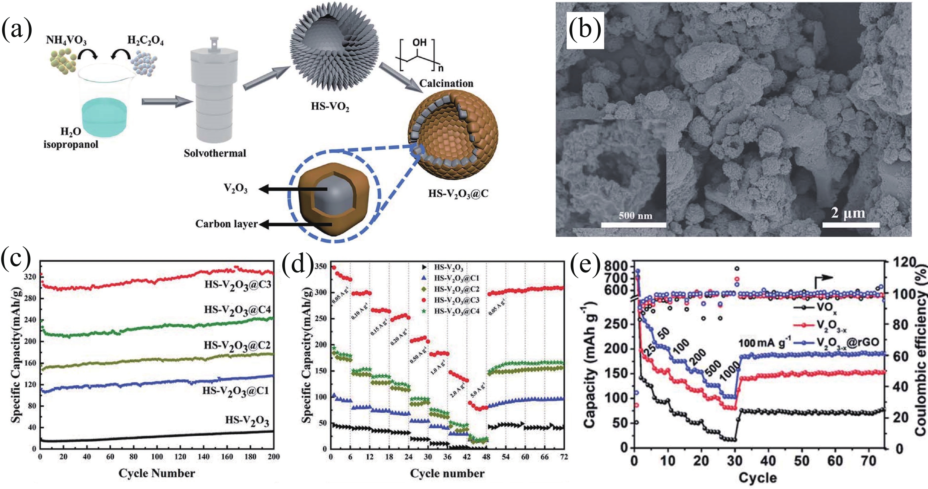
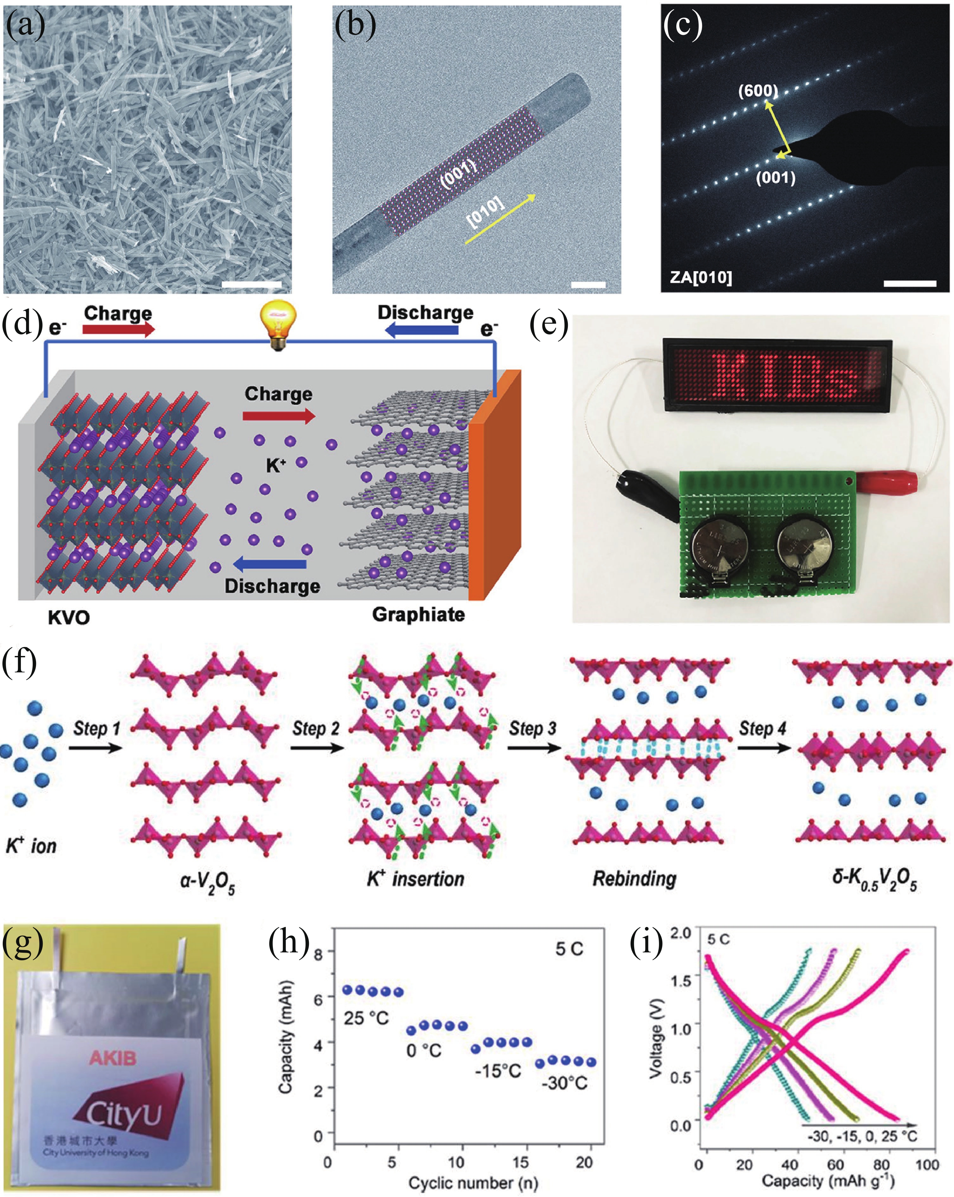
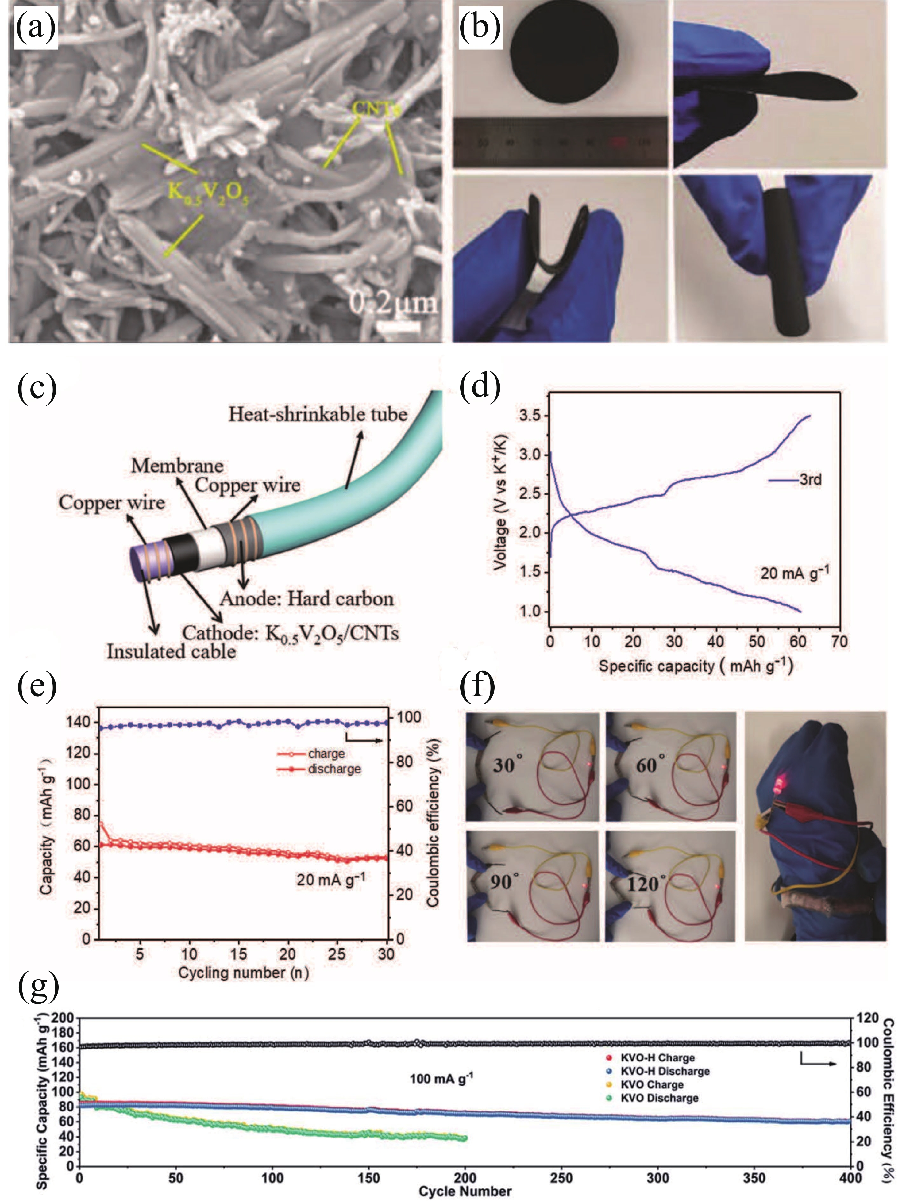
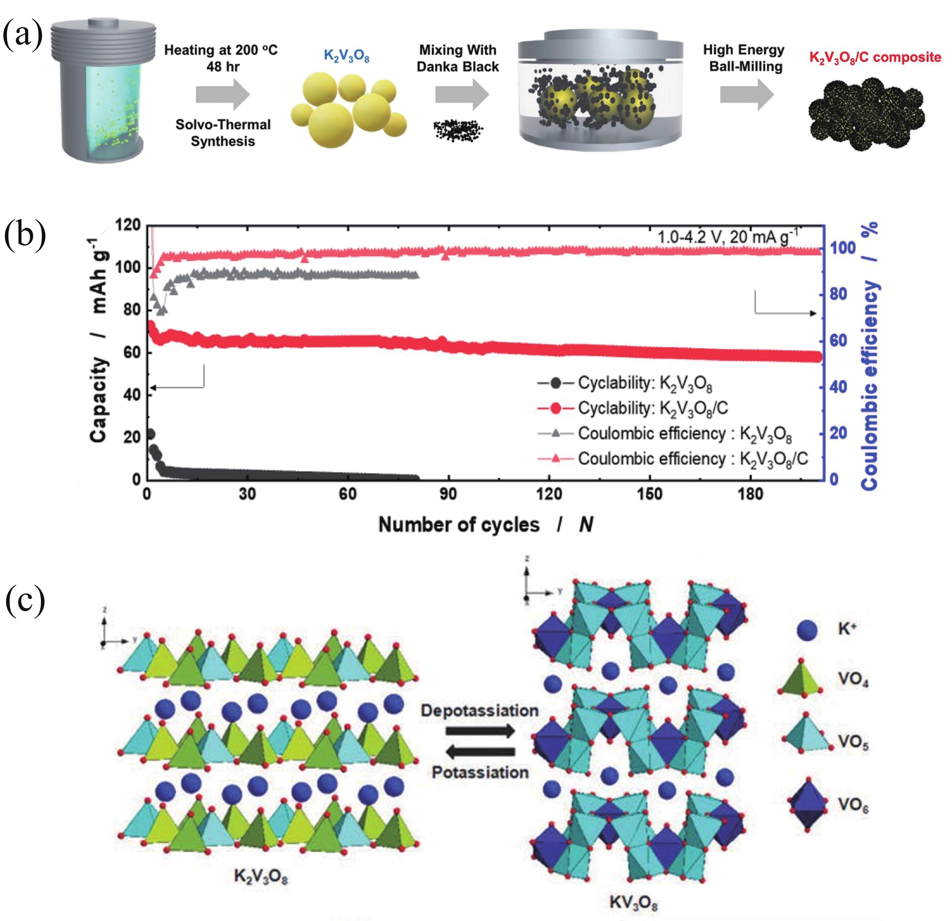
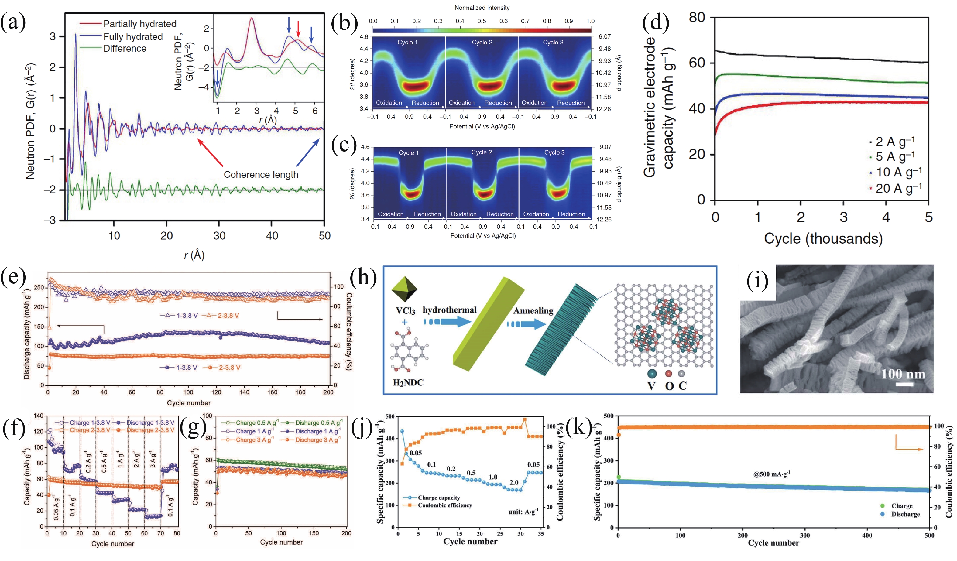
Potassium-ion batteries (PIBs) have been considered as promising candidates in the post-lithium-ion battery era. Till now, a large number of materials have been used as electrode materials for PIBs, among which vanadium oxides exhibit great potentiality. Vanadium oxides can provide multiple electron transfers during electrochemical reactions because vanadium possesses a variety of oxidation states. Meanwhile, their relatively low cost and superior material, structural, and physicochemical properties endow them with strong competitiveness. Although some inspiring research results have been achieved, many issues and challenges remain to be further addressed. Herein, we systematically summarize the research progress of vanadium oxides for PIBs. Then, feasible improvement strategies for the material properties and electrochemical performance are introduced. Finally, the existing challenges and perspectives are discussed with a view to promoting the development of vanadium oxides and accelerating their practical applications.


J. Semicond.
2023, 44(4): 041901 doi: 10.1088/1674-4926/44/4/041901
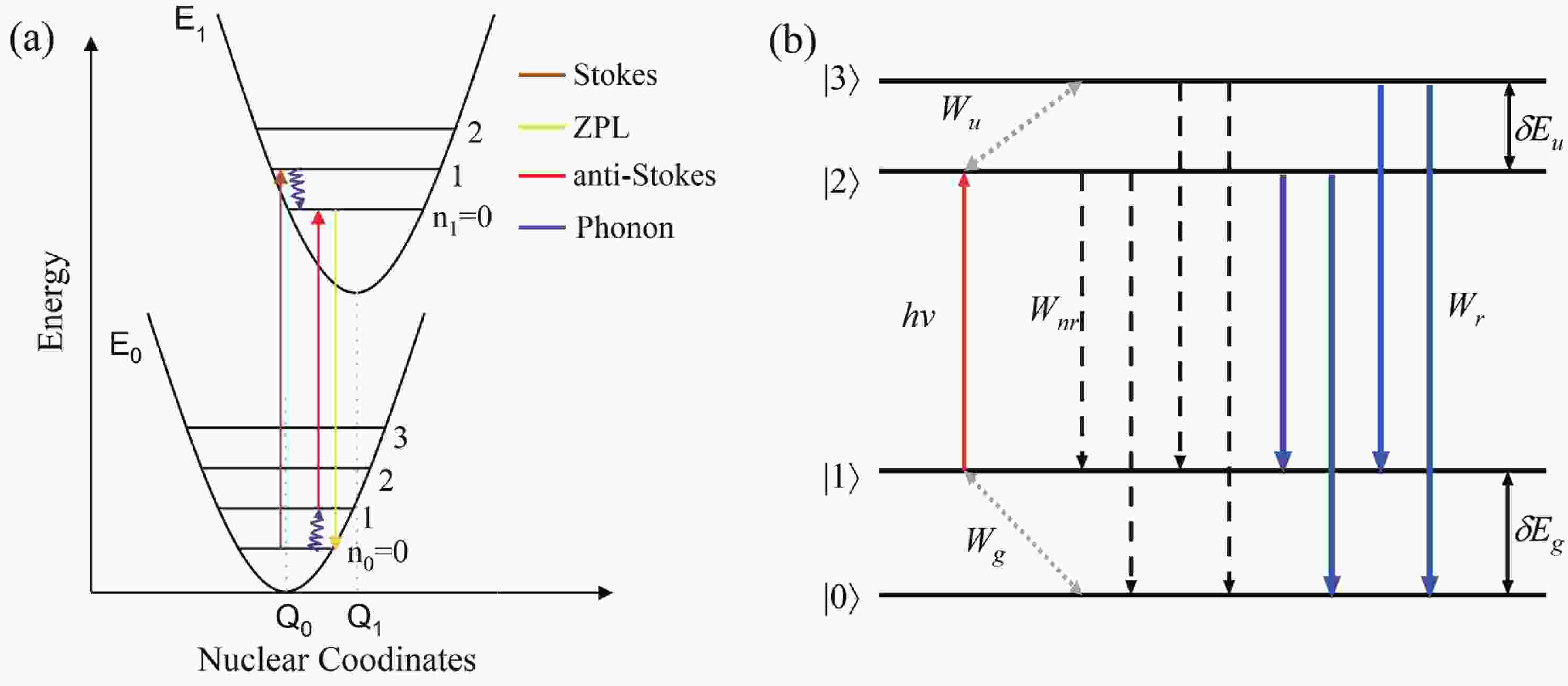
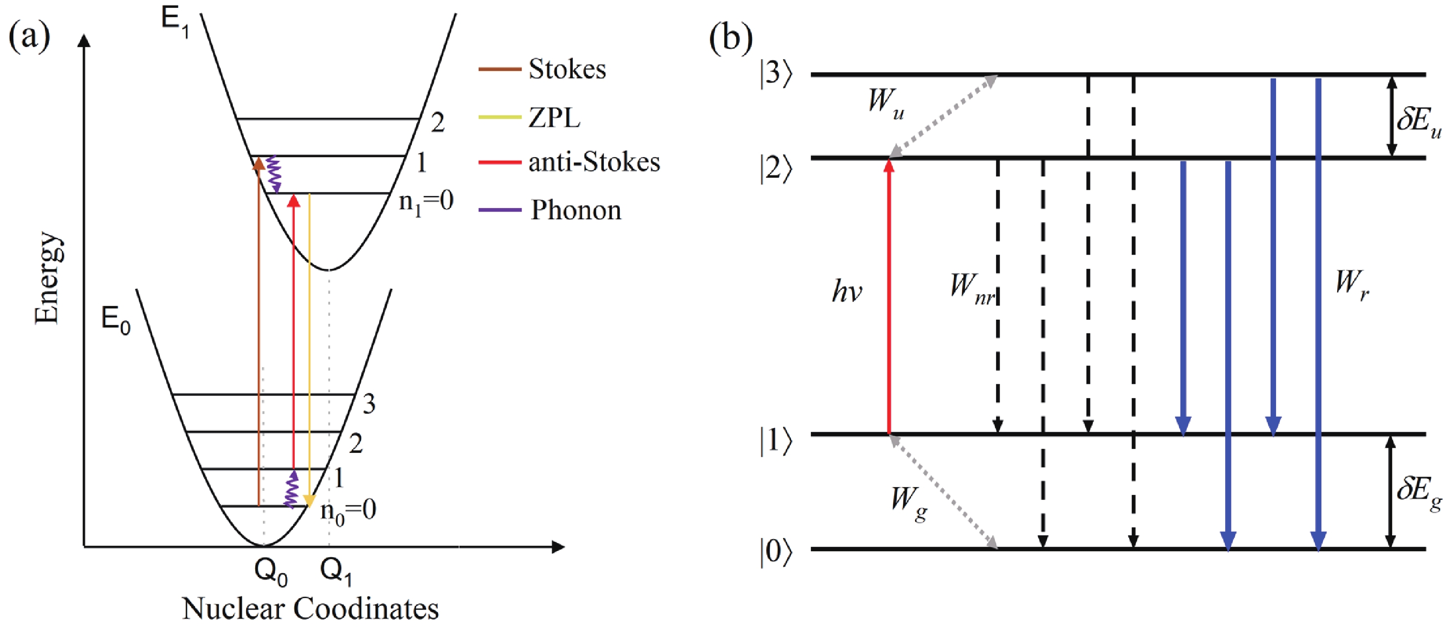
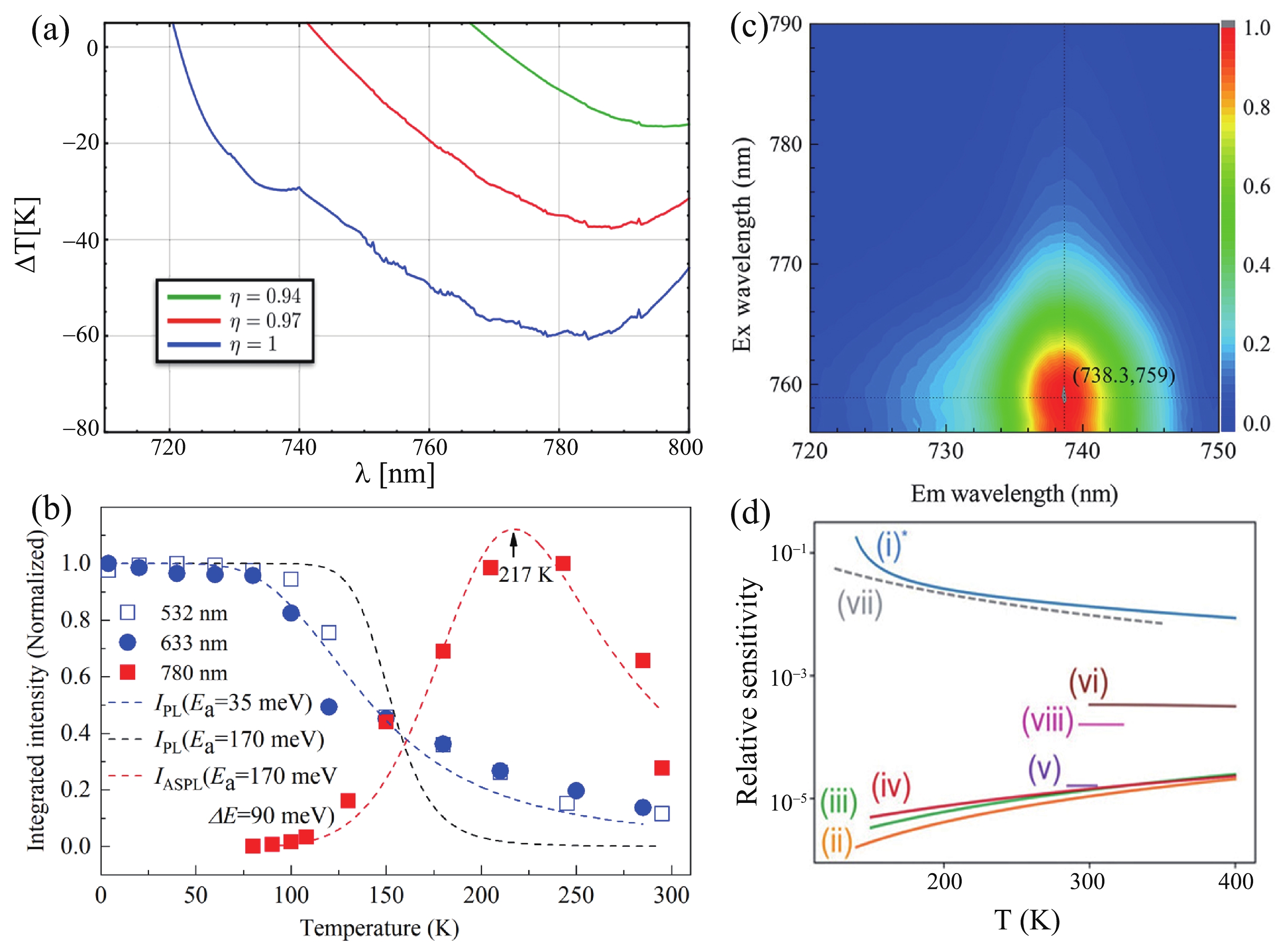
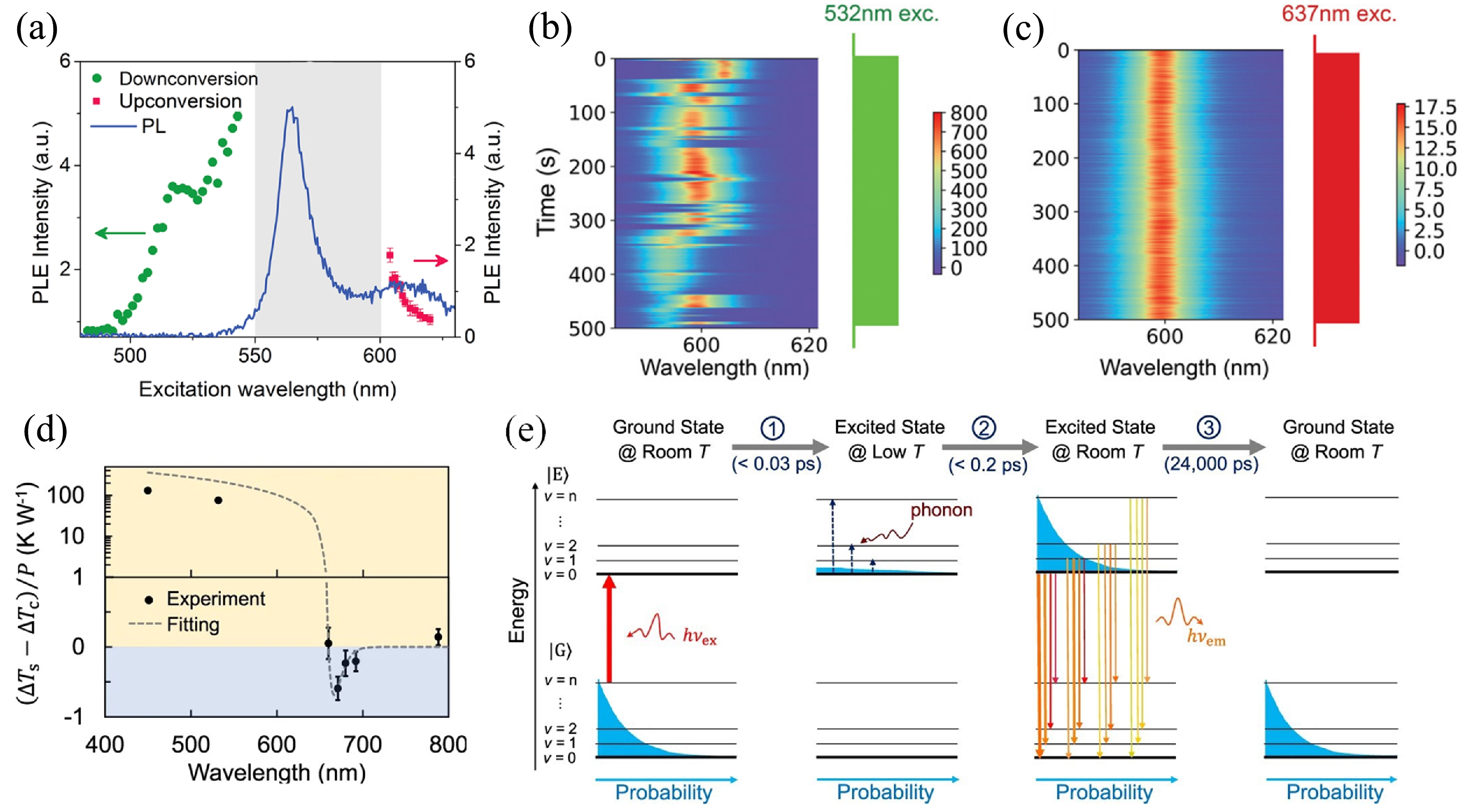
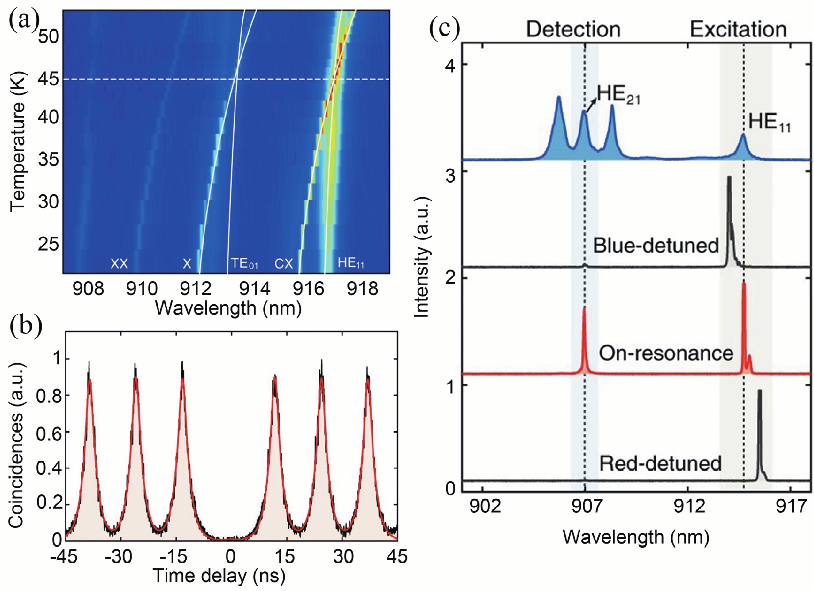
Quantum emitters are widely used in quantum networks, quantum information processing, and quantum sensing due to their excellent optical properties. Compared with Stokes excitation, quantum emitters under anti-Stokes excitation exhibit better performance. In addition to laser cooling and nanoscale thermometry, anti-Stokes excitation can improve the coherence of single-photon sources for advanced quantum technologies. In this review, we follow the recent advances in phonon-assisted upconversion photoluminescence of quantum emitters and discuss the upconversion mechanisms, applications, and prospects for quantum emitters with anti-Stokes excitation.

J. Semicond.
2023, 44(4): 042101 doi: 10.1088/1674-4926/44/4/042101
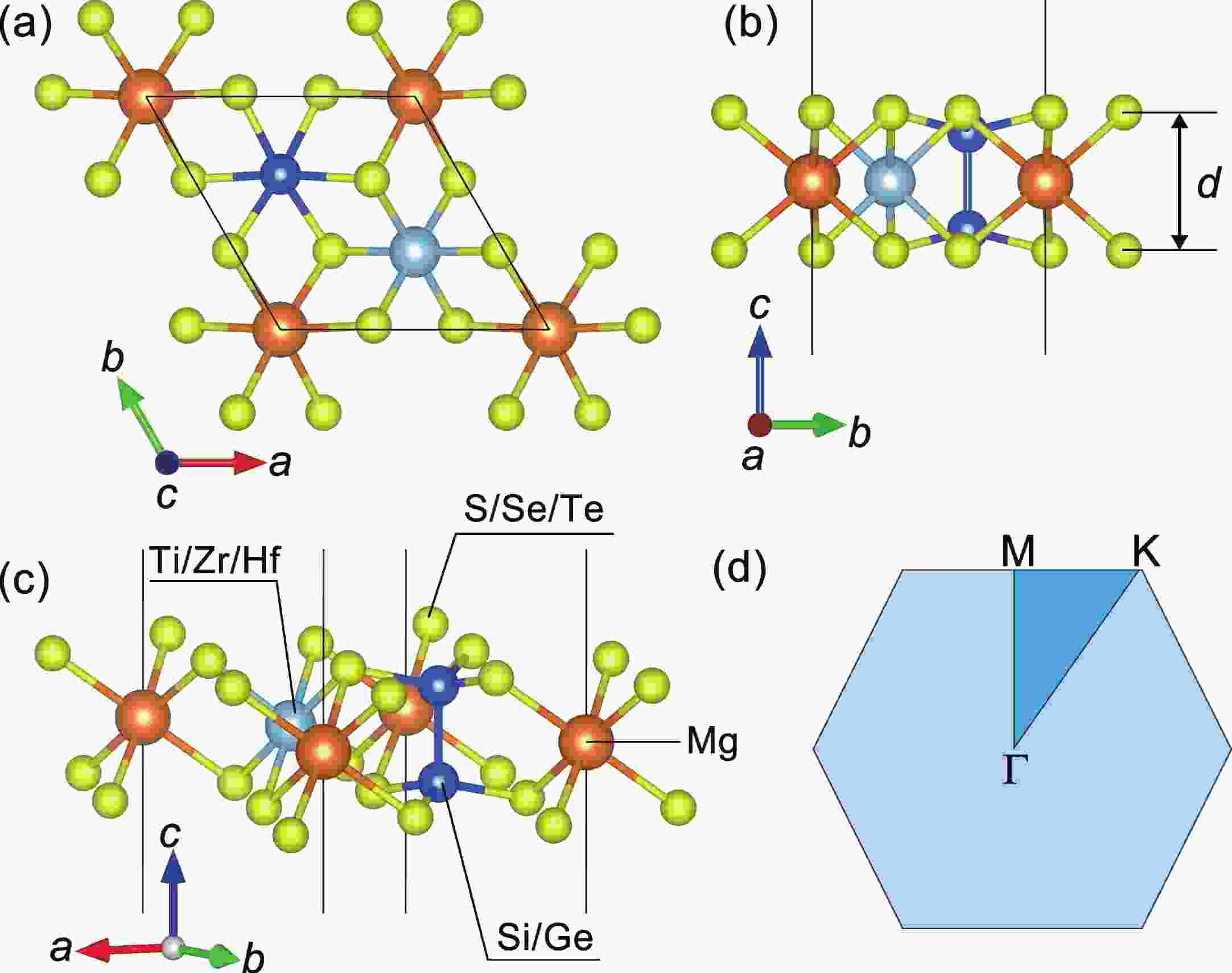
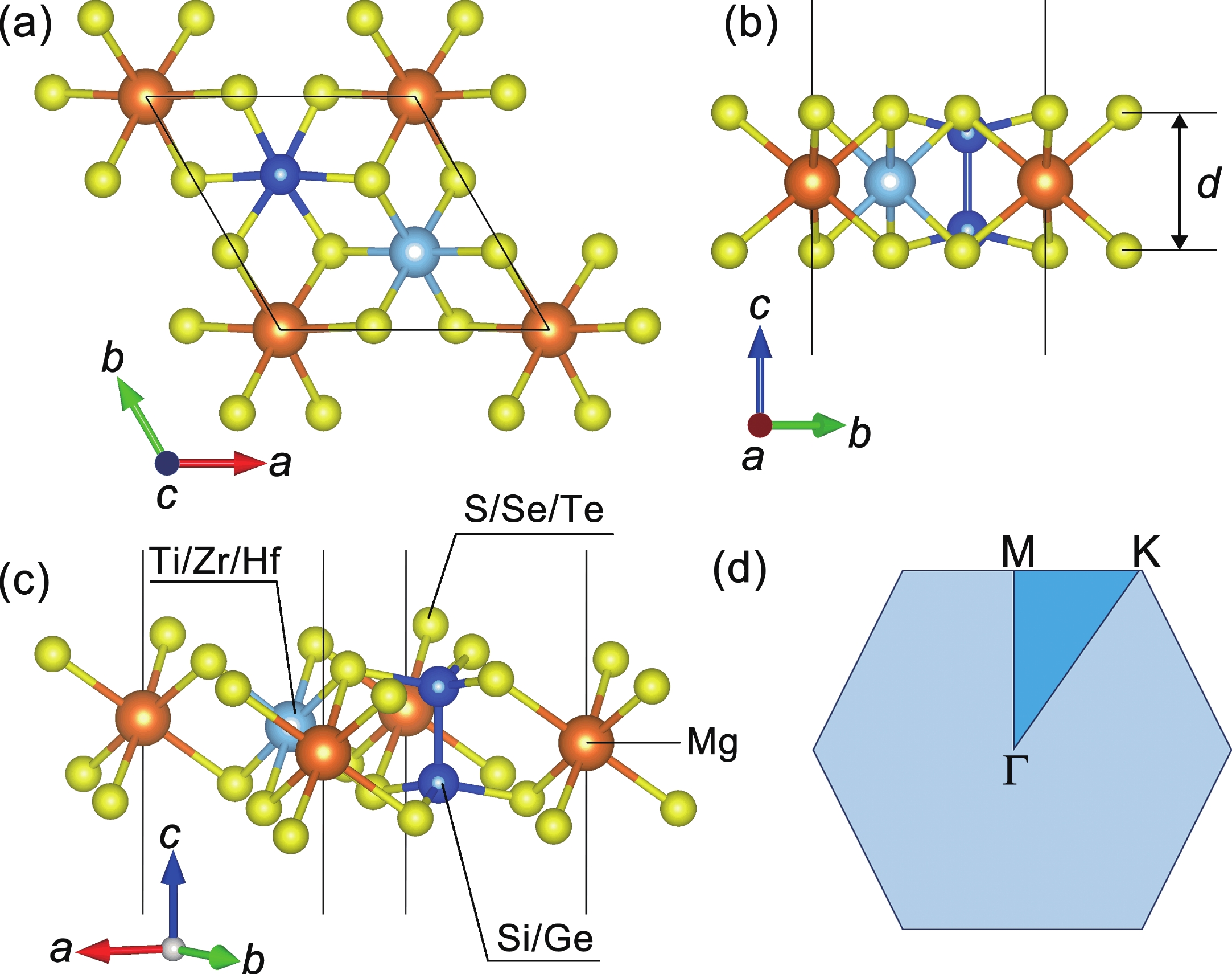
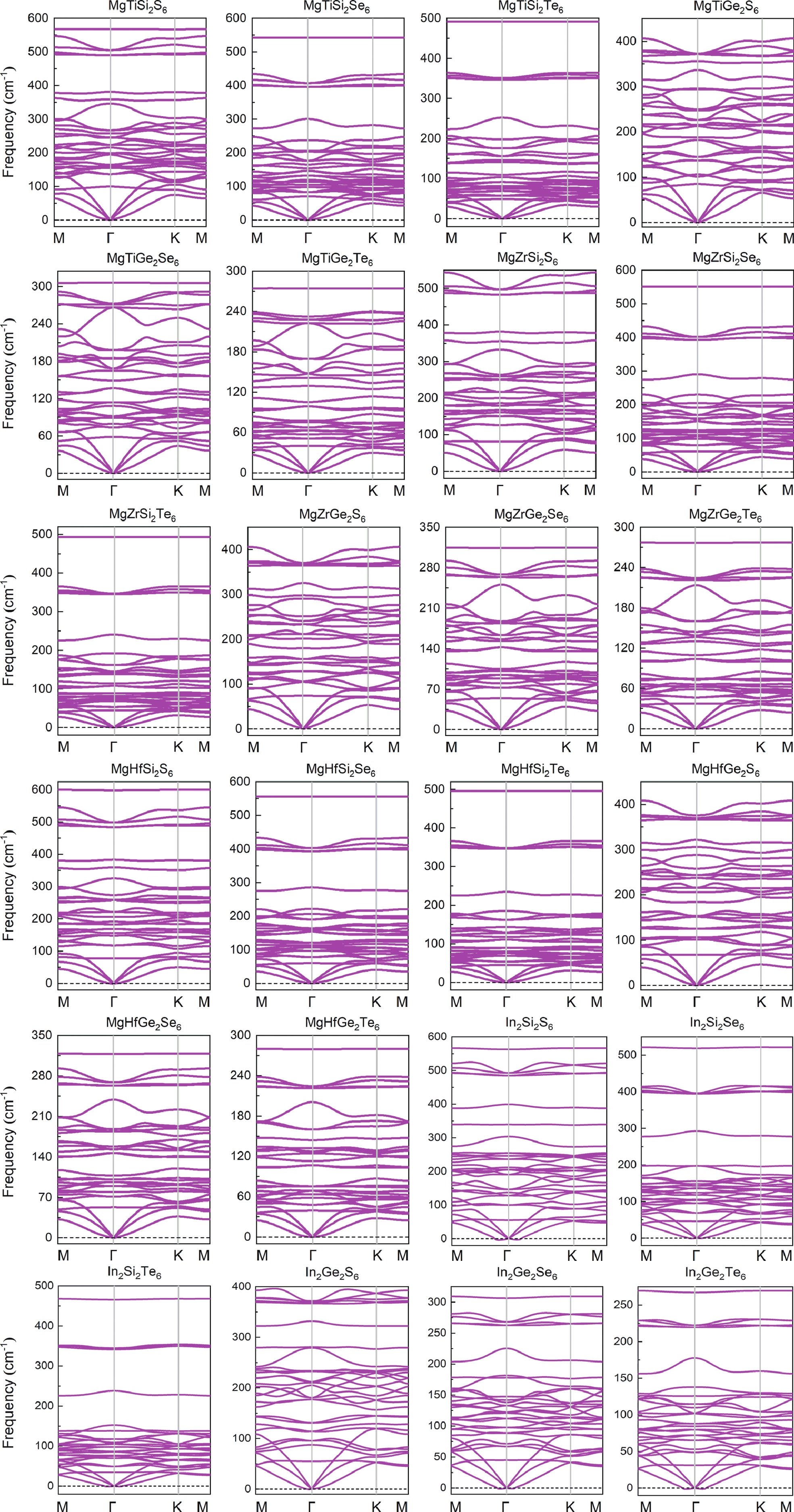
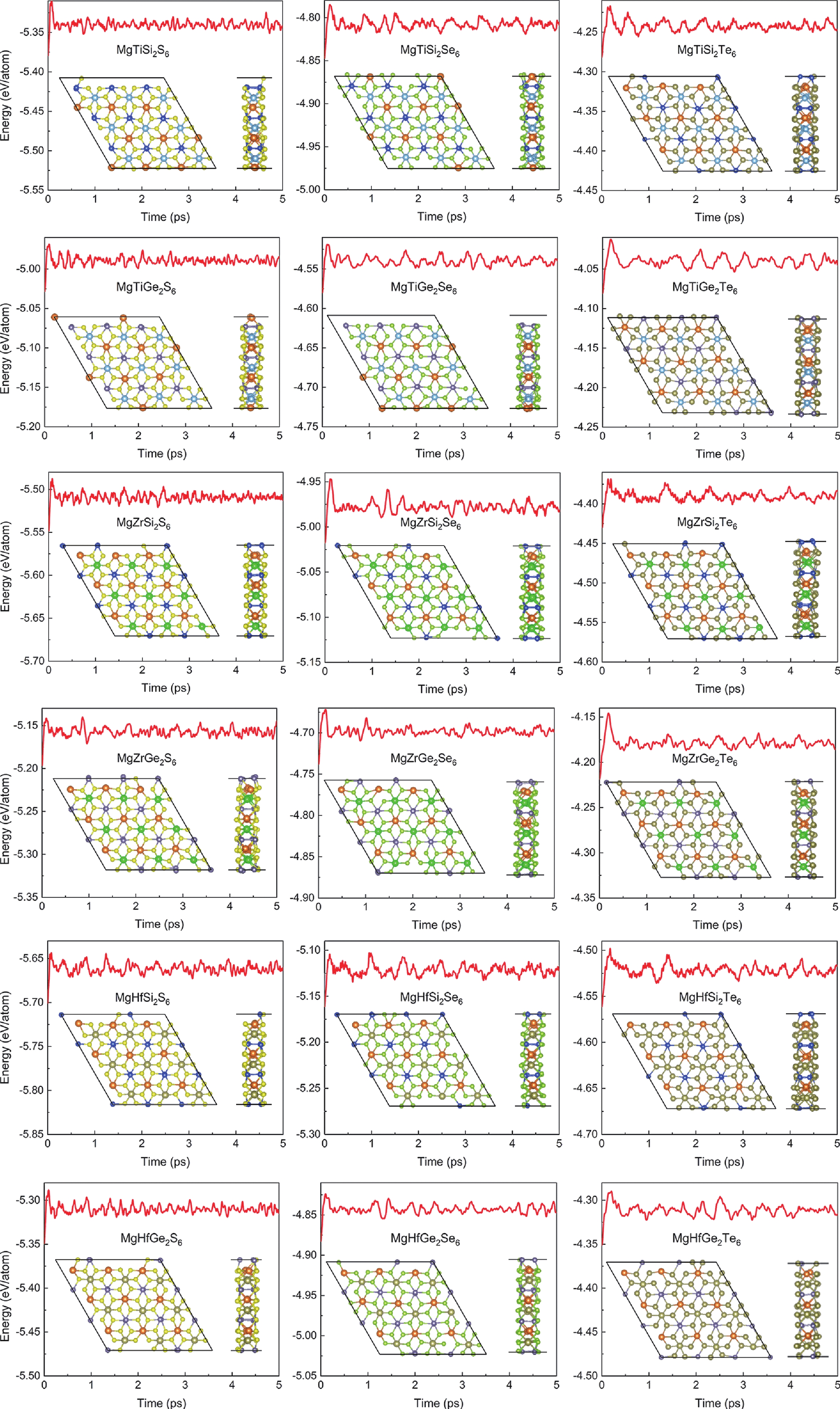
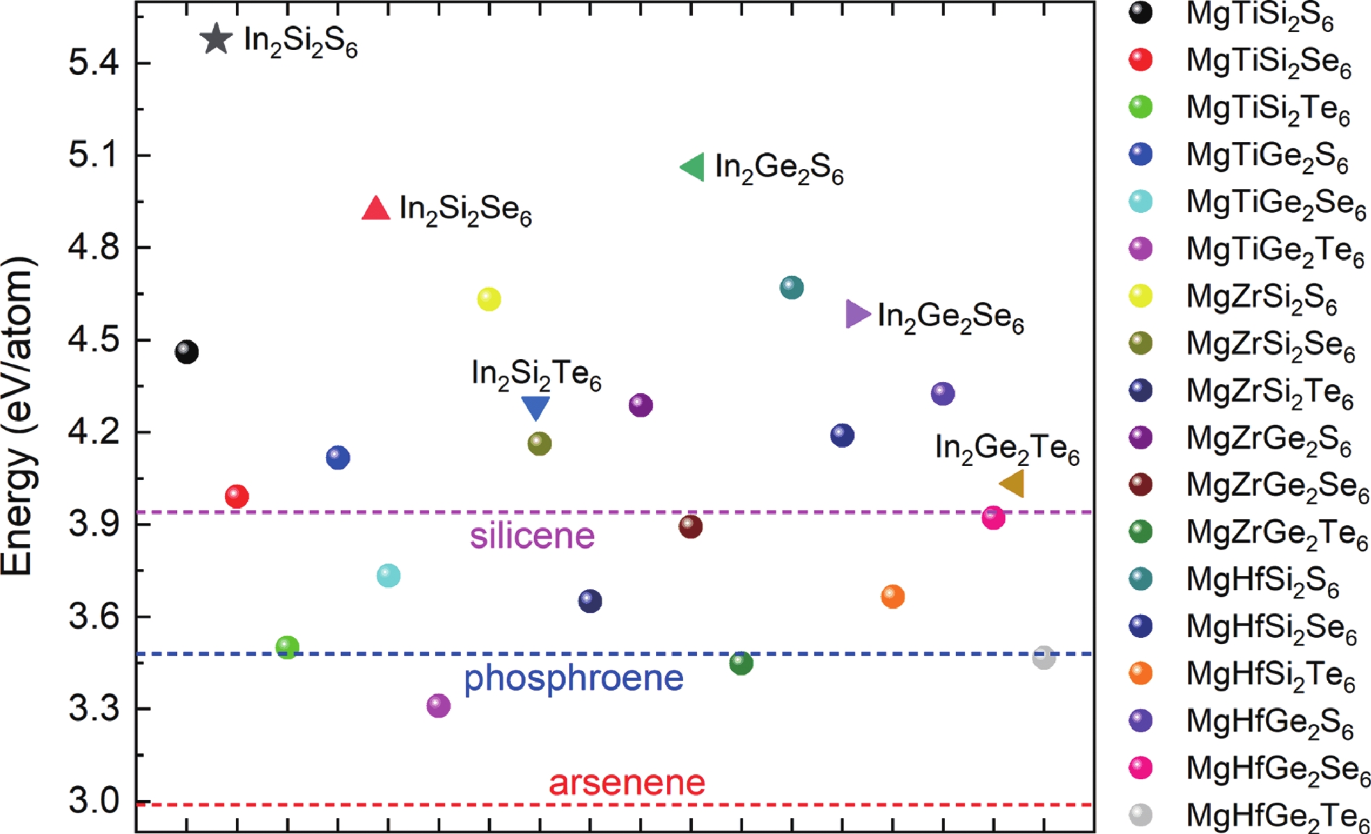
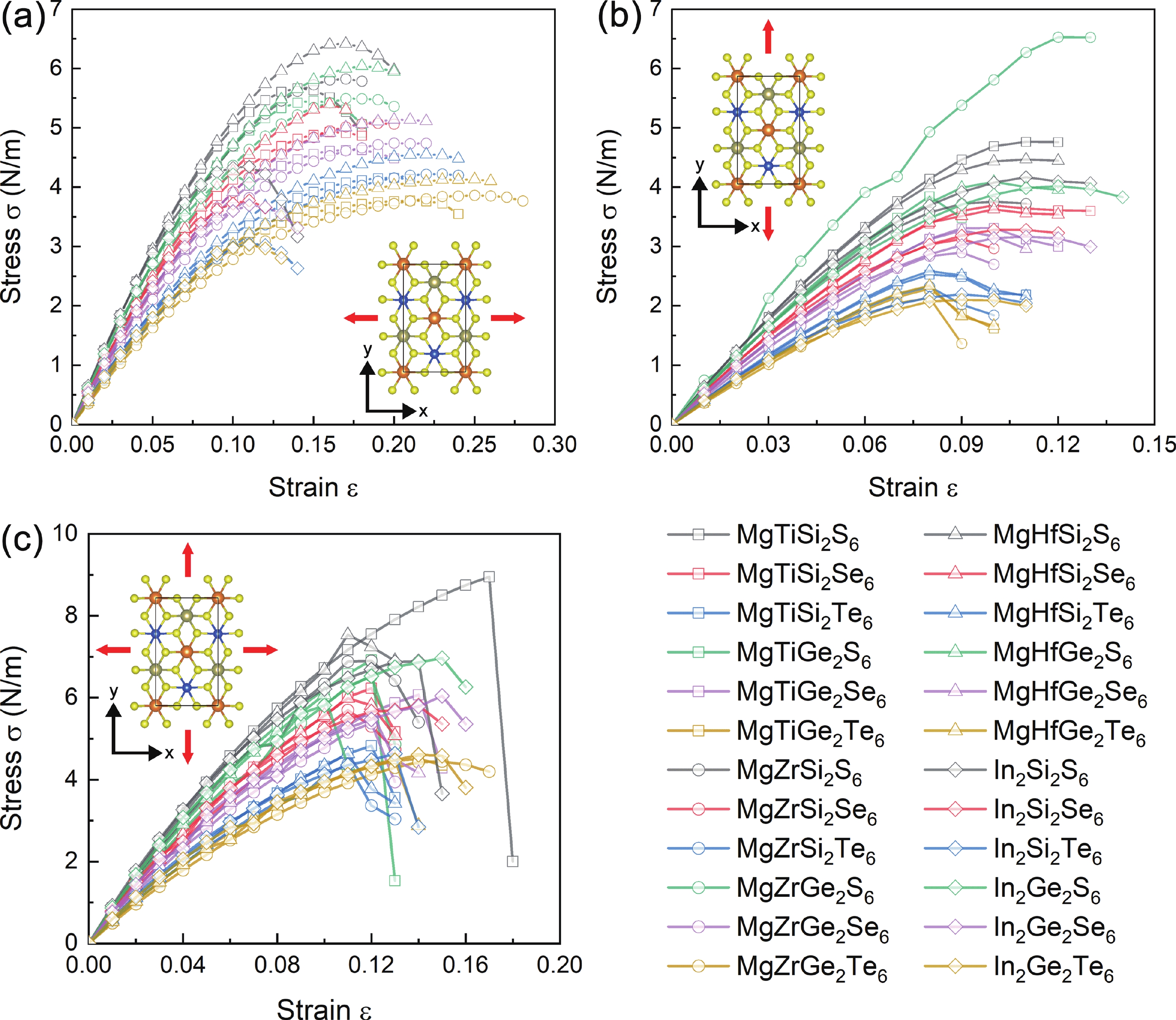
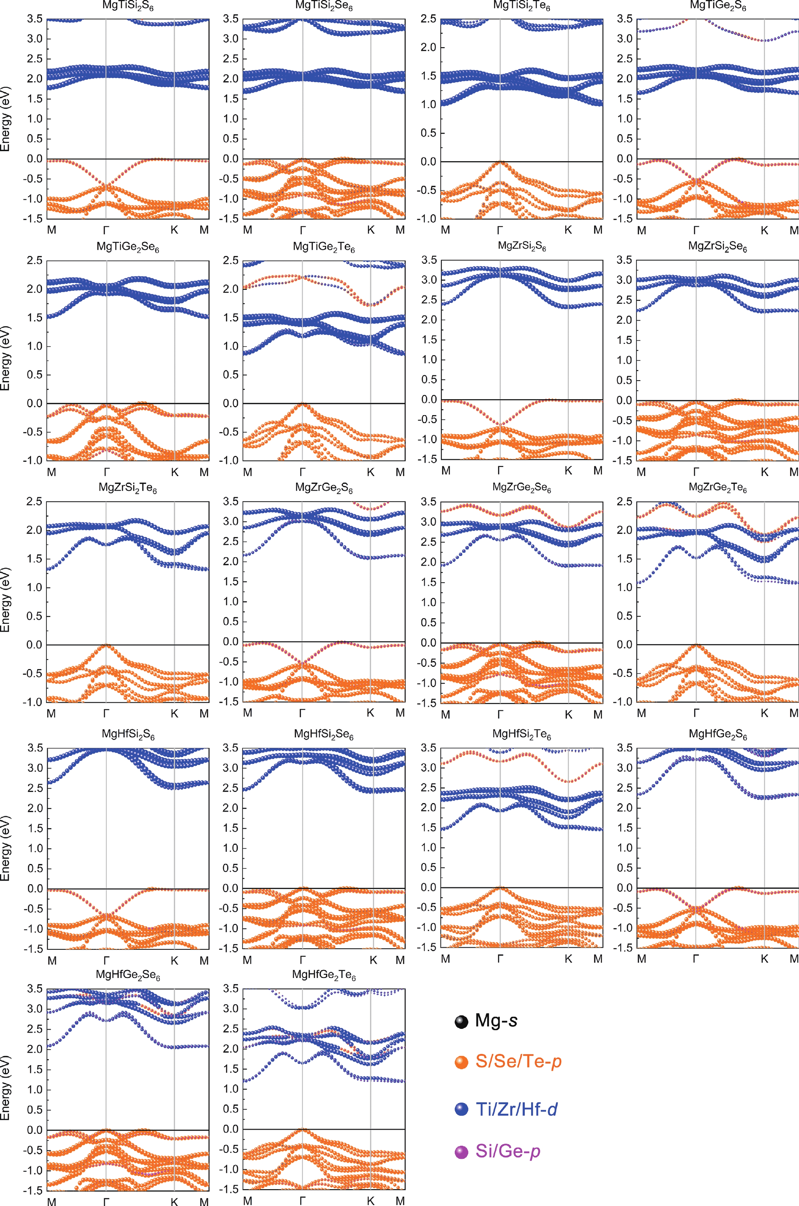
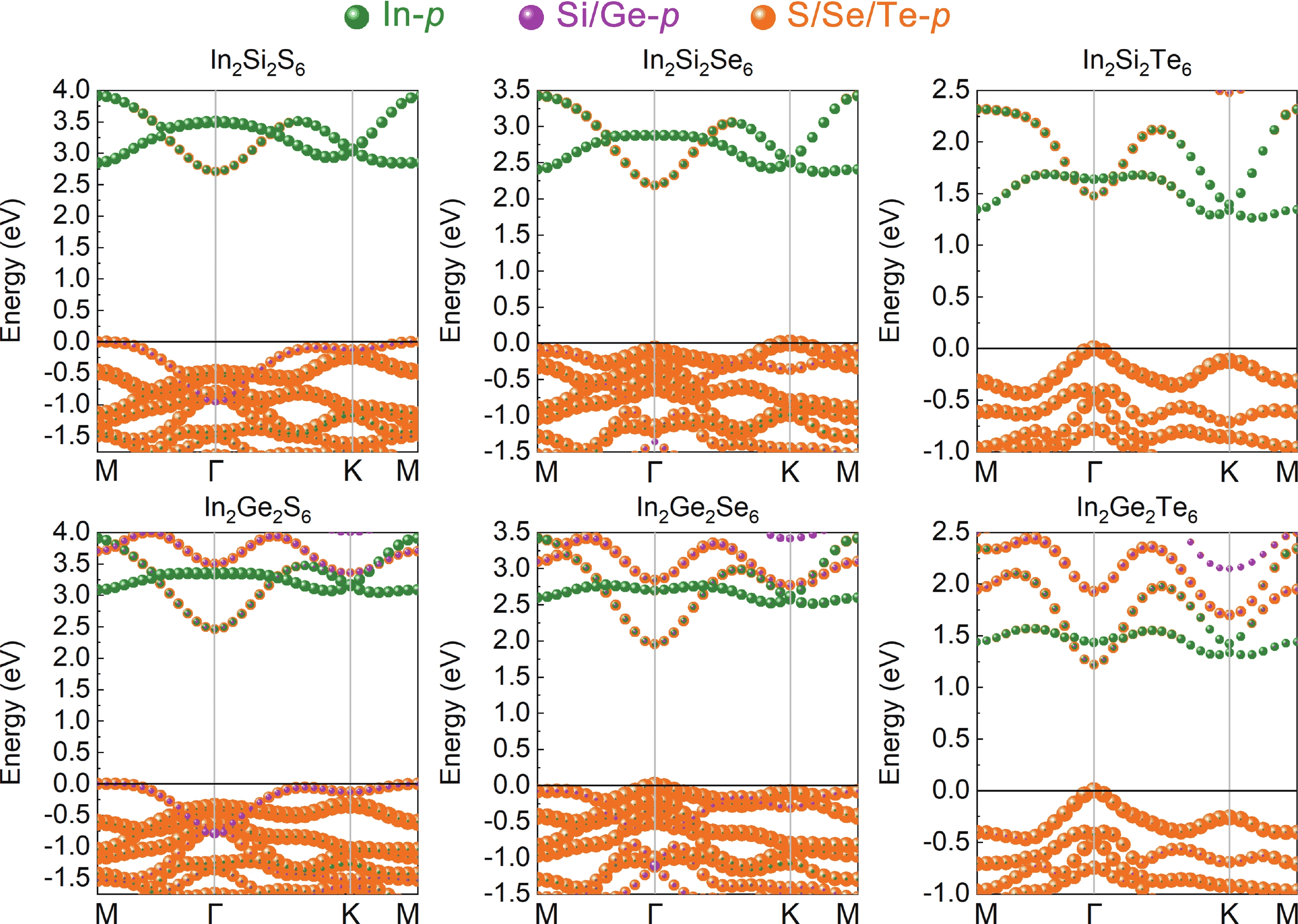
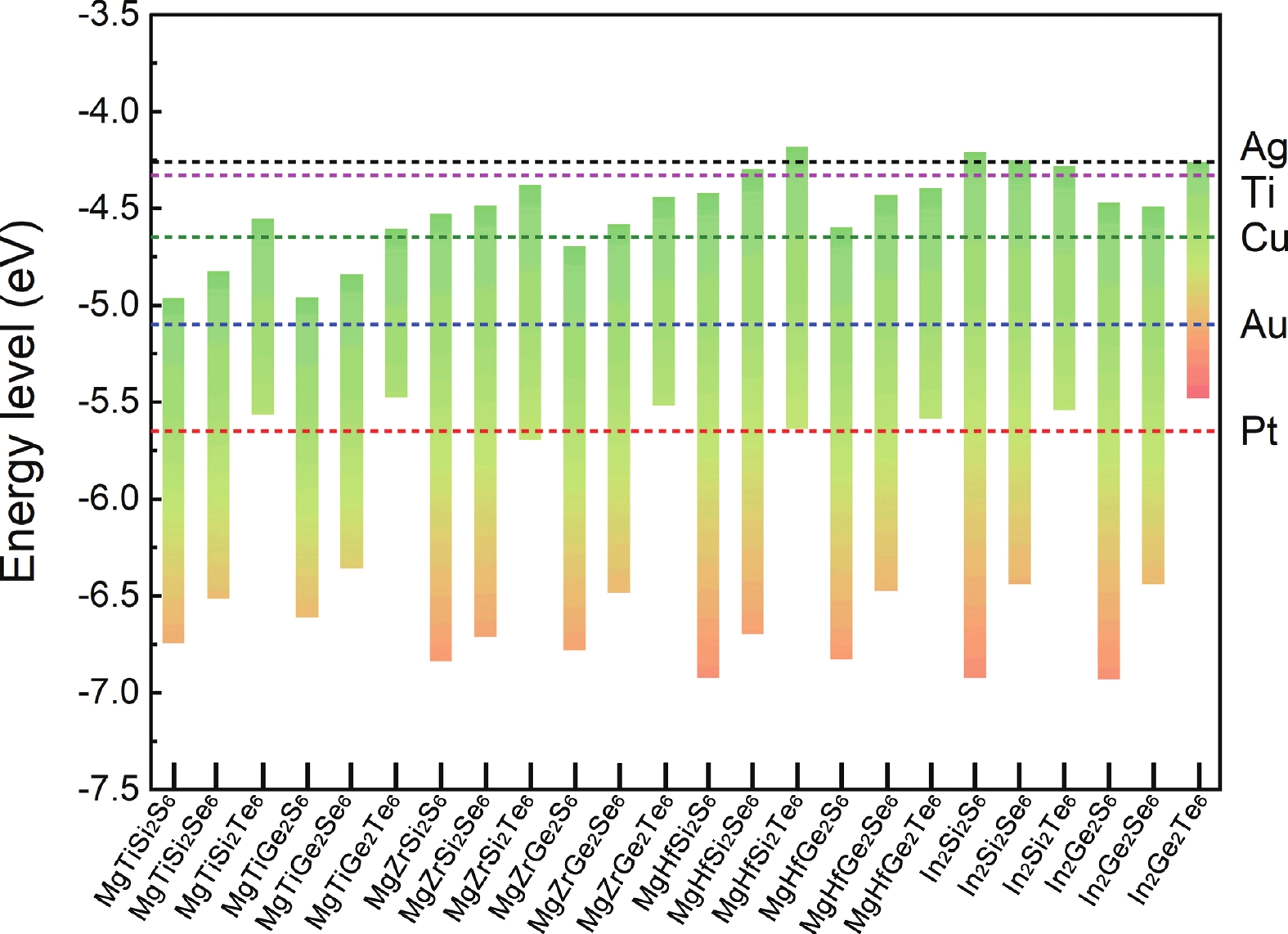
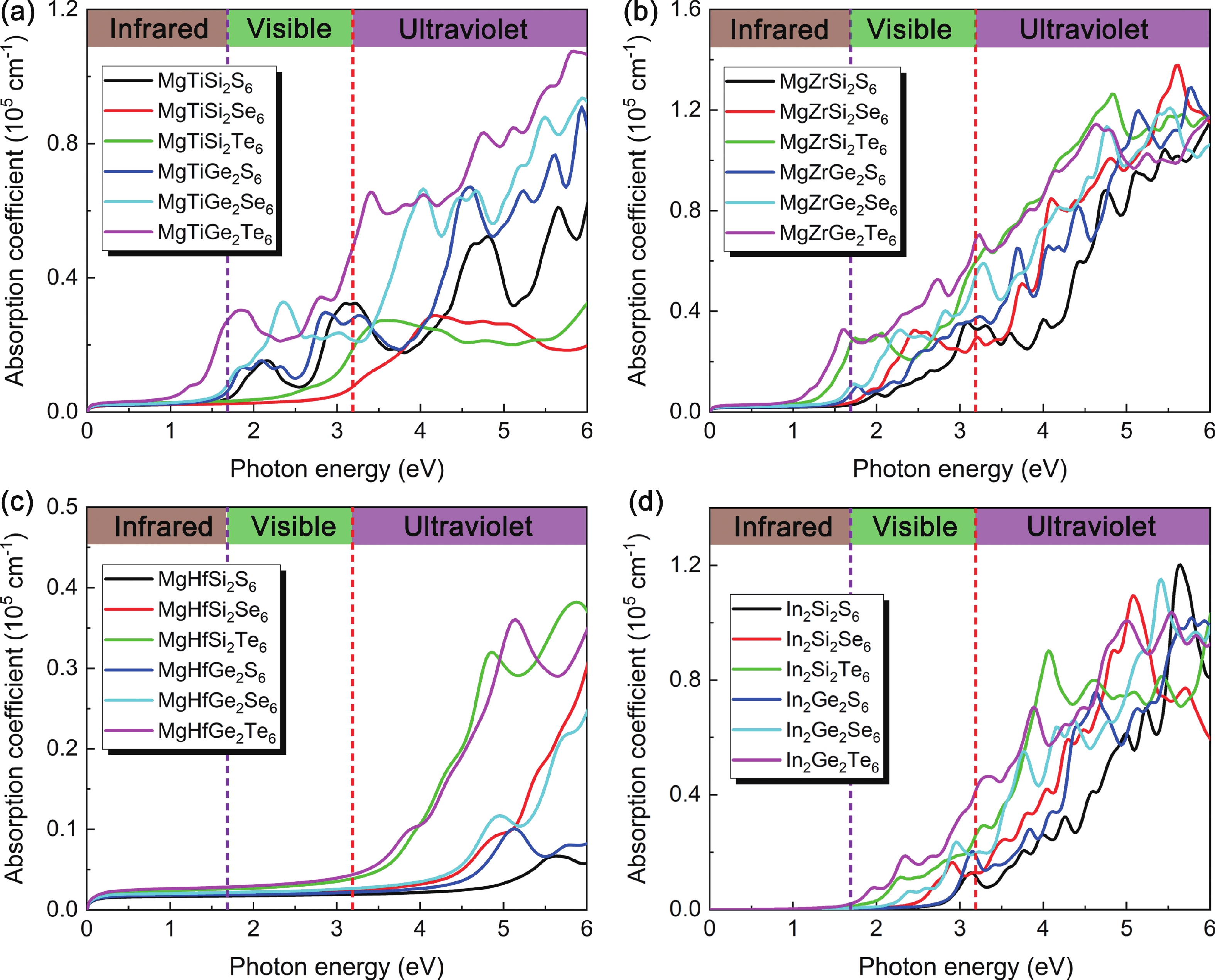
Inspired by the recently predicted 2D MX2Y6 (M = metal element; X = Si/Ge/Sn; Y = S/Se/Te), we explore the possible applications of alkaline earth metal (using magnesium as example) in this family based on the idea of element replacement and valence electron balance. Herein, we report a new family of 2D quaternary compounds, namely MgMX2Y6 (M = Ti/Zr/Hf; X = Si/Ge; Y = S/Se/Te) monolayers, with superior kinetic, thermodynamic and mechanical stability. In addition, our results indicate that MgMX2Y6 monolayers are all indirect band gap semiconductors with band gap values ranging from 0.870 to 2.500 eV. Moreover, the band edges and optical properties of 2D MgMX2Y6 are suitable for constructing multifunctional optoelectronic devices. Furthermore, for comparison, the mechanical, electronic and optical properties of In2X2Y6 monolayers have been discussed in detail. The success of introducing Mg into the 2D MX2Y6 family indicates that more potential materials, such as Ca- and Sr-based 2D MX2Y6 monolayers, may be discovered in the future. Therefore, this work not only broadens the existing family of 2D semiconductors, but it also provides beneficial results for the future.
J. Semicond.
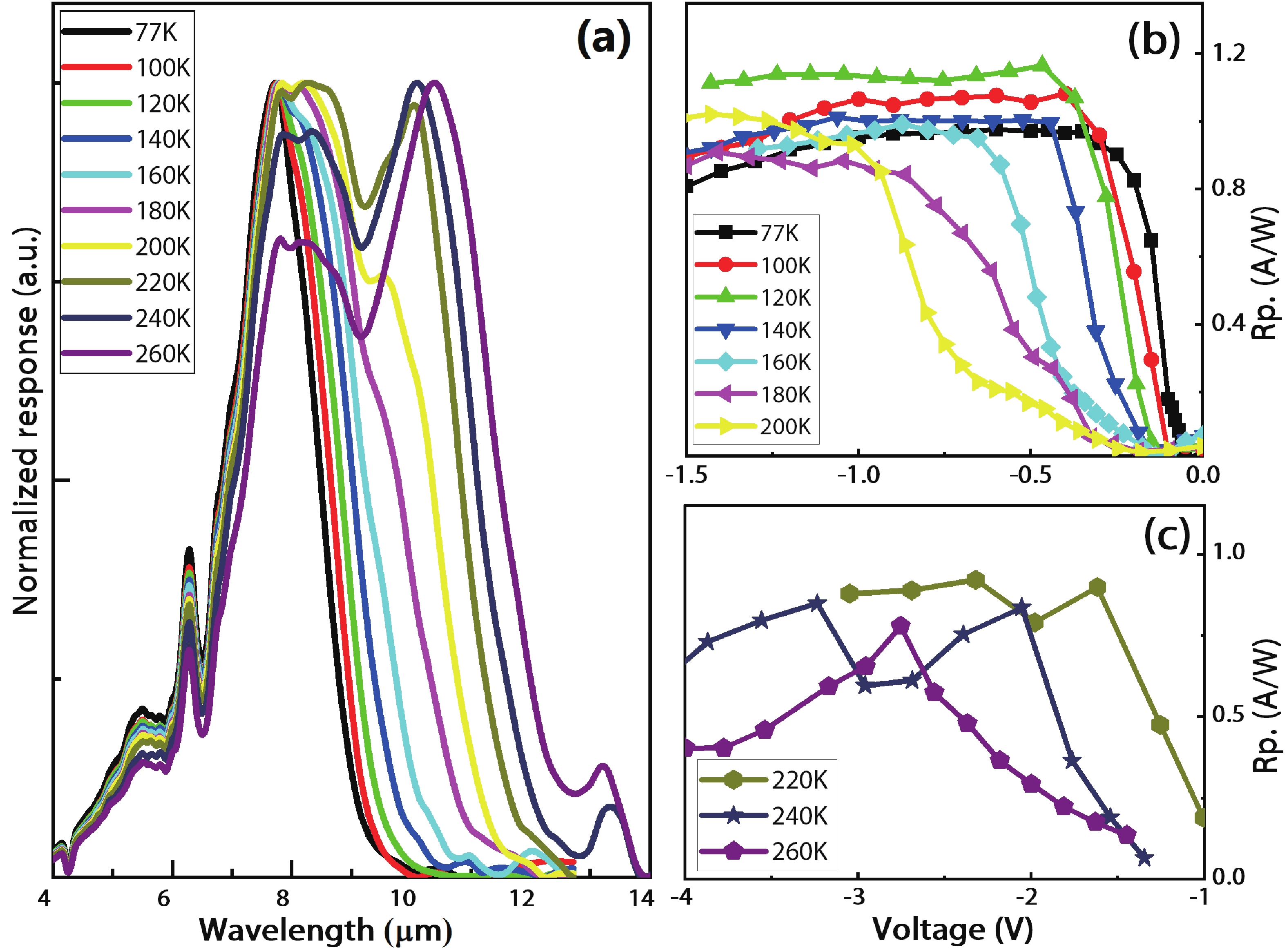
2023, 44(4): 042301 doi: 10.1088/1674-4926/44/4/042301
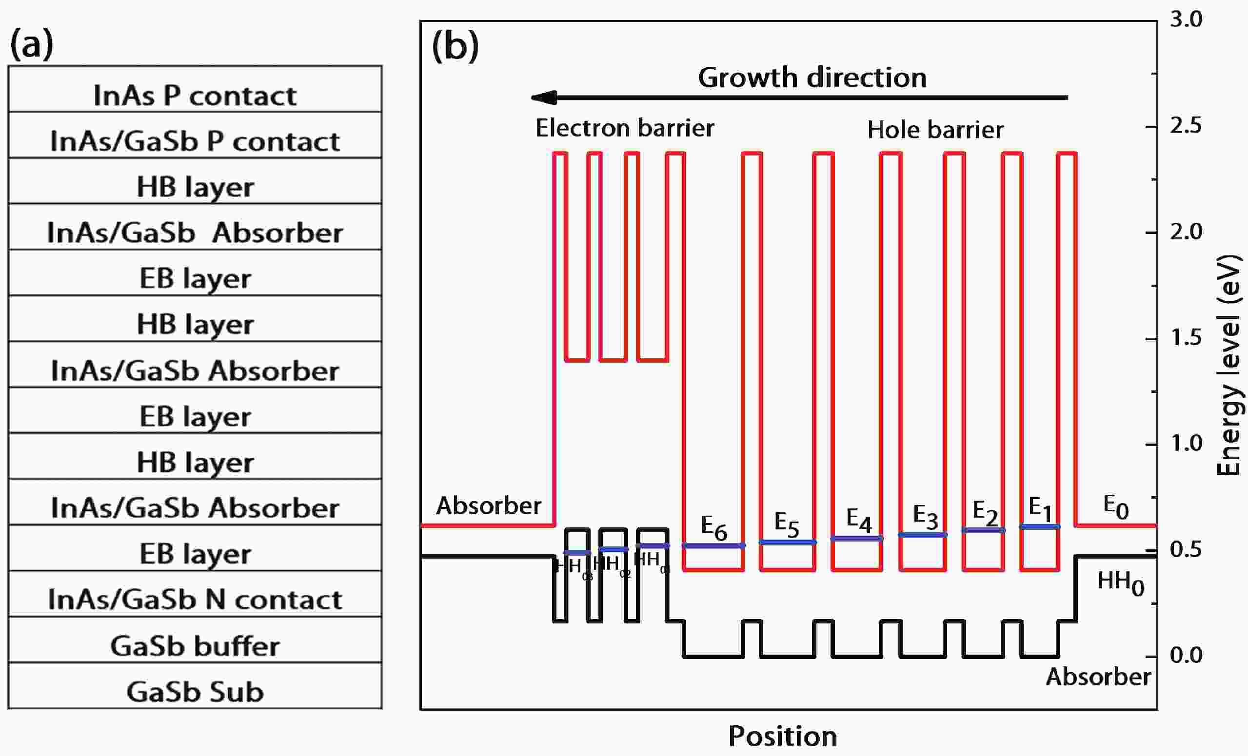
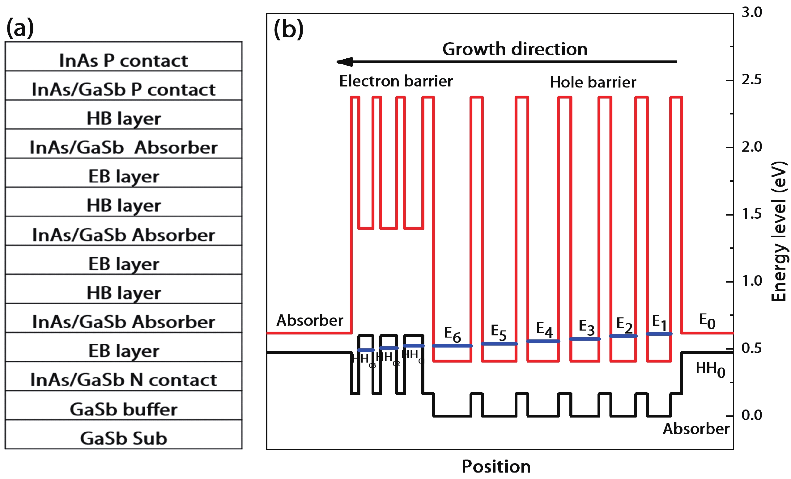
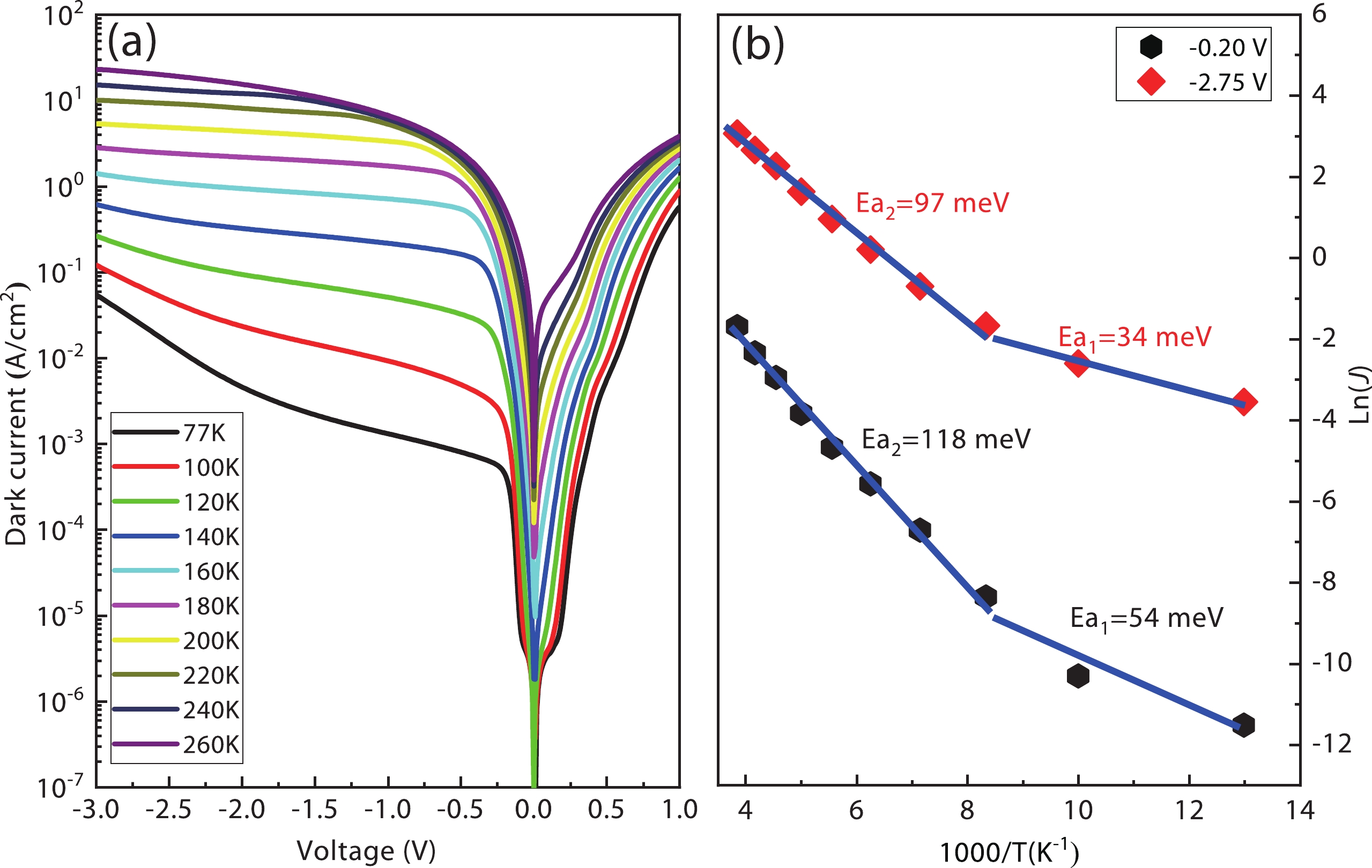
We report on a long wavelength interband cascade photodetector with type II InAs/GaSb superlattice absorber. The device is a three-stage interband cascade structure. At 77 K, the 50% cutoff wavelength of the detector is 8.48 μm and the peak photoresponse wavelength is 7.78 μm. The peak responsivity is 0.93 A/W and the detectivity D* is 1.12 × 1011 cm·Hz0.5/W for 7.78 μm at –0.20 V. The detector can operate up to about 260 K. At 260 K, the 50% cutoff wavelength is 11.52 μm, the peak responsivity is 0.78 A/W and the D* is 5.02 × 108 cm·Hz0.5/W for the peak wavelength of 10.39 μm at –2.75 V. The dark current of the device is dominated by the diffusion current under both a small bias voltage of –0.2 V and a large one of –2.75 V for the temperature range of 120 to 260 K.

J. Semicond.
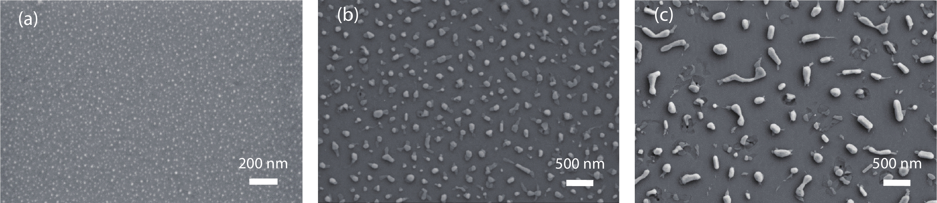
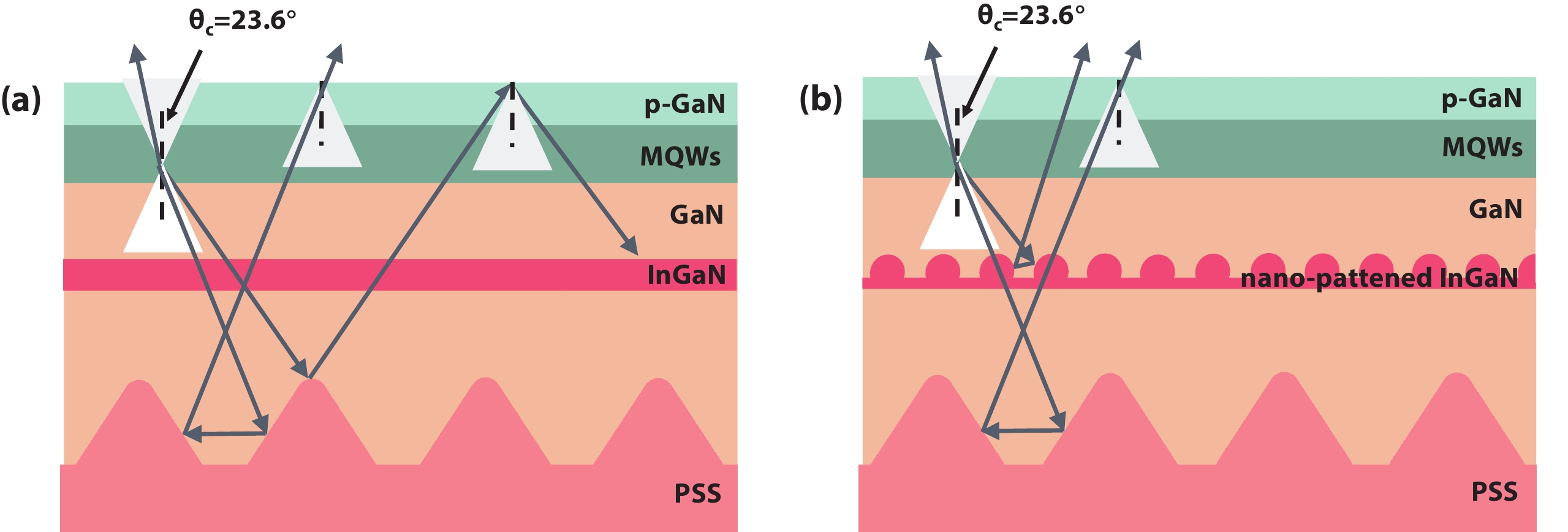
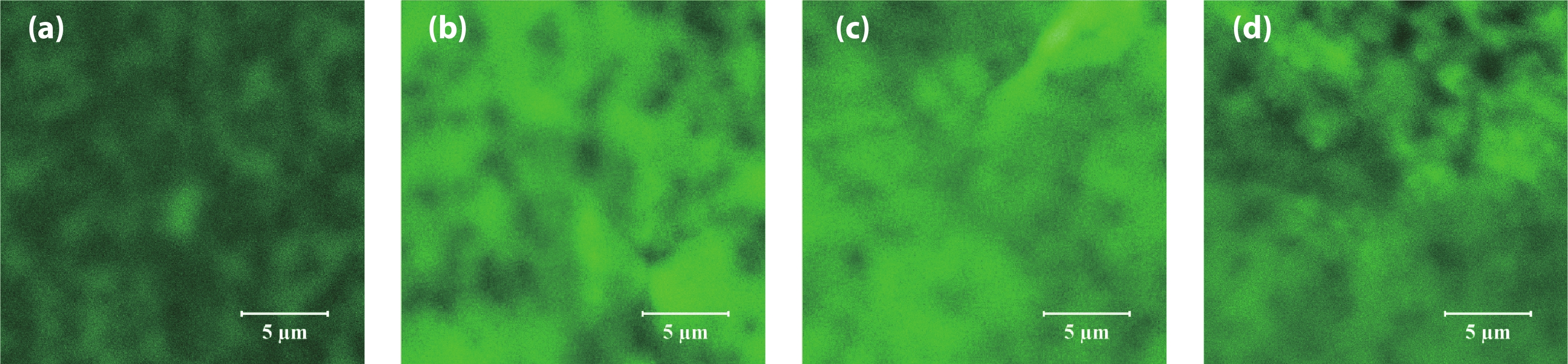
2023, 44(4): 042801 doi: 10.1088/1674-4926/44/4/042801
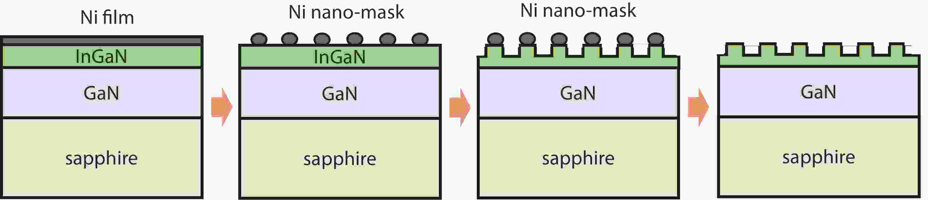
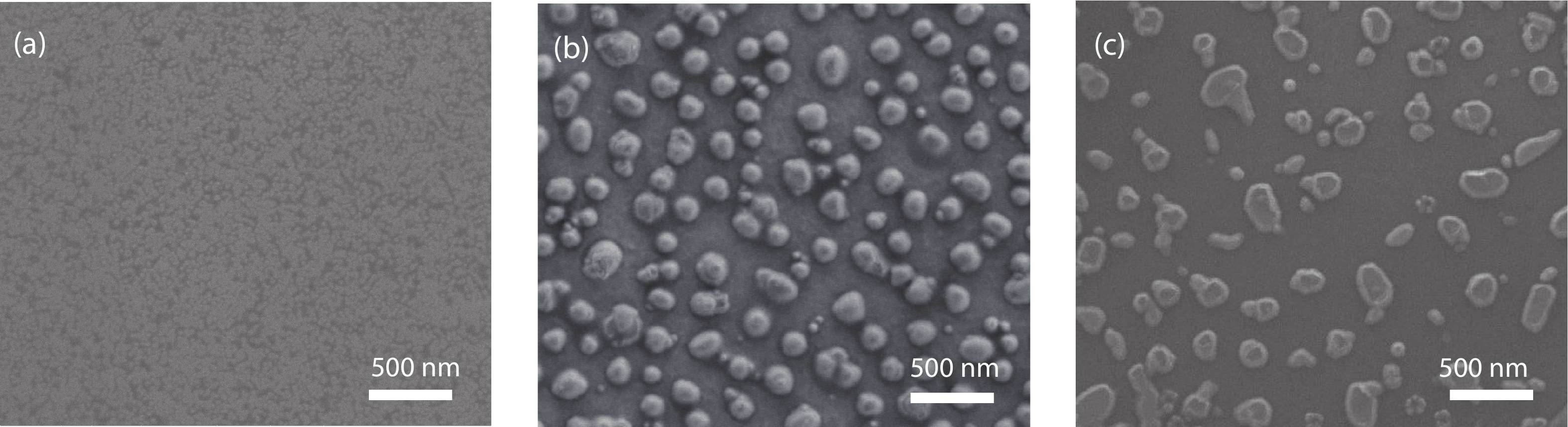
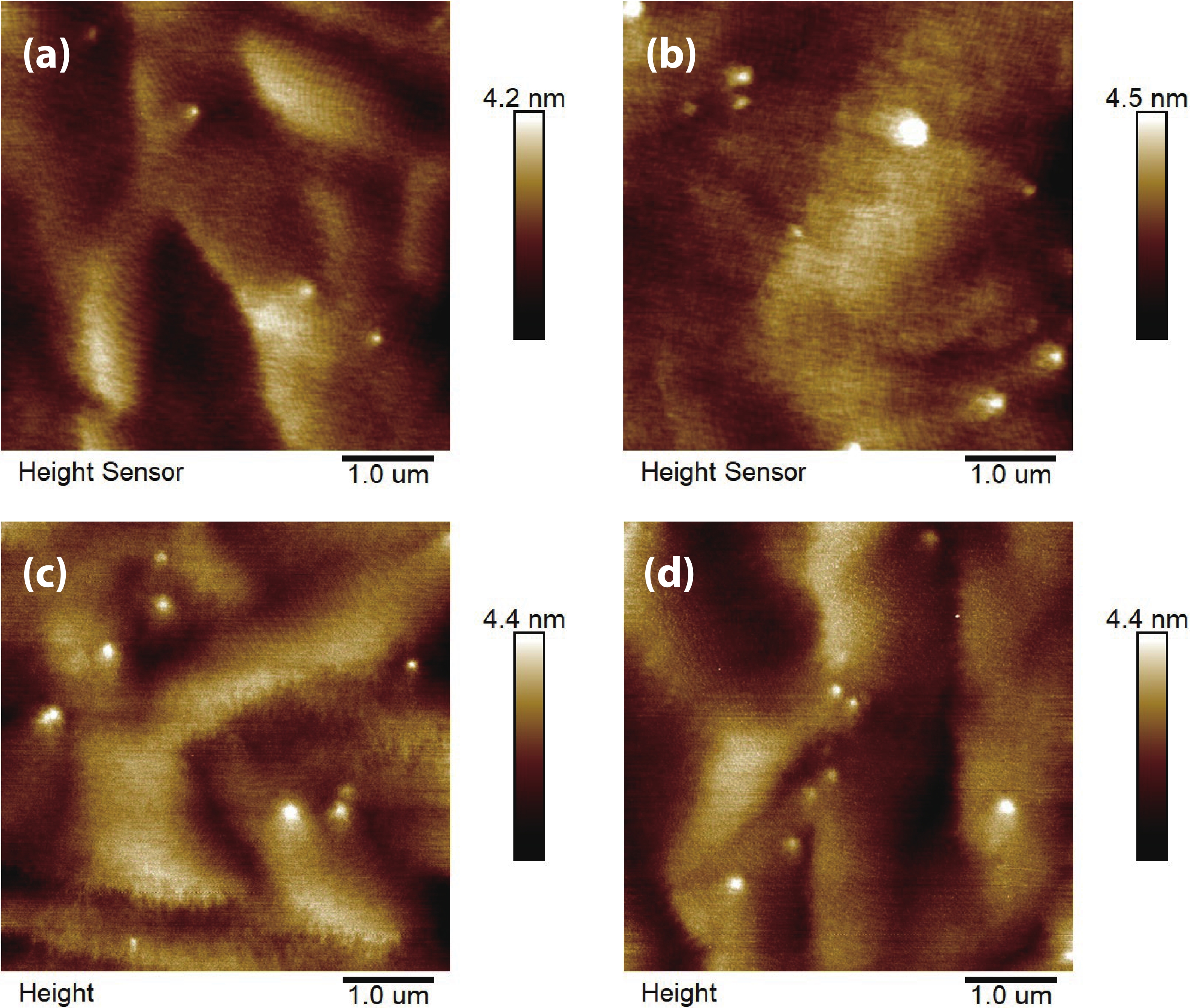
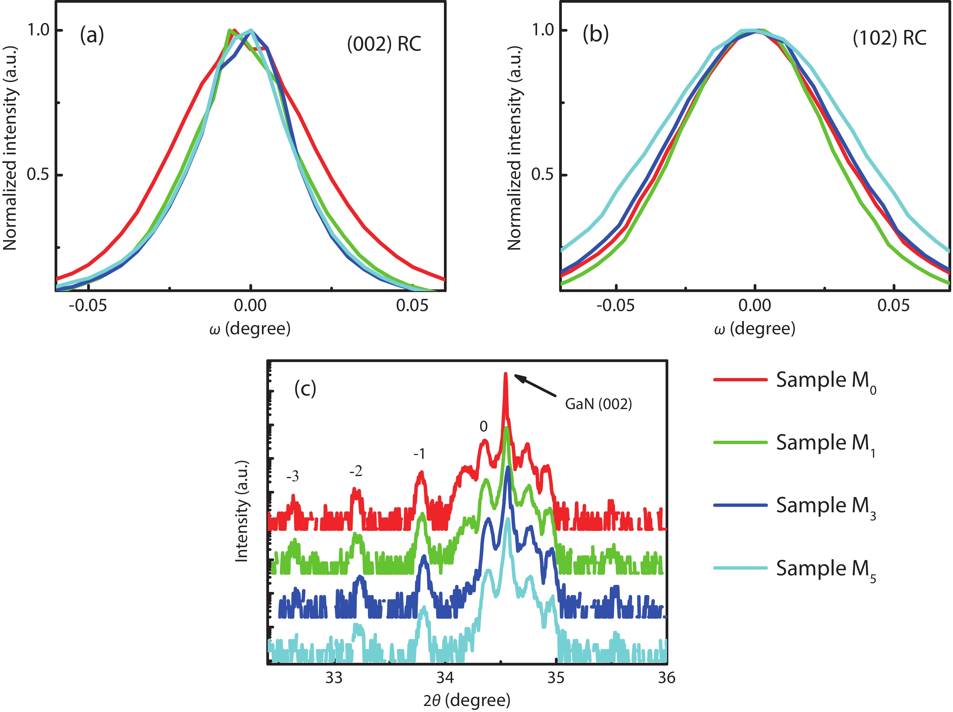
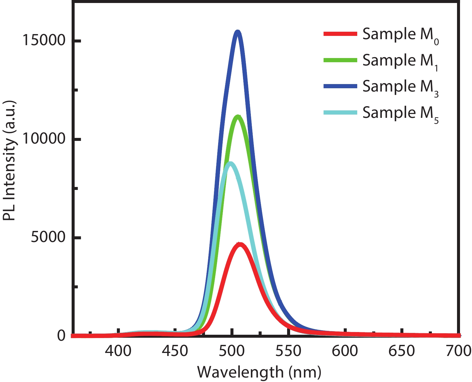
The nano-patterned InGaN film was used in green InGaN/GaN multiple quantum wells (MQWs) structure, to relieve the unpleasantly existing mismatch between high indium content InGaN and GaN, as well as to enhance the light output. The different self-assembled nano-masks were formed on InGaN by annealing thin Ni layers of different thicknesses. Whereafter, the InGaN films were etched into nano-patterned films. Compared with the green MQWs structure grown on untreated InGaN film, which on nano-patterned InGaN had better luminous performance. Among them the MQWs performed best when 3 nm thick Ni film was used as mask, because that optimally balanced the effects of nano-patterned InGaN on the crystal quality and the light output.
J. Semicond.
2023, 44(4): 042802 doi: 10.1088/1674-4926/44/4/042802
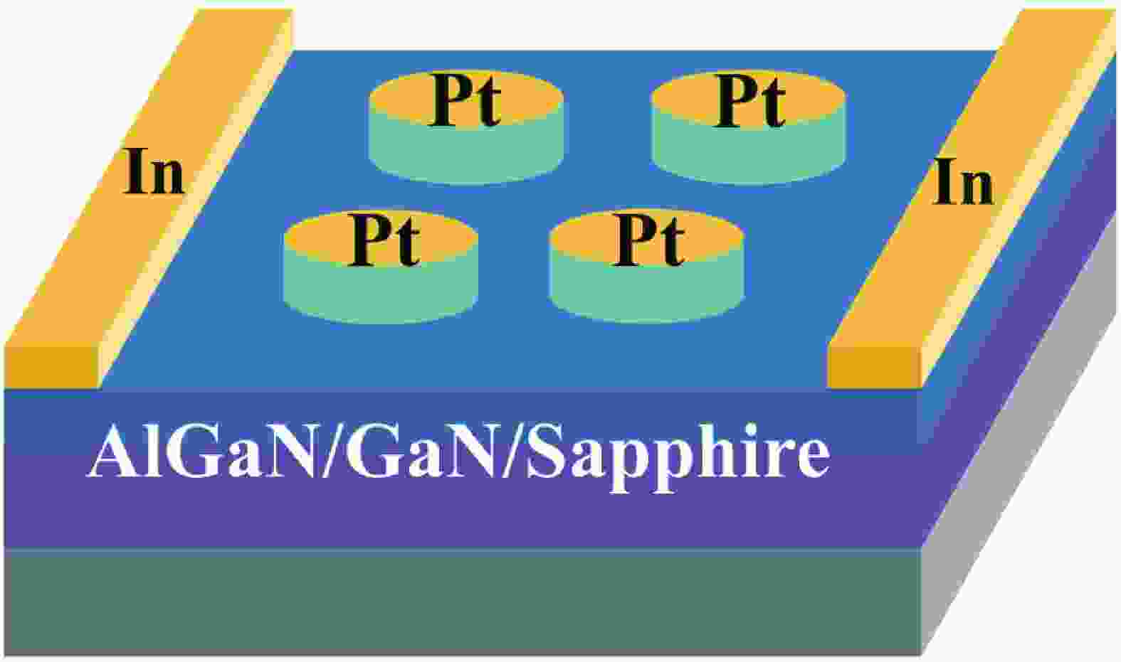
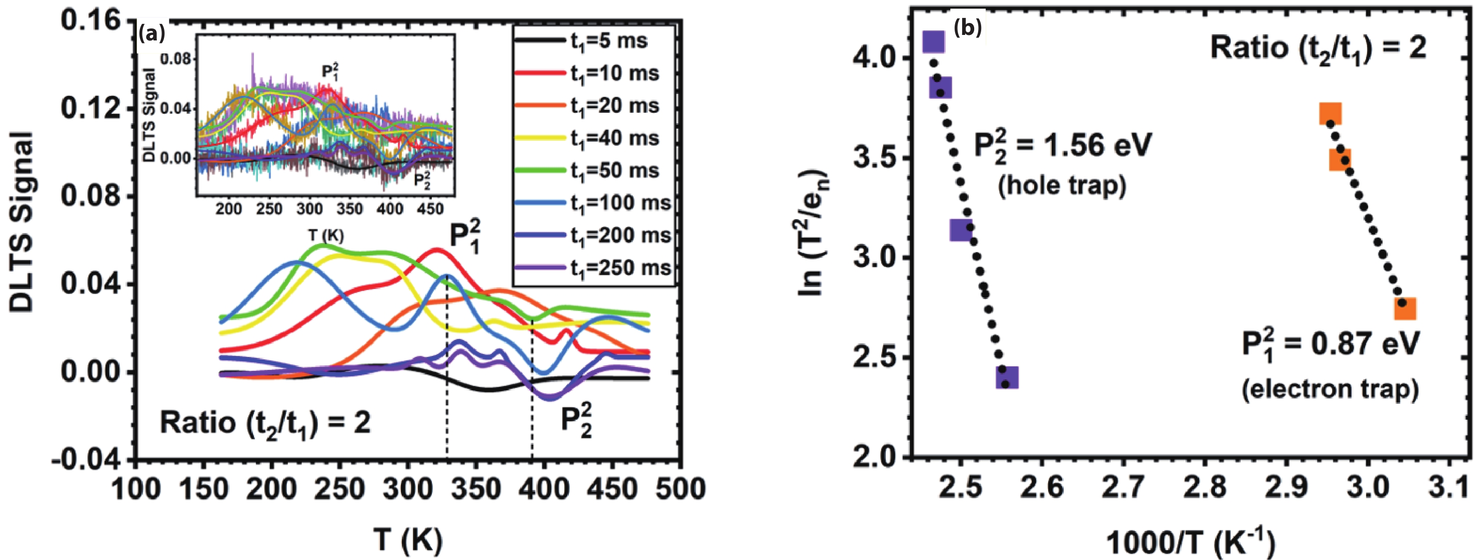
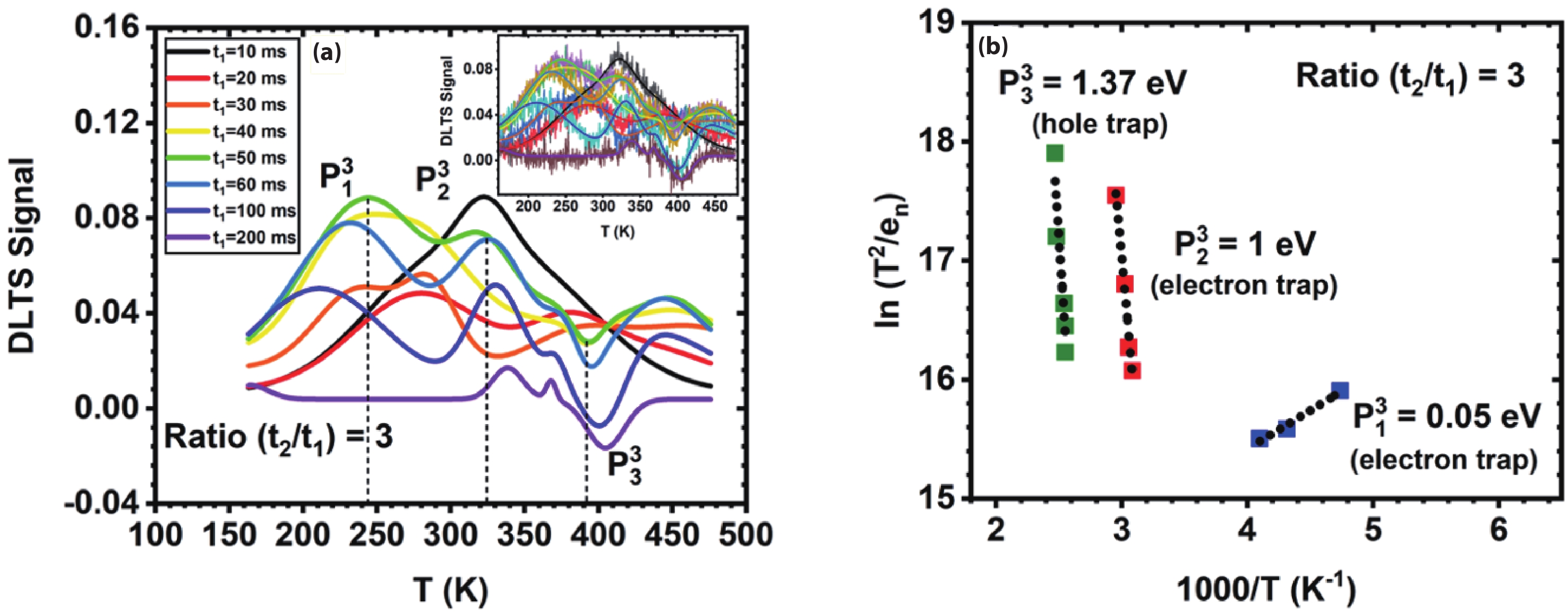
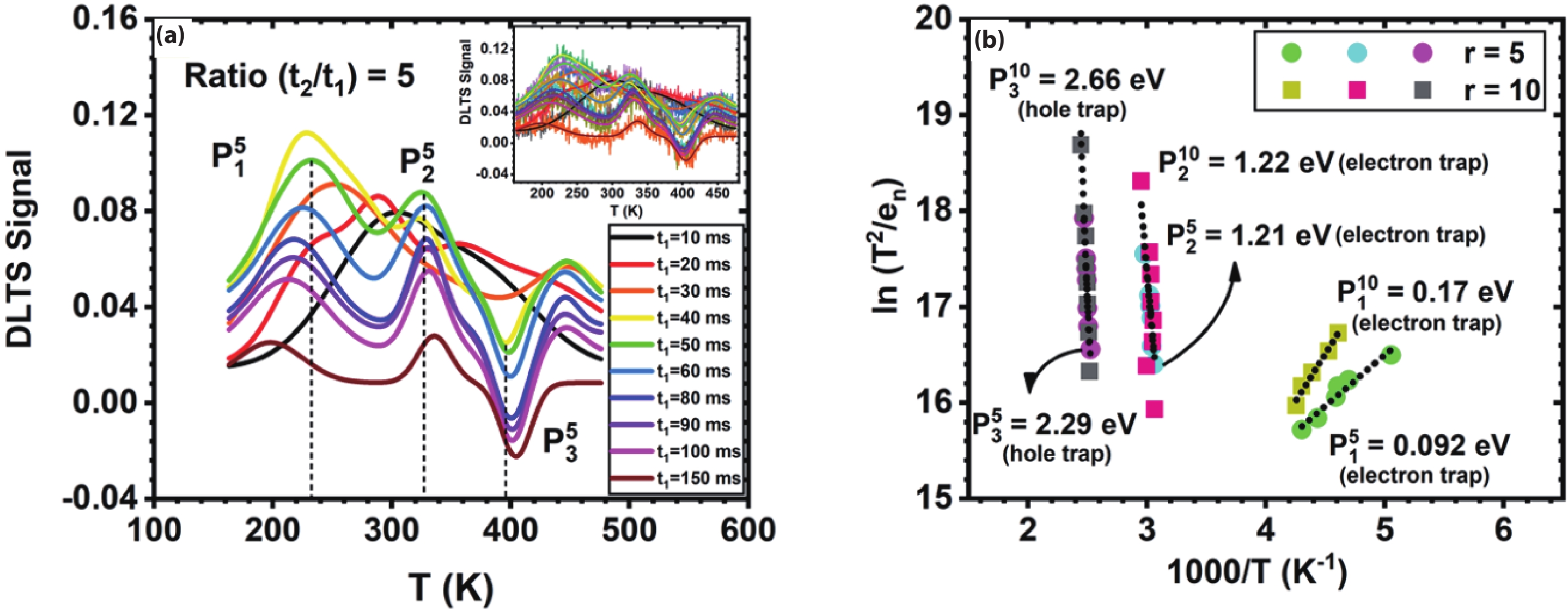
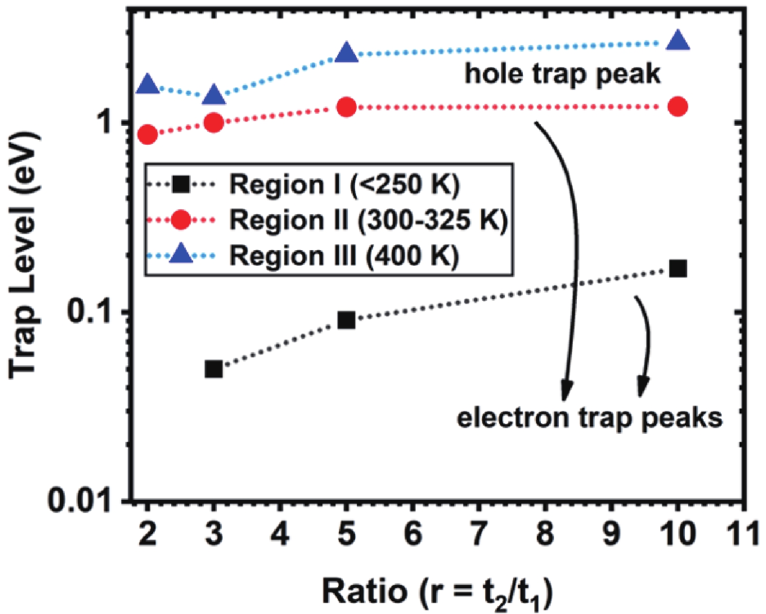
Trap characterization on GaN Schottky barrier diodes (SBDs) has been carried out using deep-level transient spectroscopy (DLTS). Selective probing by varying the ratio of the rate window values (r) incites different trap signatures at similar temperature regimes. Electron traps are found to be within the values: 0.05–1.2 eV from the conduction band edge whereas the hole traps 1.37–2.66 eV from the valence band edge on the SBDs. In the lower temperature regime, the deeper electron traps contribute to the capacitance transients with increasing r values, whereas at the higher temperatures >300 K, a slow variation of the trap levels (both electrons and holes) is observed when r is varied. These traps are found to be mainly contributed to dislocations, interfaces, and vacancies within the structure.

J. Semicond.
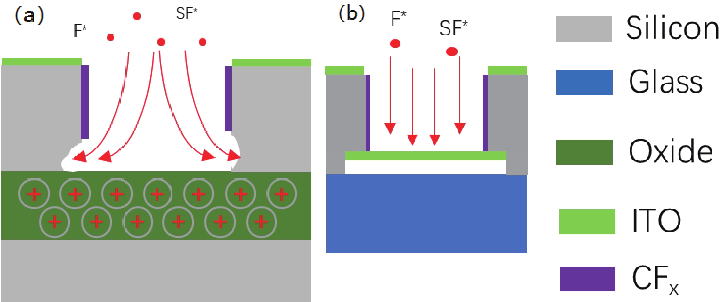
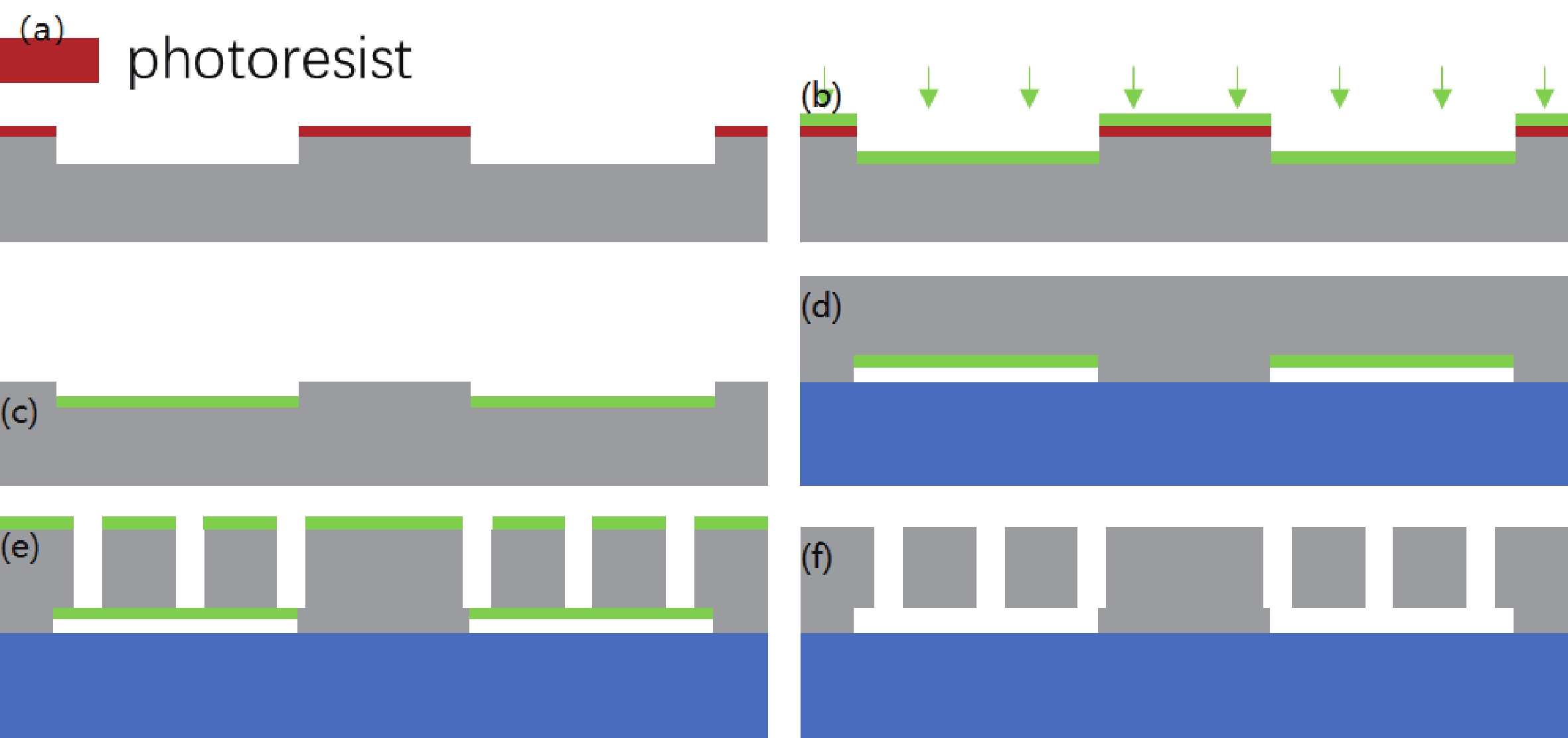
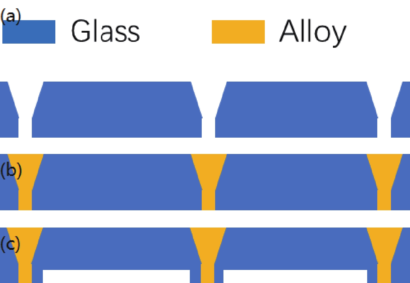
2023, 44(4): 044101 doi: 10.1088/1674-4926/44/4/044101
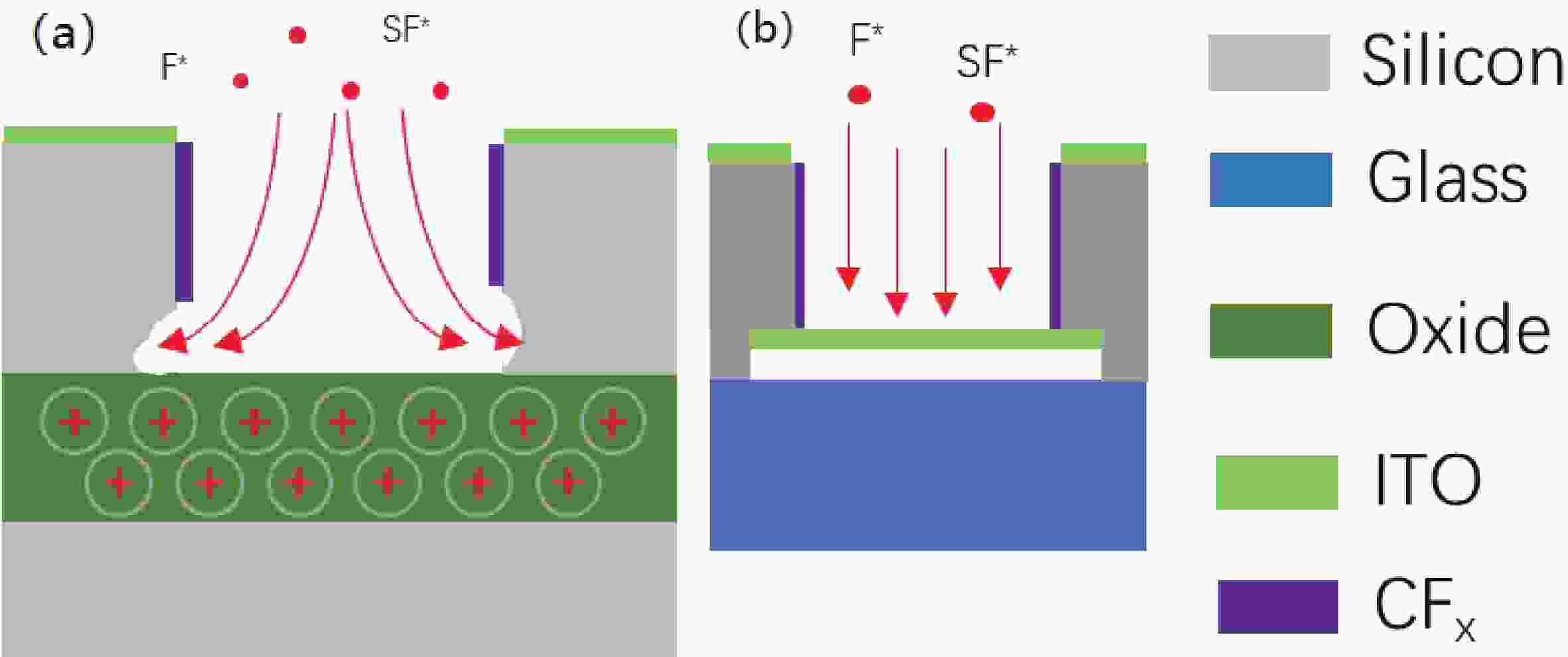
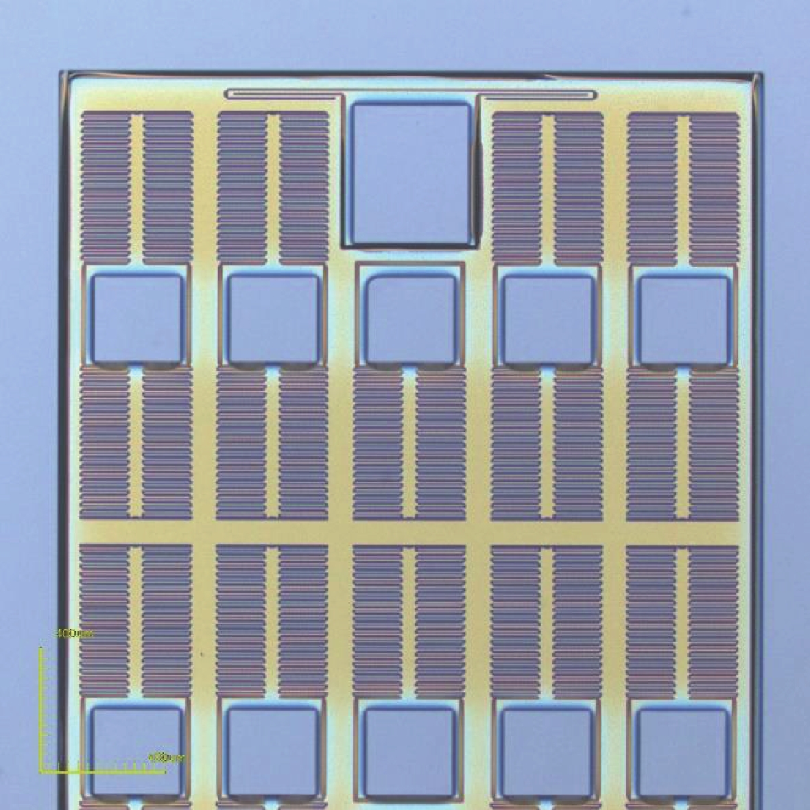
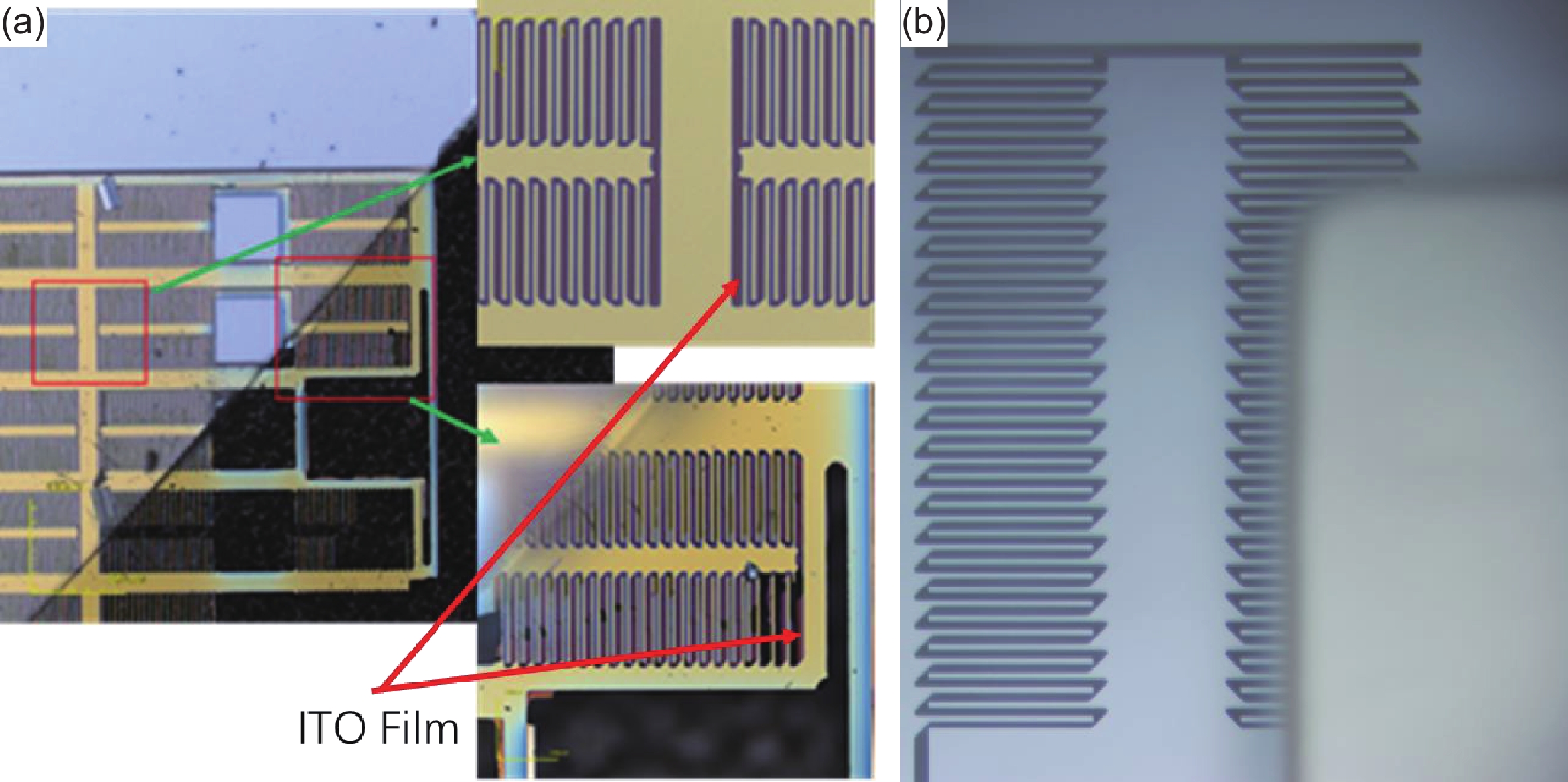
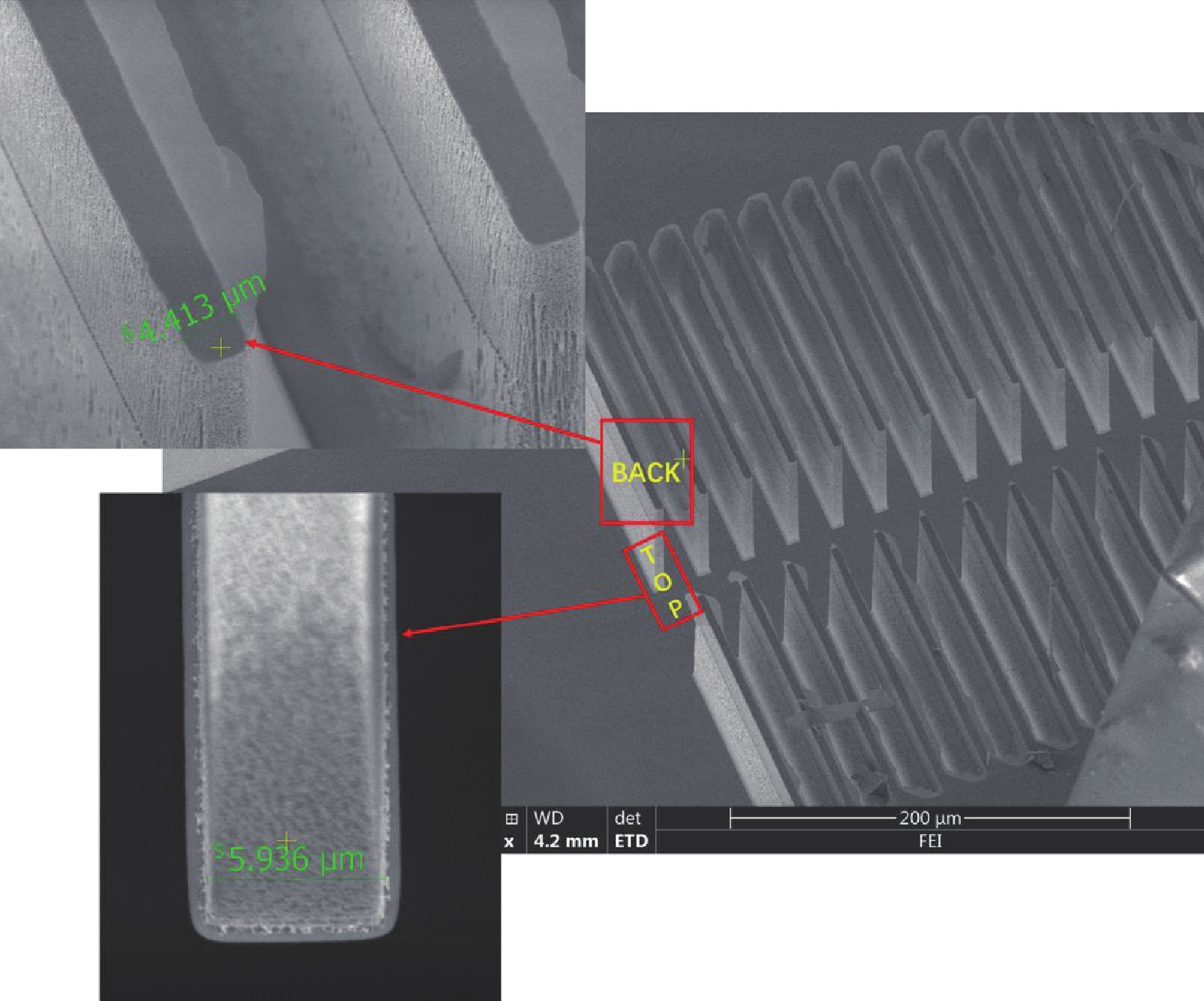
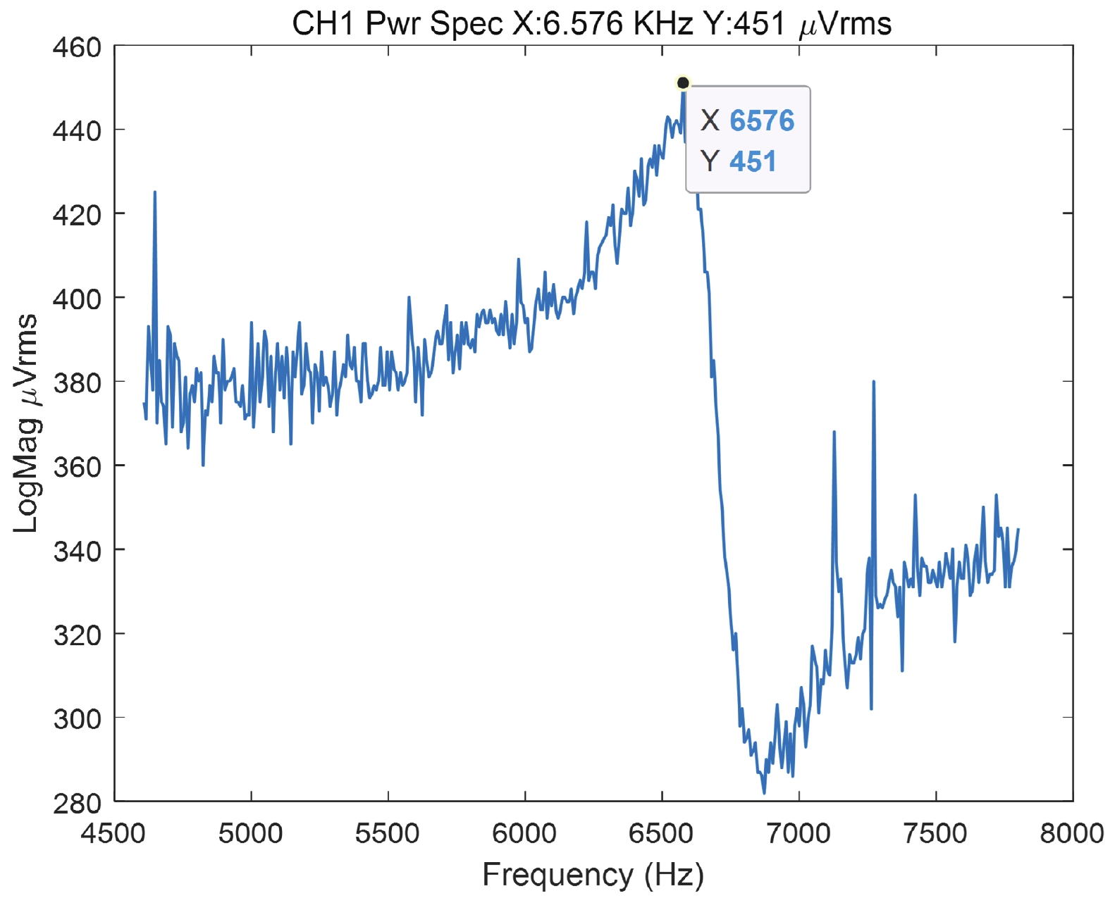
The silicon on glasses process is a common preparation method of micro-electro-mechanical system inertial devices, which can realize the processing of thick silicon structures. This paper proposes that indium tin oxides (ITO) film can serve as a deep silicon etching cut-off layer because ITO is less damaged under the attack of fluoride ions. ITO has good electrical conductivity and can absorb fluoride ions for silicon etching and reduce the reflection of fluoride ions, thus reducing the foot effect. The removal and release of ITO use an acidic solution, which does not damage the silicon structure. Therefore, the selection of the sacrificial layer has an excellent effect in maintaining the shape of the MEMS structure. This method is used in the preparation of MEMS accelerometers with a structure thickness of 100 μm and a feature size of 4 μm. The over-etching of the bottom of the silicon structure caused by the foot effect is negligible. The difference between the simulated value and the designed value of the device characteristic frequency is less than 5%. This indicates that ITO is an excellent deep silicon etch stopper material.


J. Semicond.
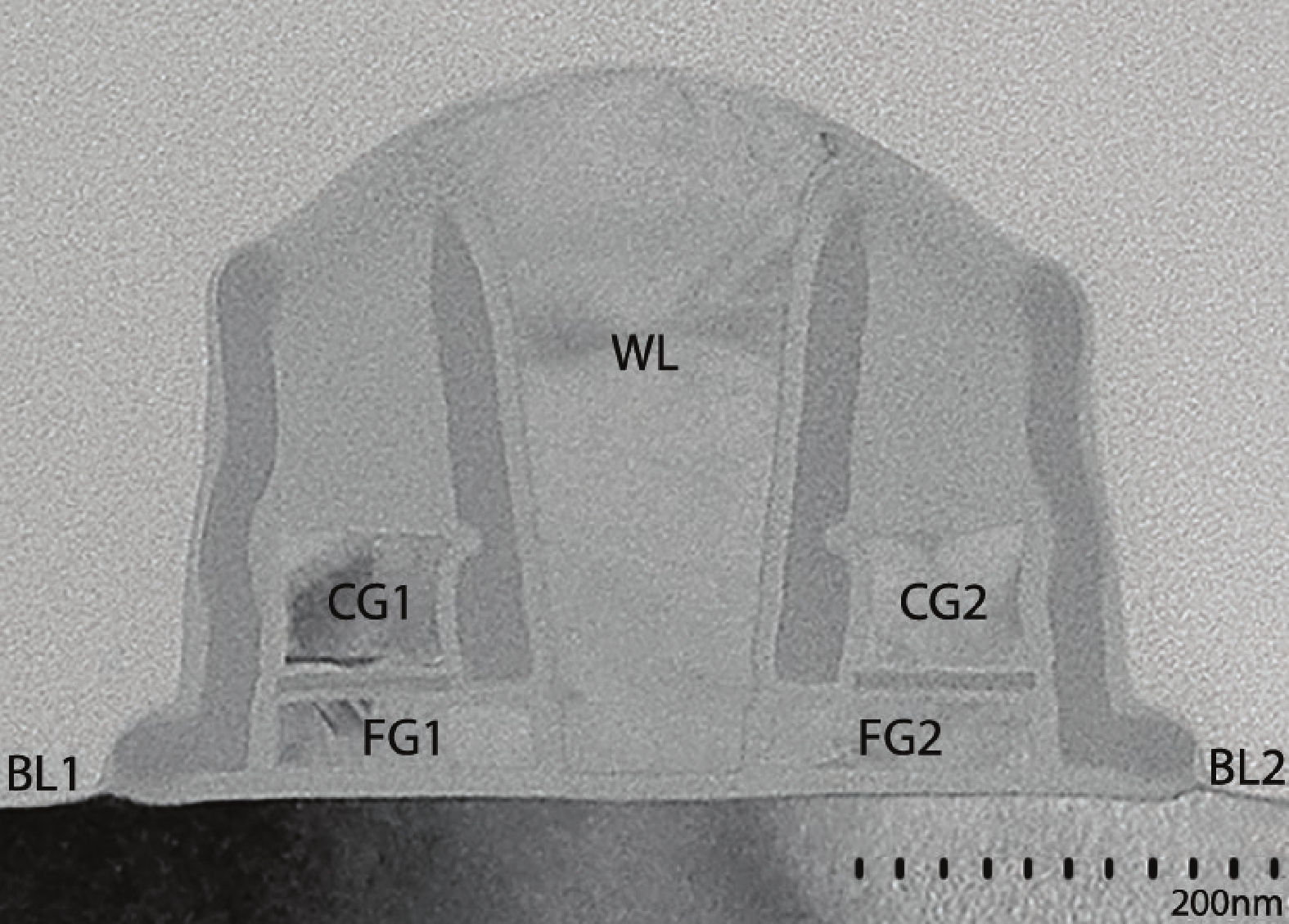
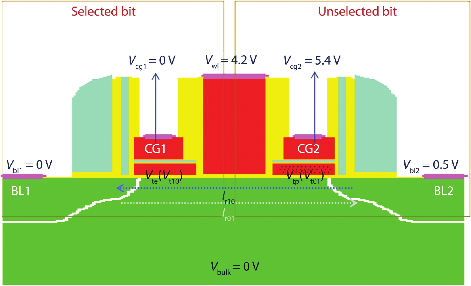
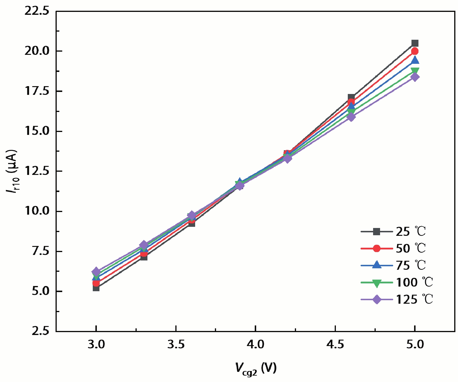
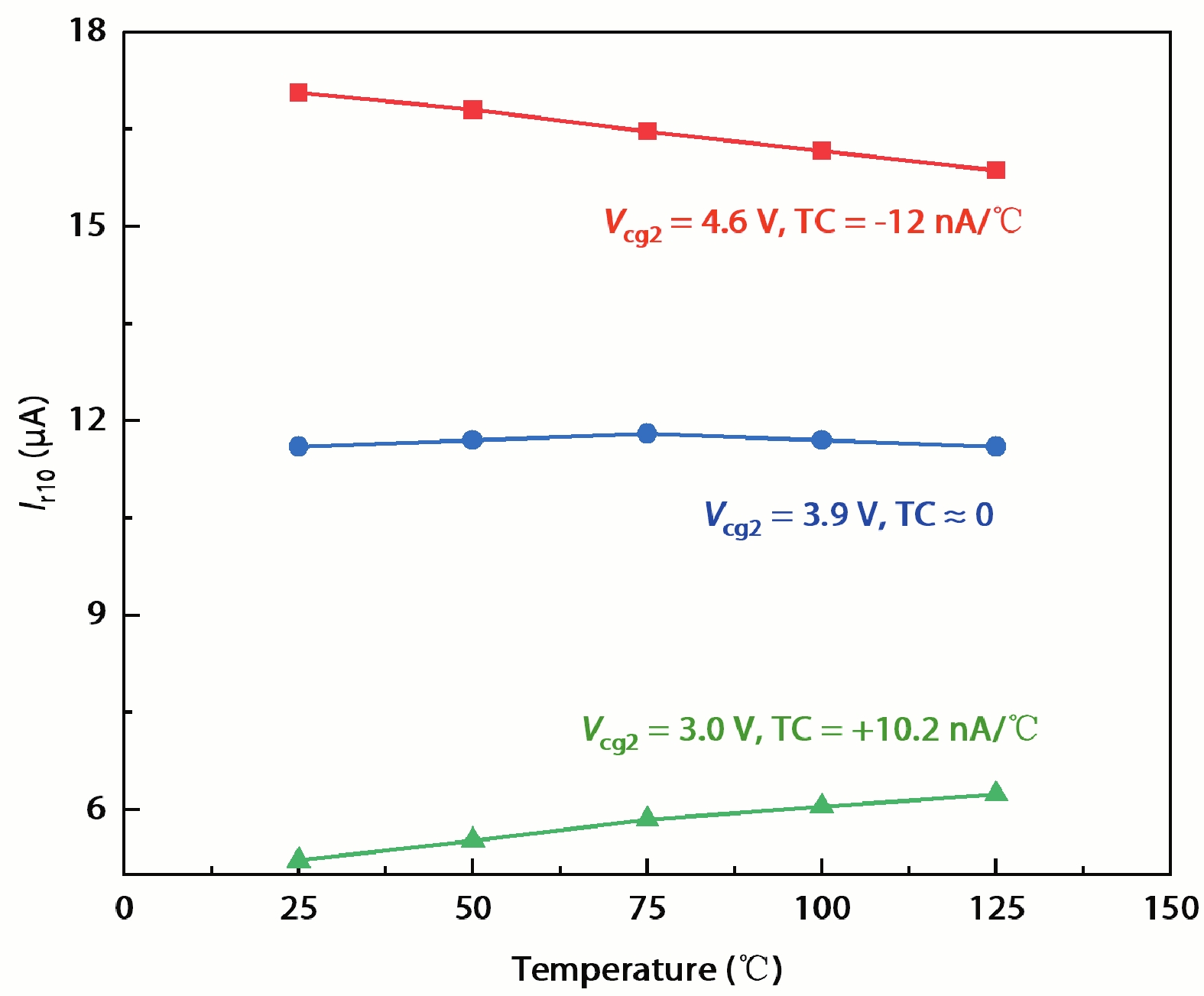
2023, 44(4): 044102 doi: 10.1088/1674-4926/44/4/044102
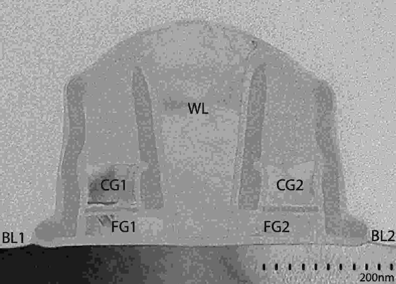
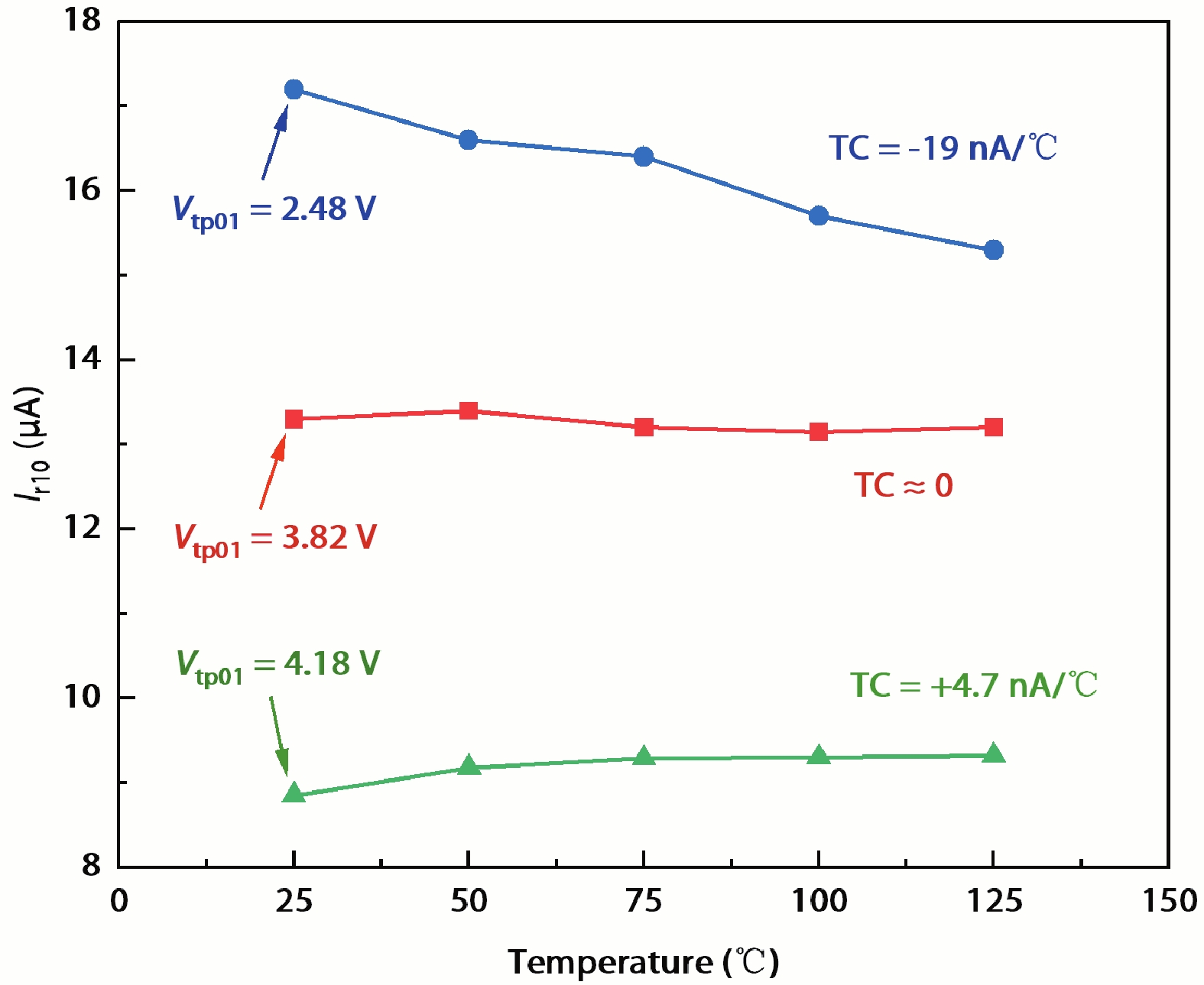
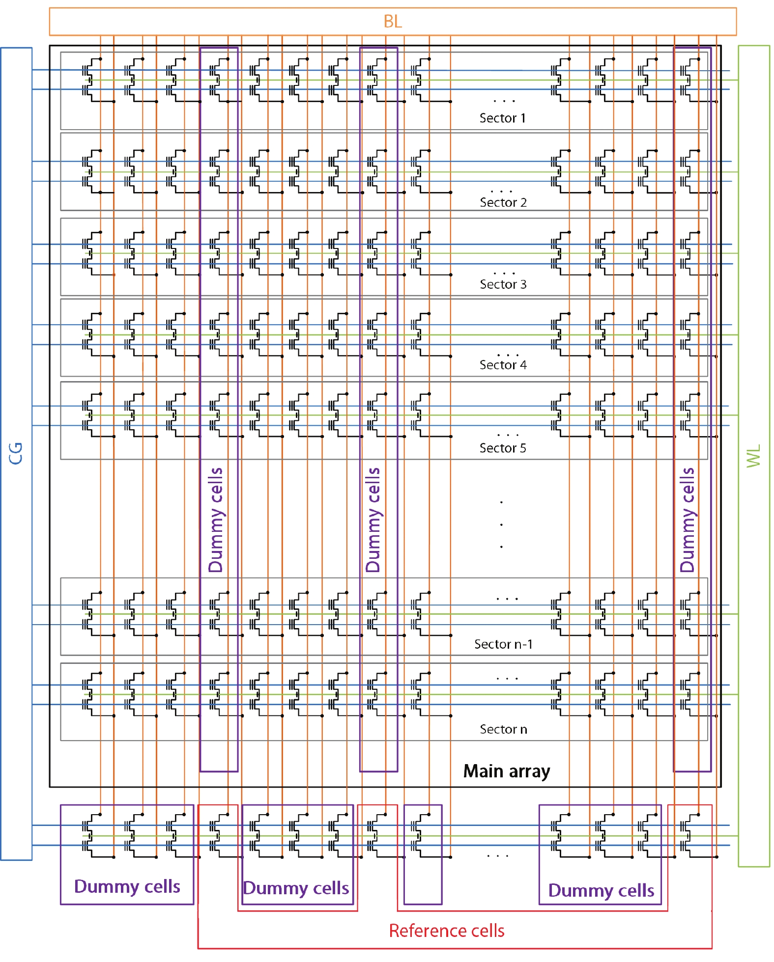
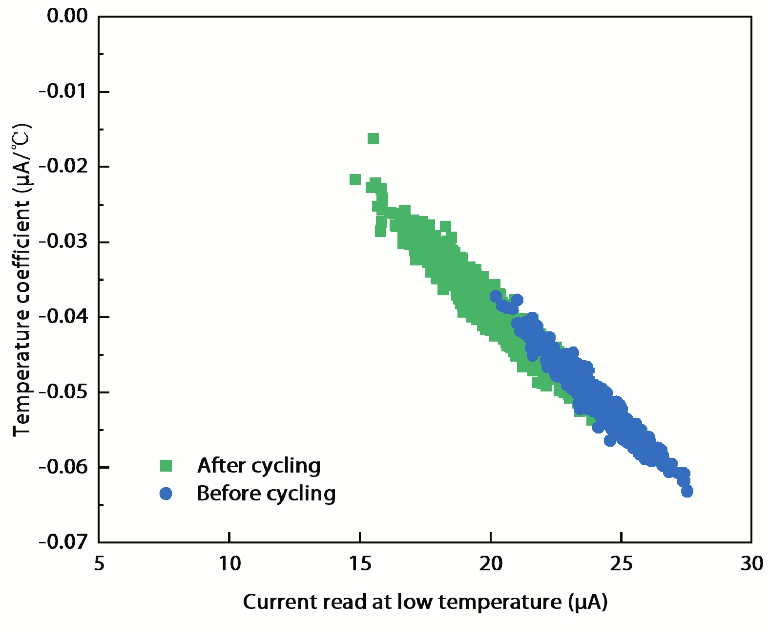
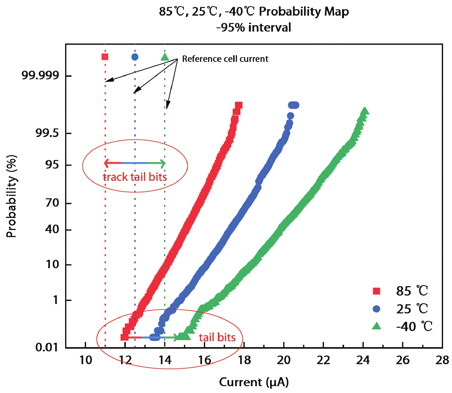
The temperature characteristics of the read current of the NOR embedded flash memory with a 1.5T-per-cell structure are theoretically analyzed and experimentally verified. We verify that for a cell programmed with a “10” state, the read current is either increasing, decreasing, or invariable with the temperature, essentially depending on the reading overdrive voltage of the selected bitcell, or its programming strength. By precisely controlling the programming strength and thus manipulating its temperature coefficient, we propose a new setting method for the reference cells that programs each of reference cells to a charge state with a temperature coefficient closely tracking tail data cells, thereby solving the current coefficient mismatch and improving the read window.