J. Semicond. >  In Press >  doi: 10.1088/1674-4926/23120006

ARTICLES

Recess-free enhancement-mode AlGaN/GaN RF HEMTs on Si substrate

Tiantian Luan1, 2, Sen Huang1, 2, , Guanjun Jing1, 2, Jie Fan1, 2, Haibo Yin1, 2, Xinguo Gao1, 2, Sheng Zhang1, 2, Ke Wei1, 2, Yankui Li1, 2, Qimeng Jiang1, 2, Xinhua Wang1, 2, Bin Hou3, Ling Yang3, Xiaohua Ma3 and Xinyu Liu1, 2

+ Author Affiliations

 Corresponding author: Sen Huang, huangsen@ime.ac.cn

PDF

Turn off MathJax

Abstract: Enhancement-mode (E-mode) GaN-on-Si radio-frequency (RF) high-electron-mobility transistors (HEMTs) were fabricated on an ultrathin-barrier (UTB) AlGaN (<6 nm)/GaN heterostructure featuring a naturally depleted 2-D electron gas (2DEG) channel. The fabricated E-mode HEMTs exhibit a relatively high threshold voltage (VTH) of +1.1 V with good uniformity. A maximum current/power gain cut-off frequency (fT/fMAX) of 31.3/99.6 GHz with a power added efficiency (PAE) of 52.47% and an output power density (Pout) of 1.0 W/mm at 3.5 GHz were achieved on the fabricated E-mode HEMTs with 1-µm gate and Au-free ohmic contact.

Key words: AlGaN/GaN heterostructureultrathin-barrierenhancement-moderadio-frequencypower added efficiencysilicon substrate


[1]
Chen K J, Häberlen O, Lidow A, et al. GaN-on-Si power technology: Devices and applications. IEEE Trans Electron Devices, 2017, 64, 779 doi: 10.1109/TED.2017.2657579
[2]
Zheng Z Y, Zhang L, Song W J, et al. Gallium nitride-based complementary logic integrated circuits. Nat Electron, 2021, 4, 595 doi: 10.1038/s41928-021-00611-y
[3]
Lu H, Hou B, Yang L, et al. High RF performance GaN-on-Si HEMTs with passivation implanted termination. IEEE Electron Device Lett, 2022, 43, 188 doi: 10.1109/LED.2021.3135703
[4]
Zeng Q M, Li X J, Zhou Z, et al. Investigation of undoped AlGaN/GaN microwave power HEMT. J Semicond, 2005, 26, 151
[5]
Chen T S, Zhang B, Ren C J, et al. 14W X-band AlGaN/GaN HEMT power MMICs. J Semicond, 2008, 29, 1027
[6]
Wang D F, Chen X J, Liu X Y. A Ku-band 3.4 W/mm power AlGaN/GaN HEMT on a sapphire substrate. J Semicond, 2010, 31, 024001 doi: 10.1088/1674-4926/31/2/024001
[7]
Hu Y S, Wang Y G, Wang W, et al. 11.2 W/mm power density AlGaN/GaN high electron-mobility transistors on a GaN substrate. J Semicond, 2024, 45, 012501 doi: 10.1088/1674-4926/45/1/012501
[8]
Wang Q, Chen C X, Li W, et al. Fabrication and characterization of AlGaN/GaN HEMTs with high power gain and efficiency at 8 GHz. J Semicond, 2021, 42, 122802 doi: 10.1088/1674-4926/42/12/122802
[9]
Cai Y, Zhou Y G, Chen K J, et al. High-performance enhancement-mode AlGaN/GaN HEMTs using fluoride-based plasma treatment. IEEE Electron Device Lett, 2005, 26, 435 doi: 10.1109/LED.2005.851122
[10]
Wang C, Zhang J F, Quan S, et al. An enhancement-mode AlGaN/GaN HEMT with recessed-gate. J Semicond, 2008, 29, 1692
[11]
Feng Z H, Xie S Y, Zhou R, et al. A high-performance enhancement-mode AlGaN/GaN HEMT. J Semicond, 2010, 31, 084001 doi: 10.1088/1674-4926/31/8/084001
[12]
Liu S Y, Zhu J J, Guo J S, et al. Improved breakdown voltage and low damage E-mode operation of AlON/AlN/GaN HEMTs using plasma oxidation treatment. IEEE Electron Device Lett, 2022, 43, 1621 doi: 10.1109/LED.2022.3203164
[13]
Cheng Y, Ng Y H, Zheng Z Y, et al. RF enhancement-mode p-GaN gate HEMT on 200 mm-Si substrates. IEEE Electron Device Lett, 2023, 44, 29 doi: 10.1109/LED.2022.3220693
[14]
Huang Y L, Zhang L, Cheng Z, et al. AlGaN/GaN high electron mobility transistors with selective area grown p-GaN gates. J Semicond, 2016, 37, 114002 doi: 10.1088/1674-4926/37/11/114002
[15]
Huang S, Liu X Y, Zhang J H, et al. High RF performance enhancement-mode Al2O3/AlGaN/GaN MIS-HEMTs fabricated with high-temperature gate-recess technique. IEEE Electron Device Lett, 2015, 36, 754 doi: 10.1109/LED.2015.2445353
[16]
Hua M Y, Zhang Z F, Wei J, et al. Integration of LPCVD-SiNx gate dielectric with recessed-gate E-mode GaN MIS-FETs: Toward high performance, high stability and long TDDB lifetime. 2016 IEEE International Electron Devices Meeting (IEDM), 2016, 10.4. 1 doi: 10.1109/IEDM.2016.7838388.
[17]
Wang C, Chen Y C, Hsu H T, et al. Adoption of the wet surface treatment technique for the improvement of device performance of enhancement-mode AlGaN/GaN MOSHEMTs for millimeter-wave applications. Materials, 2021, 14, 6558 doi: 10.3390/ma14216558
[18]
Saito W, Takada Y, Kuraguchi M, et al. Recessed-gate structure approach toward normally off high-Voltage AlGaN/GaN HEMT for power electronics applications. IEEE Trans Electron Devices, 2006, 53, 356 doi: 10.1109/TED.2005.862708
[19]
Kanamura M, Ohki T, Kikkawa T, et al. Enhancement-mode GaN MIS-HEMTs with n-GaN/i-AlN/n-GaN triple cap layer and high- $k$ gate dielectrics. IEEE Electron Device Lett, 2010, 31, 189 doi: 10.1109/LED.2009.2039026
[20]
Wang Z L, Zhou J J, Kong Y C, et al. Thin-barrier enhancement-mode AlGaN/GaN MIS-HEMT using ALD Al2O3 as gate insulator. J Semicond, 2015, 36, 094004 doi: 10.1088/1674-4926/36/9/094004
[21]
Huang S, Wang X H, Liu X Y, et al. An ultrathin-barrier AlGaN/GaN heterostructure: A recess-free technology for the fabrication and integration of GaN-based power devices and power-driven circuits. Semicond Sci Technol, 2021, 36, 044002 doi: 10.1088/1361-6641/abd2fe
[22]
Han P C, Yan Z Z, Wu C H, et al. Recess-free normally-off GaN MIS-HEMT fabricated on ultra-thin-barrier AlGaN/GaN heterostructure. 2019 31st International Symposium on Power Semiconductor Devices and ICs (ISPSD), 2019, 427 doi: 10.1109/ISPSD.2019.8757675
[23]
Wu S, Mi M H, Zhang M, et al. A high RF-performance AlGaN/GaN HEMT with ultrathin barrier and stressor in situ SiN. IEEE Trans Electron Devices, 2021, 68, 5553 doi: 10.1109/TED.2021.3111140
[24]
Jessen G H, Fitch R C, Gillespie J K, et al. Short-channel effect limitations on high-frequency operation of AlGaN/GaN HEMTs for T-gate devices. IEEE Trans Electron Devices, 2007, 54, 2589 doi: 10.1109/TED.2007.904476
[25]
Zhou Y W, Mi M H, Gong C, et al. High-efficiency millimeter-wave enhancement-mode ultrathin-barrier AlGaN/GaN fin-HEMT for low-voltage terminal applications. IEEE Trans Electron Devices, 2024, 71, 1383 doi: 10.1109/TED.2023.3276338
[26]
Deng K X, Huang S, Wang X H, et al. Insight into the suppression mechanism of bulk traps in Al2O3 gate dielectric and its effect on threshold voltage instability in Al2O3/AlGaN/GaN metal-oxide-semiconductor high electron mobility transistors. Appl Surf Sci, 2023, 638, 158000 doi: 10.1016/j.apsusc.2023.158000
[27]
Luan T T, Huang S, Yao Y X, et al. 700 V/2.5 A normally-off ultrathin-barrier AlGaN(<6 nm)/GaN MIS-HEMTs with improved gate overdrive window and PBTI. 2023 35th International Symposium on Power Semiconductor Devices and ICs (ISPSD), 2023, 103 doi: 10.1109/ISPSD57135.2023.10147548
[28]
Huang S, Wang X H, Jiang Q M, et al. Ultrathin-barrier AlGaN/GaN heterostructure: An AlGaN-recess-free technology for fabrication of lateral GaN-based power devices. 2022 6th IEEE Electron Devices Technology & Manufacturing Conference (EDTM), 2022, 393 doi: 10.1109/EDTM53872.2022.9797960
[29]
Luan T T, Jiang Q M, Huang S, et al. Investigation of trapping/de-trapping dynamics of surface states in AlGaN/GaN high-electron mobility transistors based on dual-gate structures. Microelectron Eng, 2023, 269, 111916 doi: 10.1016/j.mee.2022.111916
[30]
Ji Y, Huang S, Jiang Q M, et al. Optimization of ohmic contact to ultrathin-barrier AlGaN/GaN heterostructure via an ‘ohmic-before-passivation’ process. Electronics, 2023, 12, 1767 doi: 10.3390/electronics12081767
[31]
Yu C J, Hsu C W, Wu M C, et al. Improved DC and RF performance of novel MIS p-GaN-gated HEMTs by gate-all-around structure. IEEE Electron Device Lett, 2020, 41, 673 doi: 10.1109/LED.2020.2980584
[32]
Zhou J M, Guo H W, Du H T, et al. RF p-GaN HEMT with 0.9-dB noise figure and 12.8-dB associated gain for LNA applications. IEEE Electron Device Lett, 2023, 44, 1412 doi: 10.1109/LED.2023.3294696
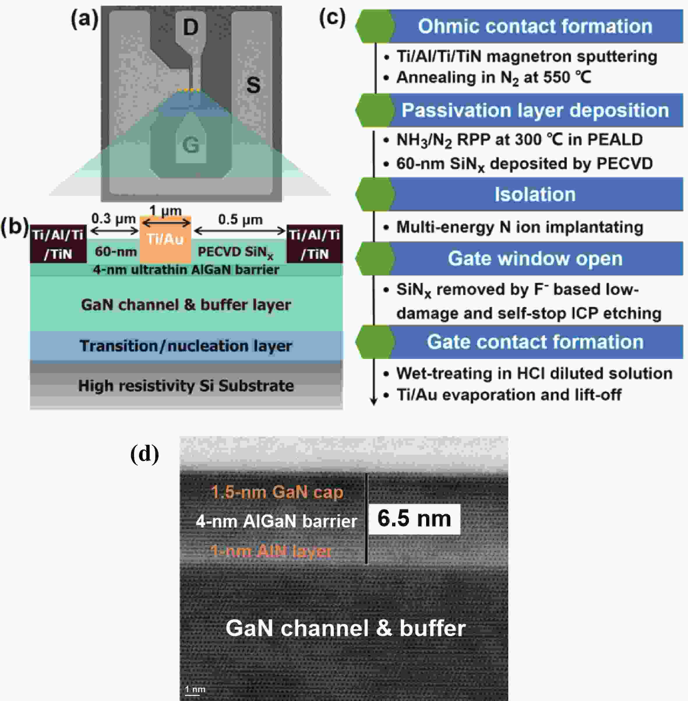
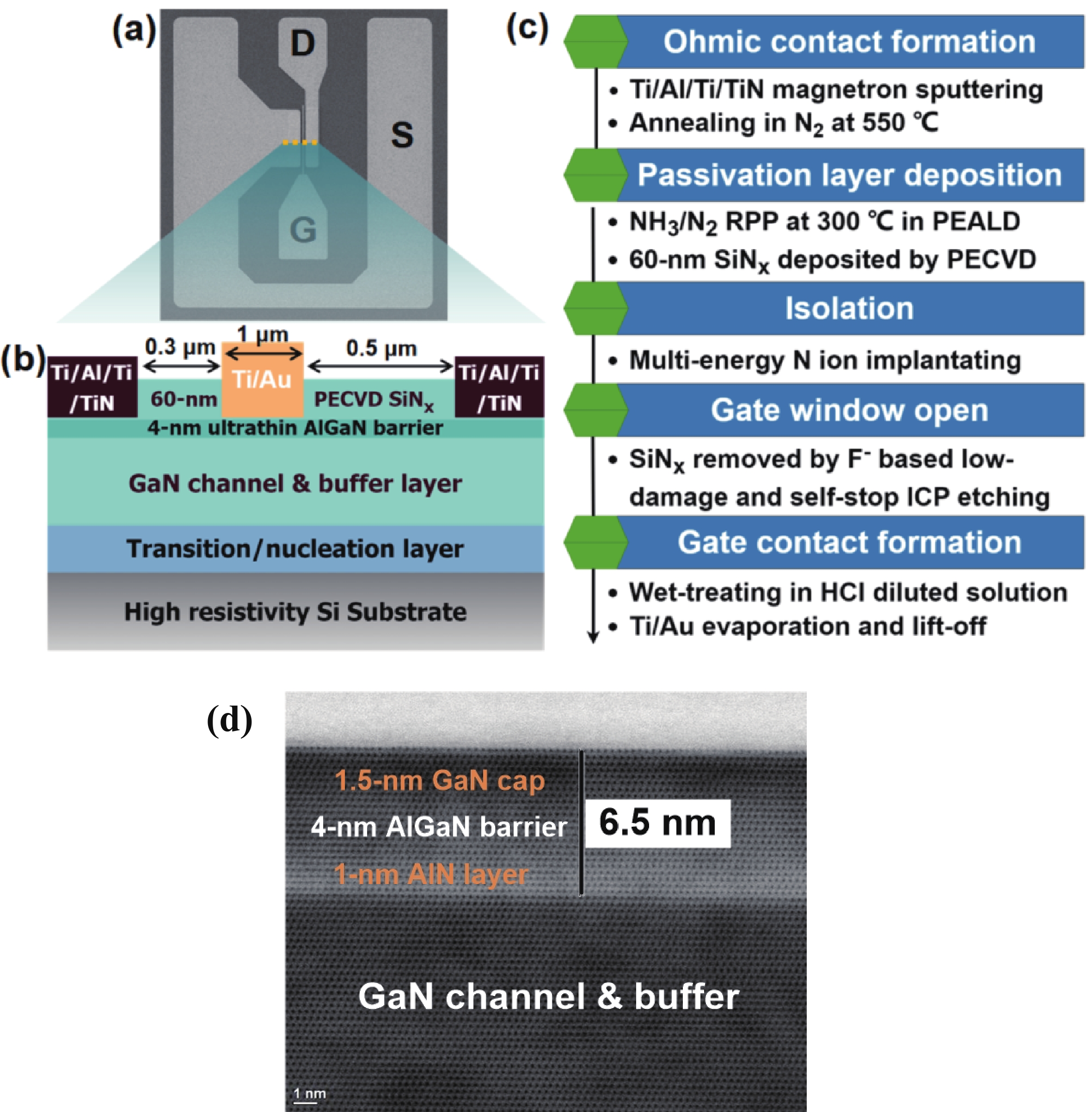
Fig. 1.  (Color online) (a) Scanning electron microscope (SEM) image, (b) cross-sectional schematic, and (c) process flow diagram depicting the fabricated E-mode 1-μm gate UTB-AlGaN/GaN HEMTs on a silicon substrate in this study. The device characteristics LG/WG/LGS/LGD are 1/75/0.3/0.5 μm. (d) A cross-sectional transmission electron microscopy (TEM) image illustrates the UTB-AlGaN/GaN heterostructure. Although there are no observable sharp boundaries among the three layers, the thickness of the different layers is marked according to our design parameters.

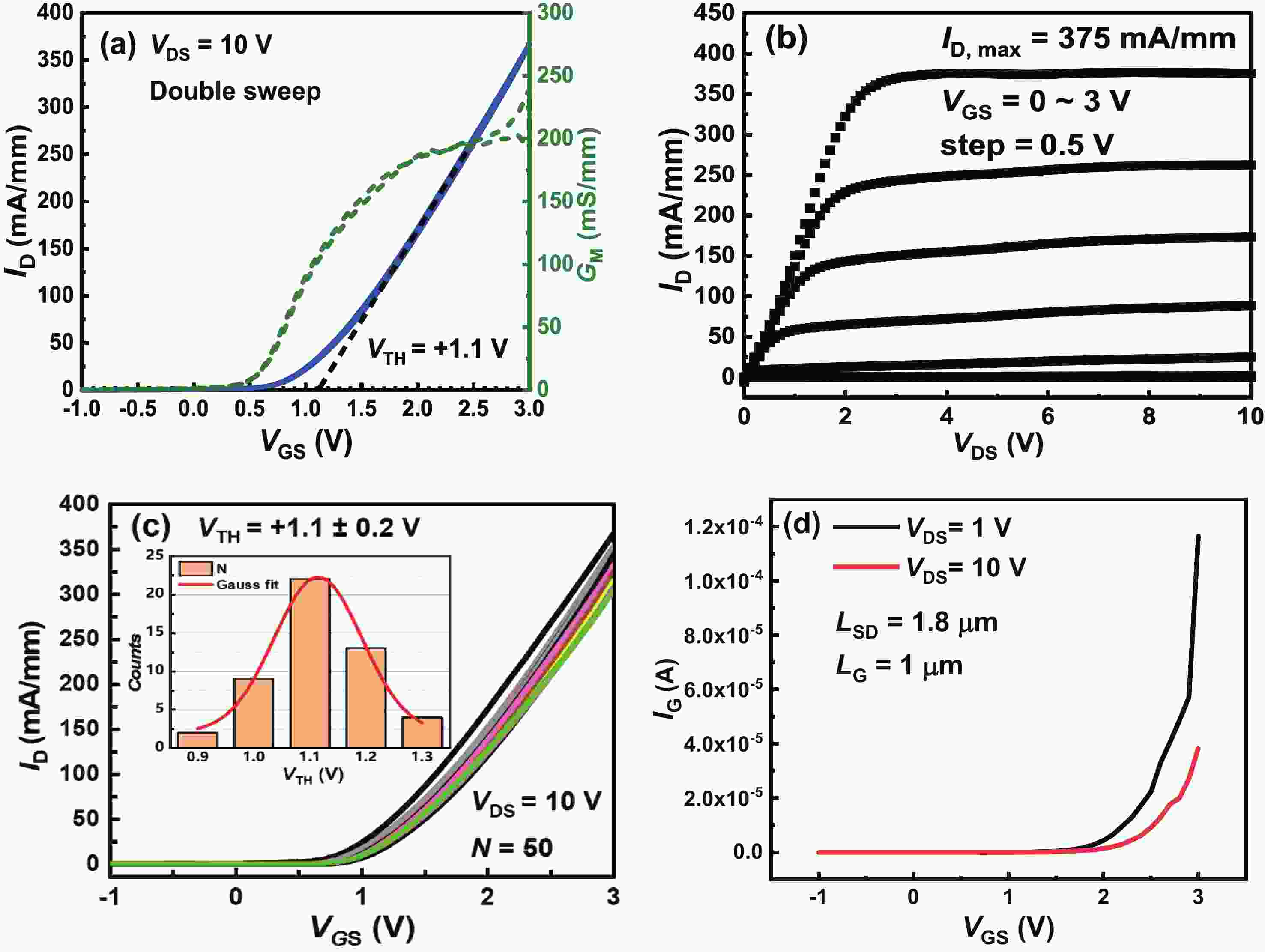
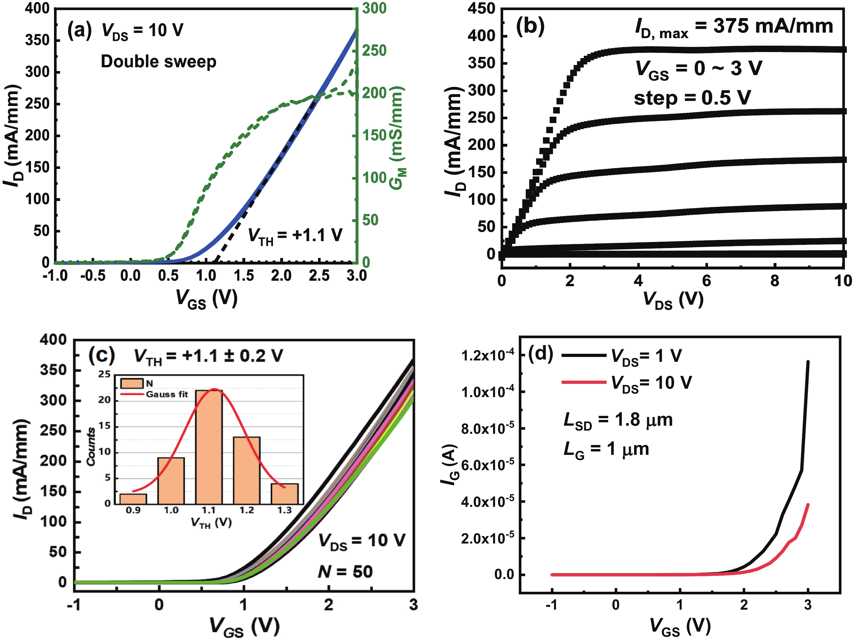
Fig. 2.  (Color online) The DC IV features of the E-mode UTB-AlGaN/GaN HEMTs fabricated on a silicon substrate. The device parameters are specified as follows: LG = 1 μm, WG = 75 μm, and LSD = 1.8 μm. (a) Transfer characteristics are depicted under VDS = 10 V. (b) DC output characteristics are presented. (c) Threshold voltage uniformity is characterized. (d) Gate leakage current is measured under VDS of 1 and 10 V, respectively.

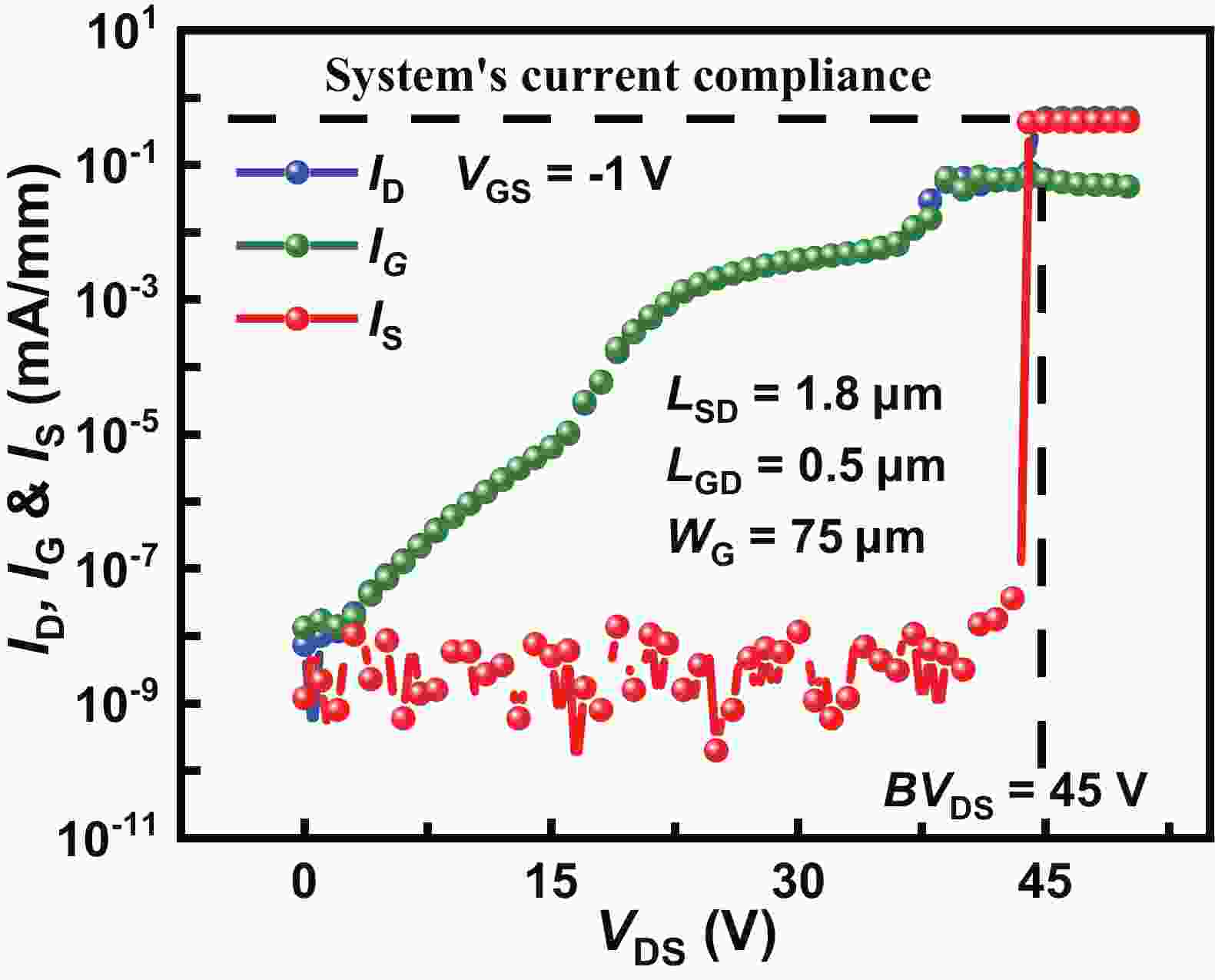
Fig. 3.  (Color online) The off-state breakdown characteristics of the manufactured E-mode UTB-AlGaN/GaN HEMTs on a silicon substrate, with measurements conducted at VGS = −1 V. The device dimensions are as follows: LG = 1 μm, WG = 75 μm, and LSD = 1.8 μm.

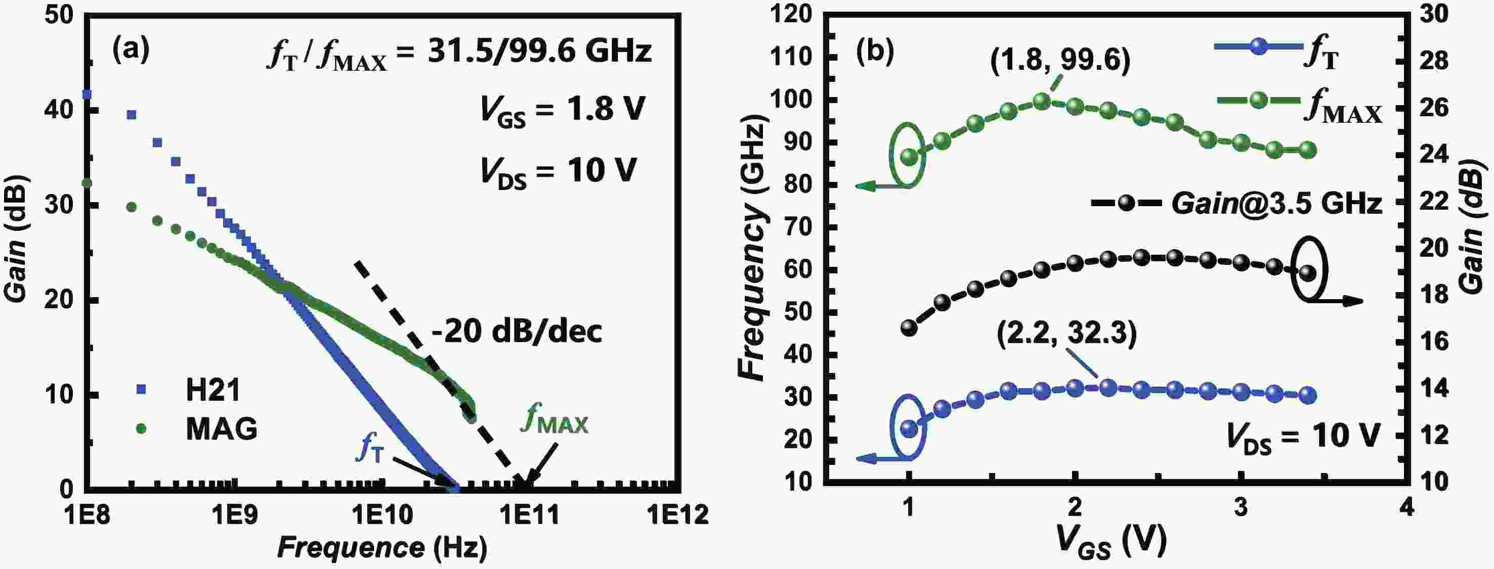
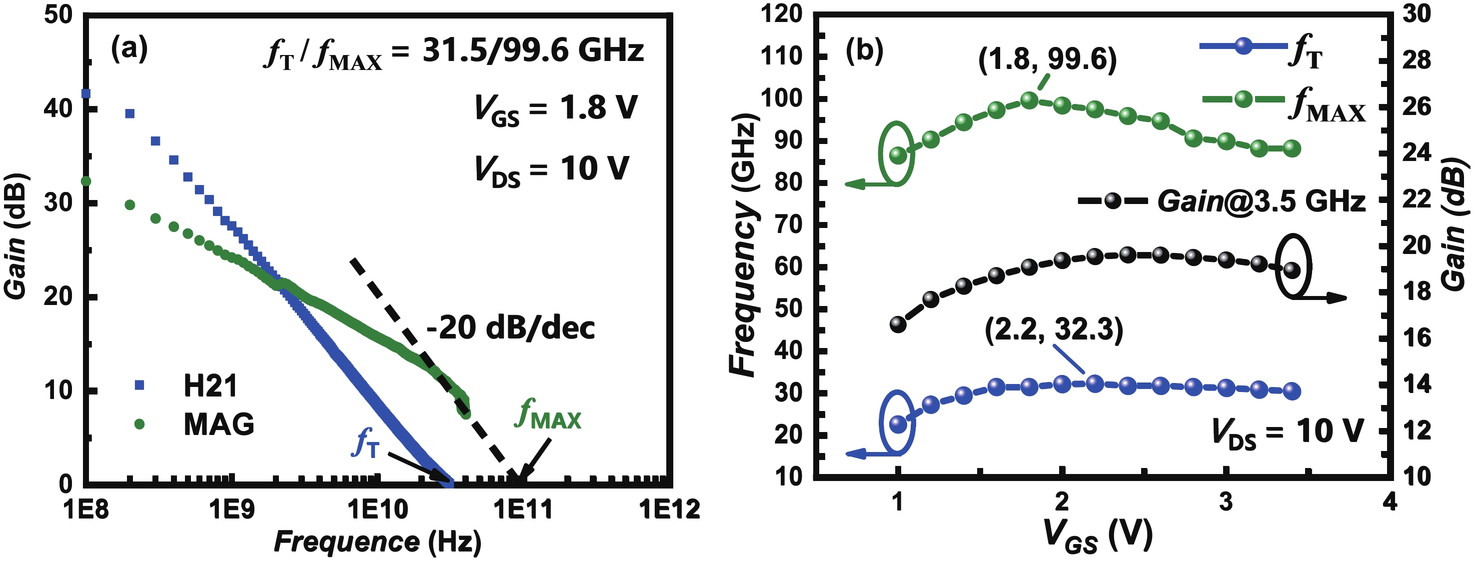
Fig. 4.  (Color online) (a) Radio frequency properties of the produced E-mode UTB-AlGaN/GaN HEMTs under VDS = 10 V and VGS = 1.8 V. The device is characterized with LG/WG/LGS/LGD = 1/75/0.3/0.5 μm. (b) Variation of the fT/fMAX and gain at 3.5 GHz with VGS.

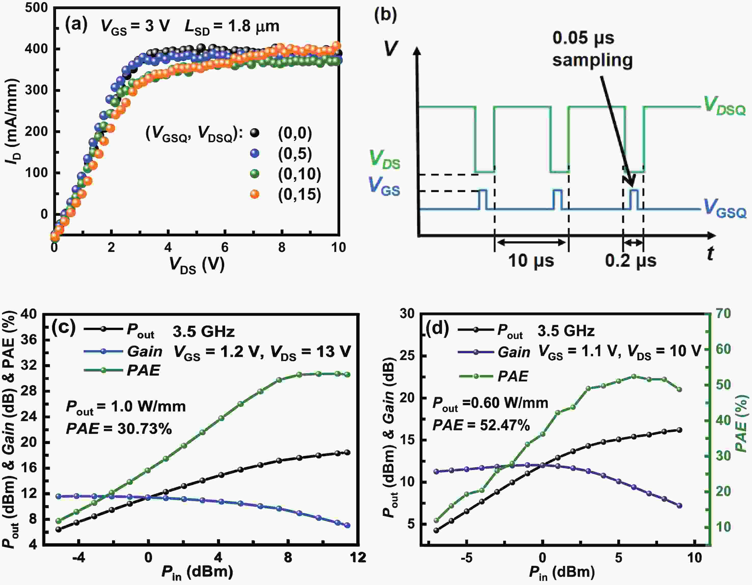
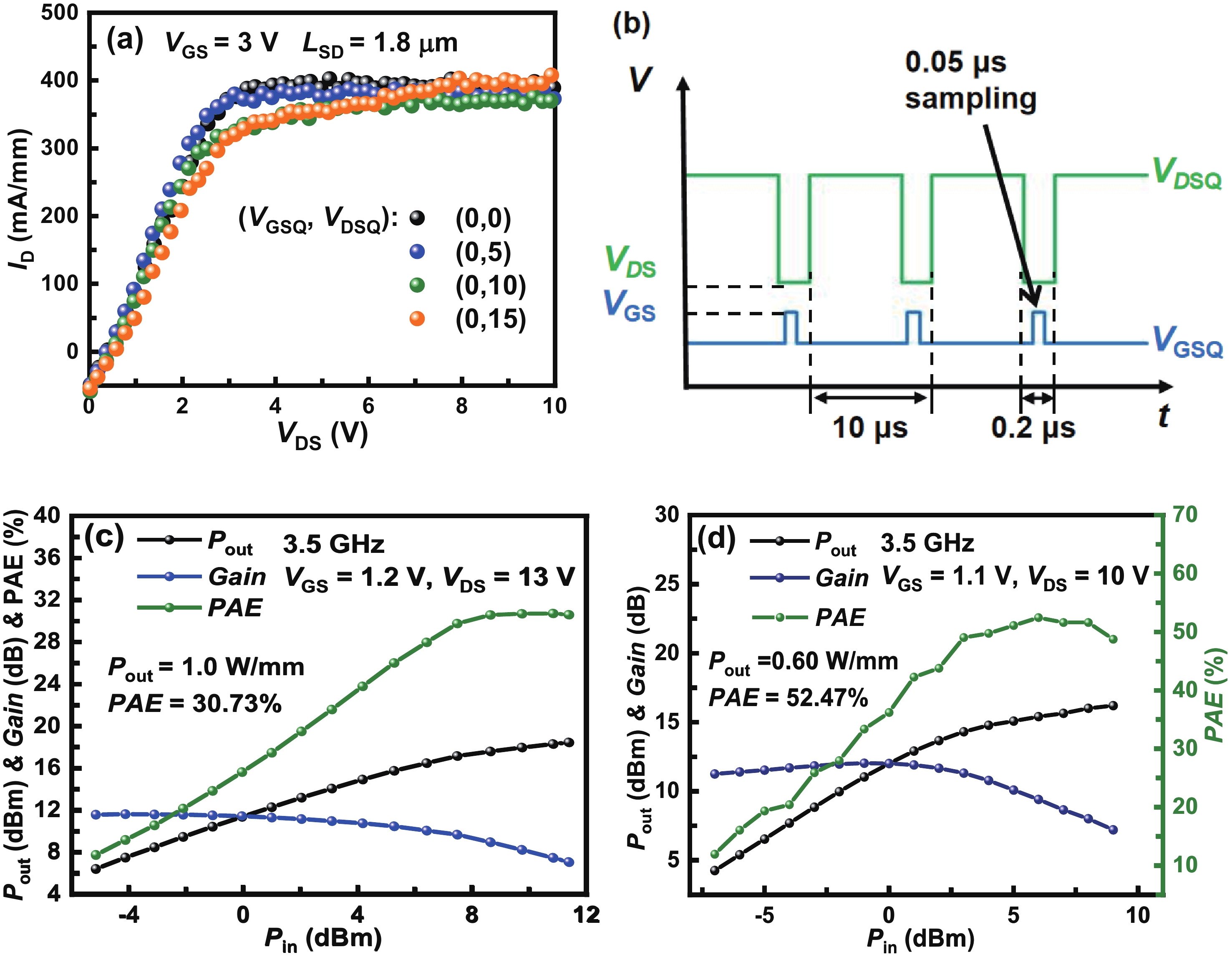
Fig. 5.  (Color online) The pulse current−voltage (IV) characteristics of the manufactured E-mode UTB-AlGaN/GaN HEMTs. (b) A schematic waveform depicts the gate and drain bias variations during the pulsed IV measurement. (c) and (d) Continuous wave power performance is presented at 3.5 GHz for the fabricated E-mode UTB-AlGaN/GaN HEMTs, showcasing different variations in VGS and VDS respectively. The device features dimensions LG/WG/LGS/LGD is 1/75/0.3/0.5 μm.

Table 1.   Summarized RF performances of reported E-mode AlGaN/GaN-on-Si HEMTs.

Reference LG (μm) VTH (V) GM (mS/mm) fT (GHz) fMAX (GHz) POUT (mW/mm) PAE (%)
p-GaN gate
AlGaN/GaN[31]
1 1.5 101.3 6.0 9.8 / /
p-GaN gate
AlGaN/GaN[13]
0.45 0.58 150 22.4 45.3 / /
p-GaN gate
AlGaN/GaN[32]
1 2.7 78 6.1 10.3 1.40 55.40
This work 1 1.1 205 31.3 70.9 1.0 52.47
DownLoad: CSV
[1]
Chen K J, Häberlen O, Lidow A, et al. GaN-on-Si power technology: Devices and applications. IEEE Trans Electron Devices, 2017, 64, 779 doi: 10.1109/TED.2017.2657579
[2]
Zheng Z Y, Zhang L, Song W J, et al. Gallium nitride-based complementary logic integrated circuits. Nat Electron, 2021, 4, 595 doi: 10.1038/s41928-021-00611-y
[3]
Lu H, Hou B, Yang L, et al. High RF performance GaN-on-Si HEMTs with passivation implanted termination. IEEE Electron Device Lett, 2022, 43, 188 doi: 10.1109/LED.2021.3135703
[4]
Zeng Q M, Li X J, Zhou Z, et al. Investigation of undoped AlGaN/GaN microwave power HEMT. J Semicond, 2005, 26, 151
[5]
Chen T S, Zhang B, Ren C J, et al. 14W X-band AlGaN/GaN HEMT power MMICs. J Semicond, 2008, 29, 1027
[6]
Wang D F, Chen X J, Liu X Y. A Ku-band 3.4 W/mm power AlGaN/GaN HEMT on a sapphire substrate. J Semicond, 2010, 31, 024001 doi: 10.1088/1674-4926/31/2/024001
[7]
Hu Y S, Wang Y G, Wang W, et al. 11.2 W/mm power density AlGaN/GaN high electron-mobility transistors on a GaN substrate. J Semicond, 2024, 45, 012501 doi: 10.1088/1674-4926/45/1/012501
[8]
Wang Q, Chen C X, Li W, et al. Fabrication and characterization of AlGaN/GaN HEMTs with high power gain and efficiency at 8 GHz. J Semicond, 2021, 42, 122802 doi: 10.1088/1674-4926/42/12/122802
[9]
Cai Y, Zhou Y G, Chen K J, et al. High-performance enhancement-mode AlGaN/GaN HEMTs using fluoride-based plasma treatment. IEEE Electron Device Lett, 2005, 26, 435 doi: 10.1109/LED.2005.851122
[10]
Wang C, Zhang J F, Quan S, et al. An enhancement-mode AlGaN/GaN HEMT with recessed-gate. J Semicond, 2008, 29, 1692
[11]
Feng Z H, Xie S Y, Zhou R, et al. A high-performance enhancement-mode AlGaN/GaN HEMT. J Semicond, 2010, 31, 084001 doi: 10.1088/1674-4926/31/8/084001
[12]
Liu S Y, Zhu J J, Guo J S, et al. Improved breakdown voltage and low damage E-mode operation of AlON/AlN/GaN HEMTs using plasma oxidation treatment. IEEE Electron Device Lett, 2022, 43, 1621 doi: 10.1109/LED.2022.3203164
[13]
Cheng Y, Ng Y H, Zheng Z Y, et al. RF enhancement-mode p-GaN gate HEMT on 200 mm-Si substrates. IEEE Electron Device Lett, 2023, 44, 29 doi: 10.1109/LED.2022.3220693
[14]
Huang Y L, Zhang L, Cheng Z, et al. AlGaN/GaN high electron mobility transistors with selective area grown p-GaN gates. J Semicond, 2016, 37, 114002 doi: 10.1088/1674-4926/37/11/114002
[15]
Huang S, Liu X Y, Zhang J H, et al. High RF performance enhancement-mode Al2O3/AlGaN/GaN MIS-HEMTs fabricated with high-temperature gate-recess technique. IEEE Electron Device Lett, 2015, 36, 754 doi: 10.1109/LED.2015.2445353
[16]
Hua M Y, Zhang Z F, Wei J, et al. Integration of LPCVD-SiNx gate dielectric with recessed-gate E-mode GaN MIS-FETs: Toward high performance, high stability and long TDDB lifetime. 2016 IEEE International Electron Devices Meeting (IEDM), 2016, 10.4. 1 doi: 10.1109/IEDM.2016.7838388.
[17]
Wang C, Chen Y C, Hsu H T, et al. Adoption of the wet surface treatment technique for the improvement of device performance of enhancement-mode AlGaN/GaN MOSHEMTs for millimeter-wave applications. Materials, 2021, 14, 6558 doi: 10.3390/ma14216558
[18]
Saito W, Takada Y, Kuraguchi M, et al. Recessed-gate structure approach toward normally off high-Voltage AlGaN/GaN HEMT for power electronics applications. IEEE Trans Electron Devices, 2006, 53, 356 doi: 10.1109/TED.2005.862708
[19]
Kanamura M, Ohki T, Kikkawa T, et al. Enhancement-mode GaN MIS-HEMTs with n-GaN/i-AlN/n-GaN triple cap layer and high- $k$ gate dielectrics. IEEE Electron Device Lett, 2010, 31, 189 doi: 10.1109/LED.2009.2039026
[20]
Wang Z L, Zhou J J, Kong Y C, et al. Thin-barrier enhancement-mode AlGaN/GaN MIS-HEMT using ALD Al2O3 as gate insulator. J Semicond, 2015, 36, 094004 doi: 10.1088/1674-4926/36/9/094004
[21]
Huang S, Wang X H, Liu X Y, et al. An ultrathin-barrier AlGaN/GaN heterostructure: A recess-free technology for the fabrication and integration of GaN-based power devices and power-driven circuits. Semicond Sci Technol, 2021, 36, 044002 doi: 10.1088/1361-6641/abd2fe
[22]
Han P C, Yan Z Z, Wu C H, et al. Recess-free normally-off GaN MIS-HEMT fabricated on ultra-thin-barrier AlGaN/GaN heterostructure. 2019 31st International Symposium on Power Semiconductor Devices and ICs (ISPSD), 2019, 427 doi: 10.1109/ISPSD.2019.8757675
[23]
Wu S, Mi M H, Zhang M, et al. A high RF-performance AlGaN/GaN HEMT with ultrathin barrier and stressor in situ SiN. IEEE Trans Electron Devices, 2021, 68, 5553 doi: 10.1109/TED.2021.3111140
[24]
Jessen G H, Fitch R C, Gillespie J K, et al. Short-channel effect limitations on high-frequency operation of AlGaN/GaN HEMTs for T-gate devices. IEEE Trans Electron Devices, 2007, 54, 2589 doi: 10.1109/TED.2007.904476
[25]
Zhou Y W, Mi M H, Gong C, et al. High-efficiency millimeter-wave enhancement-mode ultrathin-barrier AlGaN/GaN fin-HEMT for low-voltage terminal applications. IEEE Trans Electron Devices, 2024, 71, 1383 doi: 10.1109/TED.2023.3276338
[26]
Deng K X, Huang S, Wang X H, et al. Insight into the suppression mechanism of bulk traps in Al2O3 gate dielectric and its effect on threshold voltage instability in Al2O3/AlGaN/GaN metal-oxide-semiconductor high electron mobility transistors. Appl Surf Sci, 2023, 638, 158000 doi: 10.1016/j.apsusc.2023.158000
[27]
Luan T T, Huang S, Yao Y X, et al. 700 V/2.5 A normally-off ultrathin-barrier AlGaN(<6 nm)/GaN MIS-HEMTs with improved gate overdrive window and PBTI. 2023 35th International Symposium on Power Semiconductor Devices and ICs (ISPSD), 2023, 103 doi: 10.1109/ISPSD57135.2023.10147548
[28]
Huang S, Wang X H, Jiang Q M, et al. Ultrathin-barrier AlGaN/GaN heterostructure: An AlGaN-recess-free technology for fabrication of lateral GaN-based power devices. 2022 6th IEEE Electron Devices Technology & Manufacturing Conference (EDTM), 2022, 393 doi: 10.1109/EDTM53872.2022.9797960
[29]
Luan T T, Jiang Q M, Huang S, et al. Investigation of trapping/de-trapping dynamics of surface states in AlGaN/GaN high-electron mobility transistors based on dual-gate structures. Microelectron Eng, 2023, 269, 111916 doi: 10.1016/j.mee.2022.111916
[30]
Ji Y, Huang S, Jiang Q M, et al. Optimization of ohmic contact to ultrathin-barrier AlGaN/GaN heterostructure via an ‘ohmic-before-passivation’ process. Electronics, 2023, 12, 1767 doi: 10.3390/electronics12081767
[31]
Yu C J, Hsu C W, Wu M C, et al. Improved DC and RF performance of novel MIS p-GaN-gated HEMTs by gate-all-around structure. IEEE Electron Device Lett, 2020, 41, 673 doi: 10.1109/LED.2020.2980584
[32]
Zhou J M, Guo H W, Du H T, et al. RF p-GaN HEMT with 0.9-dB noise figure and 12.8-dB associated gain for LNA applications. IEEE Electron Device Lett, 2023, 44, 1412 doi: 10.1109/LED.2023.3294696
  • Search

    Advanced Search >>

    GET CITATION

    shu

    Export: BibTex EndNote

    Article Metrics

    Article views: 146 Times PDF downloads: 31 Times Cited by: 0 Times

    History

    Received: 07 December 2023 Revised: 01 March 2024 Online: Accepted Manuscript: 14 March 2024Uncorrected proof: 14 March 2024

    Catalog

      Email This Article

      User name:
      Email:*请输入正确邮箱
      Code:*验证码错误
      Tiantian Luan, Sen Huang, Guanjun Jing, Jie Fan, Haibo Yin, Xinguo Gao, Sheng Zhang, Ke Wei, Yankui Li, Qimeng Jiang, Xinhua Wang, Bin Hou, Ling Yang, Xiaohua Ma, Xinyu Liu. Recess-free enhancement-mode AlGaN/GaN RF HEMTs on Si substrate[J]. Journal of Semiconductors, 2024, 45(6): 062301. doi: 10.1088/1674-4926/23120006 T T Luan, S Huang, G J Jing, J Fan, H B Yin, X G Gao, S Zhang, K Wei, Y K Li, Q M Jiang, X H Wang, B Hou, L Yang, X H Ma, and X Y Liu, Recess-free enhancement-mode AlGaN/GaN RF HEMTs on Si substrate[J]. J. Semicond., 2024, 45(6), 062301 doi: 10.1088/1674-4926/23120006Export: BibTex EndNote
      Citation:
      Tiantian Luan, Sen Huang, Guanjun Jing, Jie Fan, Haibo Yin, Xinguo Gao, Sheng Zhang, Ke Wei, Yankui Li, Qimeng Jiang, Xinhua Wang, Bin Hou, Ling Yang, Xiaohua Ma, Xinyu Liu. Recess-free enhancement-mode AlGaN/GaN RF HEMTs on Si substrate[J]. Journal of Semiconductors, 2024, 45(6): 062301. doi: 10.1088/1674-4926/23120006

      T T Luan, S Huang, G J Jing, J Fan, H B Yin, X G Gao, S Zhang, K Wei, Y K Li, Q M Jiang, X H Wang, B Hou, L Yang, X H Ma, and X Y Liu, Recess-free enhancement-mode AlGaN/GaN RF HEMTs on Si substrate[J]. J. Semicond., 2024, 45(6), 062301 doi: 10.1088/1674-4926/23120006
      Export: BibTex EndNote

      Recess-free enhancement-mode AlGaN/GaN RF HEMTs on Si substrate

      doi: 10.1088/1674-4926/23120006
      More Information
      • Author Bio:

        Tiantian Luan Tiantian Luan received her BS degree in College of Electronic Science and Engineering from Jilin University, Jilin, China, in 2019. She is pursuing a PhD in microelectronics and solid-state electronics with the Institute of Microelectronics, Chinese Academy of Sciences

        Sen Huang Sen Huang received his PhD degree from Peking University, Beijing, China, in 2009. He is currently a professor at the Institute of Microelectronics, Chinese Academy of Sciences, Beijing. His current research interests include advanced design, fabrication, and characterization technologies for Ⅲ–Ⅴ power semiconductors or devices

      • Corresponding author: huangsen@ime.ac.cn
      • Received Date: 2023-12-07
      • Revised Date: 2024-03-01
      • Available Online: 2024-03-14

      Catalog

        /

        DownLoad:  Full-Size Img  PowerPoint
        Return
        Return