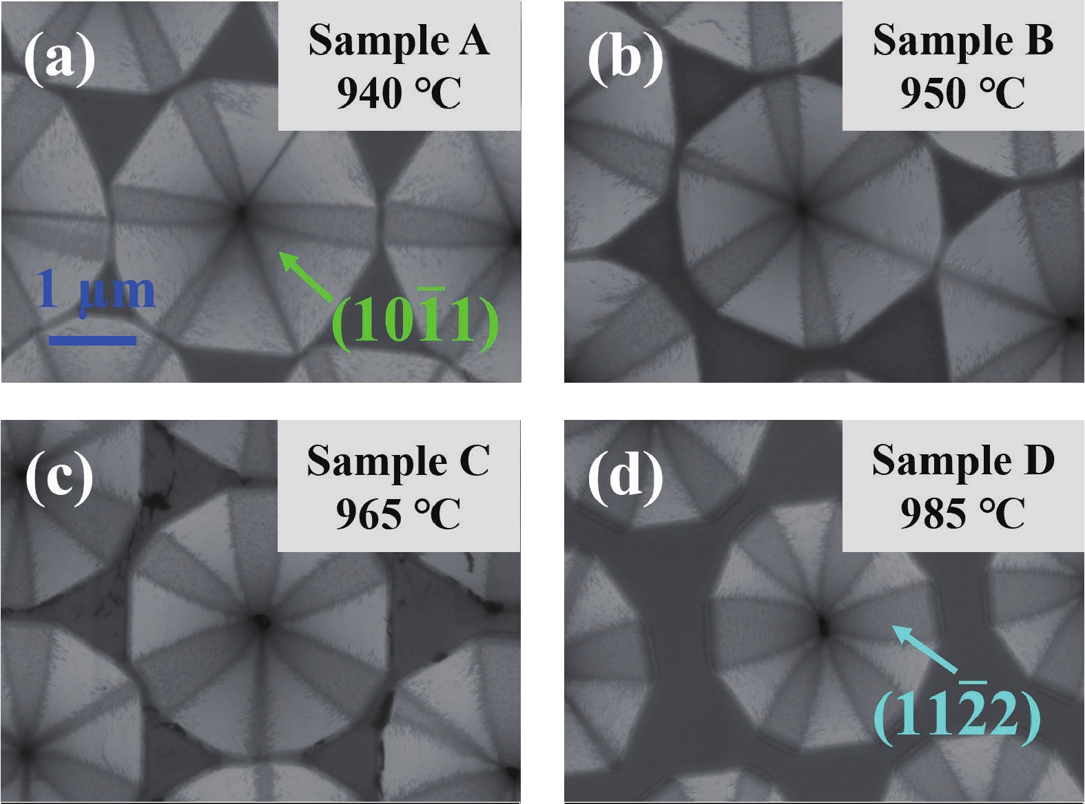
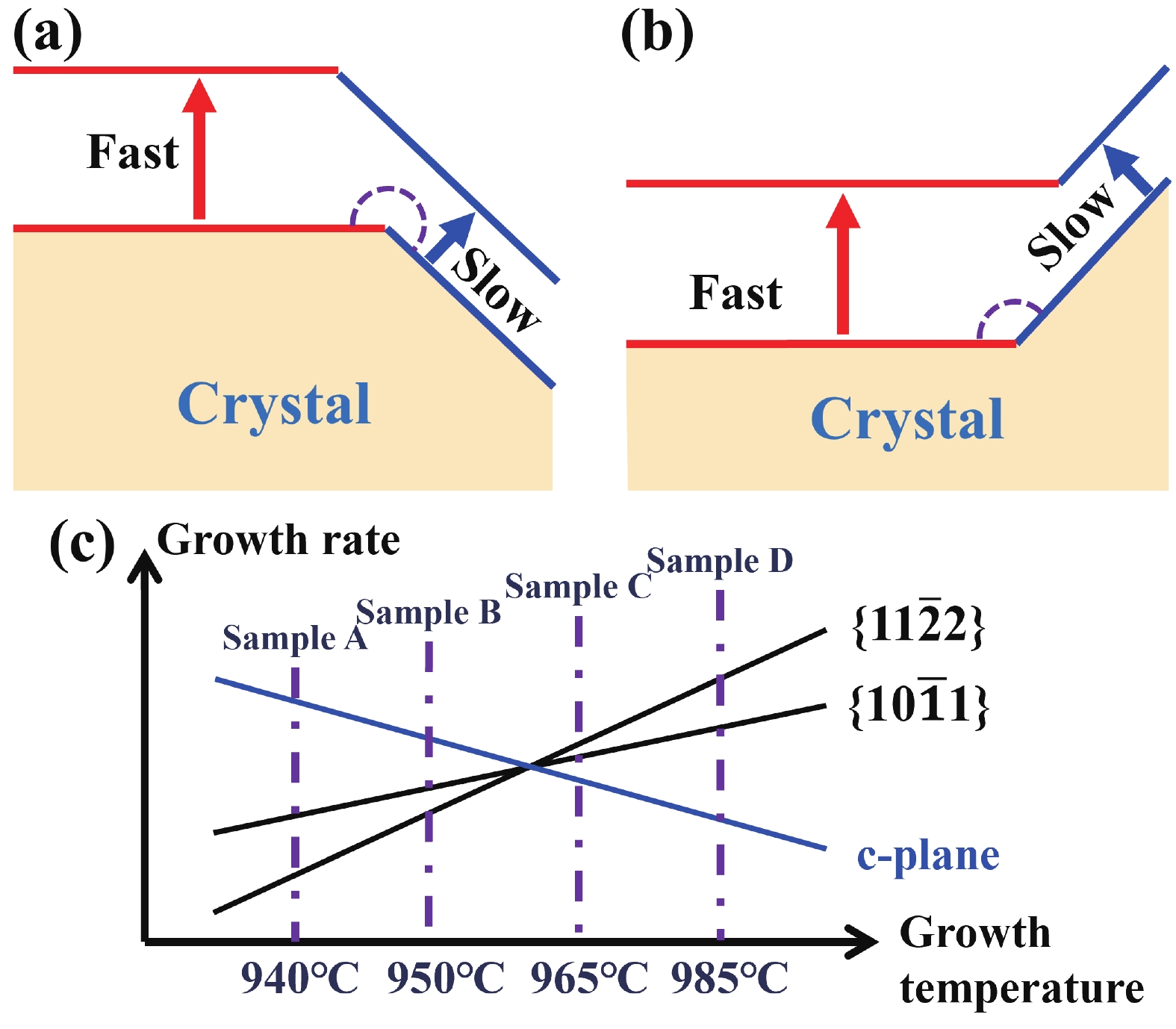
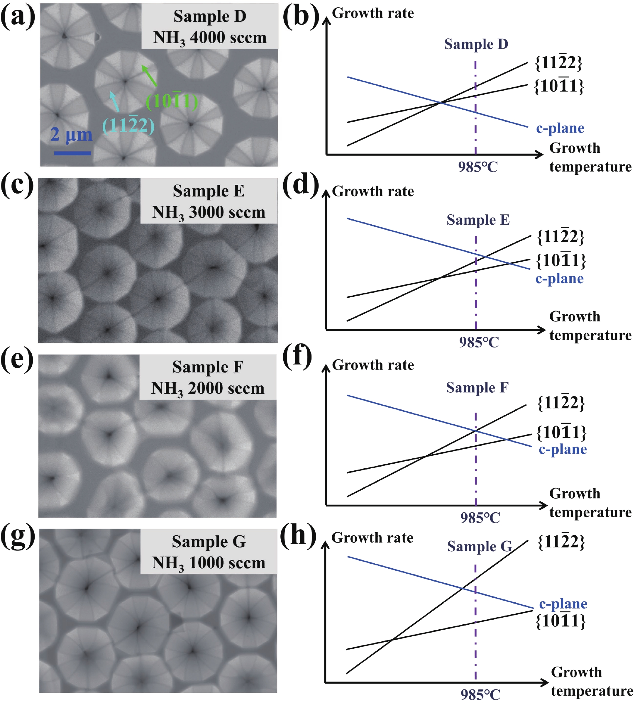
J. Semicond. >  In Press >  doi: 10.1088/1674-4926/24010013

ARTICLES

Control of GaN inverted pyramids growth on c-plane patterned sapphire substrates

Luming Yu1, Xun Wang1, Zhibiao Hao1, 2, Yi Luo1, 2, Changzheng Sun1, 2, Bing Xiong1, 2, Yanjun Han1, 2, Jian Wang1, 2, Hongtao Li1, 2, Lin Gan1, 2 and Lai Wang1, 2,

+ Author Affiliations

 Corresponding author: Lai Wang, wanglai@tsinghua.edu.cn

PDF

Turn off MathJax

Abstract: Growth of gallium nitride (GaN) inverted pyramids on c-plane sapphire substrates is benefit for fabricating novel devices as it forms the semipolar facets. In this work, GaN inverted pyramids are directly grown on c-plane patterned sapphire substrates (PSS) by metal organic vapor phase epitaxy (MOVPE). The influences of growth conditions on the surface morphology are experimentally studied and explained by Wulff constructions. The competition of growth rate among {0001}, {$ 10\bar{\text{1}}1 $}, and {$11 \bar{\text{2}}2 $} facets results in the various surface morphologies of GaN. A higher growth temperature of 985 °C and a lower Ⅴ/Ⅲ ratio of 25 can expand the area of {$ 11\bar{\text{2}}2 $} facets in GaN inverted pyramids. On the other hand, GaN inverted pyramids with almost pure {$10 \bar{\text{1}}1 $} facets are obtained by using a lower growth temperature of 930 °C, a higher Ⅴ/Ⅲ ratio of 100, and PSS with pattern arrangement perpendicular to the substrate primary flat.

Key words: inverted pyramidsGaNMOVPEcrystal growth competition model


[1]
Cai X L, Du C L, Sun Z X, et al. Recent progress of physical failure analysis of GaN HEMTs. J Semicond, 2021, 42, 051801 doi: 10.1088/1674-4926/42/5/051801
[2]
Meneghini M, De Santi C, Abid I, et al. GaN-based power devices: Physics, reliability, and perspectives. J Appl Phys, 2021, 130, 181101 doi: 10.1063/5.0061354
[3]
Li Y Q, Wang X W, Zhang N, et al. Improving the incorporation of indium component for InGaN-based green LED through inserting photonic crystalline in the GaN layer. J Semicond, 2022, 43, 072801 doi: 10.1088/1674-4926/43/7/072801
[4]
Liang F, Yang J, Zhao D G, et al. Room-temperature continuous-wave operation of GaN-based blue-violet laser diodes with a lifetime longer than 1000 H. J Semicond, 2019, 40, 022801 doi: 10.1088/1674-4926/40/2/022801
[5]
Liang F, Zhao D G, Liu Z S, et al. GaN-based blue laser diode with 6.0 W of output power under continuous-wave operation at room temperature. J Semicond, 2021, 42, 112801 doi: 10.1088/1674-4926/42/11/112801
[6]
Nakamura S. The roles of structural imperfections in InGaN-based blue light-emitting diodes and laser diodes. Science, 1998, 281, 955 doi: 10.1126/science.281.5379.956
[7]
Yang J, Zhao D G, Liu Z S, et al. A 357.9 nm GaN/AlGaN multiple quantum well ultraviolet laser diode. J Semicond, 2022, 43, 010501 doi: 10.1088/1674-4926/43/1/010501
[8]
Zhao D G. III-nitride based ultraviolet laser diodes. J Semicond, 2019, 40, 120402 doi: 10.1088/1674-4926/40/12/120402
[9]
Feezell D F, Schmidt M C, DenBaars S P, et al. Development of nonpolar and semipolar InGaN/GaN visible light-emitting diodes. MRS Bull, 2009, 34, 318 doi: 10.1557/mrs2009.93
[10]
Speck J S, Chichibu S F. Nonpolar and semipolar group III nitride-based materials. MRS Bull, 2009, 34, 304 doi: 10.1557/mrs2009.91
[11]
Cho J, Schubert E F, Kim J K. Efficiency droop in light-emitting diodes: Challenges and countermeasures. Laser Photonics Rev, 2013, 7, 408 doi: 10.1002/lpor.201200025
[12]
Xu C, Zheng C D, Wu X M, et al. Effects of V-pits covering layer position on the optoelectronic performance of InGaN green LEDs. J Semicond, 2019, 40, 052801 doi: 10.1088/1674-4926/40/5/052801
[13]
Rajabi K, Wang J X, Jin J, et al. Improving modulation bandwidth of c-plane GaN-based light-emitting diodes by an ultra-thin quantum wells design. Opt Express, 2018, 26, 24985 doi: 10.1364/OE.26.024985
[14]
Zhi T, Tao T, Liu X Y, et al. Low-threshold lasing in a plasmonic laser using nanoplate InGaN/GaN. J Semicond, 2021, 42, 122803 doi: 10.1088/1674-4926/42/12/122803
[15]
Peng R S, Xu S R, Fan X M, et al. Application of nano-patterned InGaN fabricated by self-assembled Ni nano-masks in green InGaN/GaN multiple quantum wells. J Semicond, 2023, 44, 042801 doi: 10.1088/1674-4926/44/4/042801
[16]
Wunderer T, Feneberg M, Lipski F, et al. Three-dimensional GaN for semipolar light emitters. Phys Status Solidi B, 2011, 248, 549 doi: 10.1002/pssb.201046352
[17]
Ward B L, Nam O H, Hartman J D, et al. Electron emission characteristics of GaN pyramid arrays grown via organometallic vapor phase epitaxy. J Appl Phys, 1998, 84, 5238 doi: 10.1063/1.368775
[18]
Scholz F, Wunderer T, Neubert B, et al. GaN-based light-emitting diodes on selectively grown semipolar crystal facets. MRS Bull, 2009, 34, 328 doi: 10.1557/mrs2009.95
[19]
Brubaker M D, Duff S M, Harvey T E, et al. Polarity-controlled GaN/AlN nucleation layers for selective-area growth of GaN nanowire arrays on Si(111) substrates by molecular beam epitaxy. Cryst Growth Des, 2016, 16, 596 doi: 10.1021/acs.cgd.5b00910
[20]
Wang L, Wang X, Bertram F, et al. Color-tunable 3D InGaN/GaN multi-quantum-well light-emitting-diode based on microfacet emission and programmable driving power supply. Adv Opt Mater, 2021, 9, 2001400 doi: 10.1002/adom.202001400
[21]
Herring C. Some theorems on the free energies of crystal surfaces. Phys Rev, 1951, 82, 87 doi: 10.1103/PhysRev.82.87
[22]
Hiramatsu K, Nishiyama K, Motogaito A, et al. Recent progress in selective area growth and epitaxial lateral overgrowth of III-nitrides: Effects of reactor pressure in MOVPE growth. Phys Stat Sol (a), 1999, 176, 535 doi: 10.1002/(SICI)1521-396X(199911)176:1<535::AID-PSSA535>3.0.CO;2-I
[23]
Kung P, Sun C J, Saxler A, et al. Crystallography of epitaxial growth of wurtzite-type thin films on sapphire substrates. J Appl Phys, 1994, 75, 4515 doi: 10.1063/1.355943
Fig. 1.  (Color online) (a) Growth flow chart of GaN inverted pyramid surface structures on PSS. Low temperature buffer layer is grown as nucleation layer at 525 °C. High temperature buffer layer is grown at ~1000 °C to level GaN surface. Finally, GaN inverted pyramid structures are grown due to competition between crystal planes. (b) Cross-sectional SEM image of GaN inverted pyramids.

Fig. 2.  (Color online) SEM images of the surface morphology of 3D GaN with inverted pyramids grown under (a) 940 °C, (b) 950 °C, (c) 965 °C, and (d) 985 °C.

Fig. 3.  (Color online) Schematic diagram of crystal growth competition based on Wulff construction. (a) When the angle between crystal planes is greater than 180°. (b) When the angle between crystal planes is less than 180°. (c) Schematic diagram of the relationship between temperature and growth rate of different facets.

Fig. 4.  (Color online) SEM images of samples with different Ⅴ/Ⅲ ratios at the same growth temperature (985 °C) and their corresponding growth competition models. NH3 flowrate: (a, b) 4000 sccm, (c, d) 3000 sccm, (e, f) 2000 sccm, (g, h) 1000 sccm.

Fig. 5.  (Color online) (a, b) SEM images of sample H and its corresponding growth competition models. (c, d) SEM images of sample H based on rotated PSS and its corresponding growth competition models. The inserts show the arrangement of patterns on PSS/rotated PSS.

Table 1.   Growth conditions of samples.

SampleTMGa flow
rate (sccm)
NH3 flow
rate (sccm)
Ⅴ/Ⅲ
ratio
Temperature
(°C)
A404000100940
B404000100950
C404000100965
D404000100985
E40300075985
F40200050985
G40100025985
H404000100930
DownLoad: CSV
[1]
Cai X L, Du C L, Sun Z X, et al. Recent progress of physical failure analysis of GaN HEMTs. J Semicond, 2021, 42, 051801 doi: 10.1088/1674-4926/42/5/051801
[2]
Meneghini M, De Santi C, Abid I, et al. GaN-based power devices: Physics, reliability, and perspectives. J Appl Phys, 2021, 130, 181101 doi: 10.1063/5.0061354
[3]
Li Y Q, Wang X W, Zhang N, et al. Improving the incorporation of indium component for InGaN-based green LED through inserting photonic crystalline in the GaN layer. J Semicond, 2022, 43, 072801 doi: 10.1088/1674-4926/43/7/072801
[4]
Liang F, Yang J, Zhao D G, et al. Room-temperature continuous-wave operation of GaN-based blue-violet laser diodes with a lifetime longer than 1000 H. J Semicond, 2019, 40, 022801 doi: 10.1088/1674-4926/40/2/022801
[5]
Liang F, Zhao D G, Liu Z S, et al. GaN-based blue laser diode with 6.0 W of output power under continuous-wave operation at room temperature. J Semicond, 2021, 42, 112801 doi: 10.1088/1674-4926/42/11/112801
[6]
Nakamura S. The roles of structural imperfections in InGaN-based blue light-emitting diodes and laser diodes. Science, 1998, 281, 955 doi: 10.1126/science.281.5379.956
[7]
Yang J, Zhao D G, Liu Z S, et al. A 357.9 nm GaN/AlGaN multiple quantum well ultraviolet laser diode. J Semicond, 2022, 43, 010501 doi: 10.1088/1674-4926/43/1/010501
[8]
Zhao D G. III-nitride based ultraviolet laser diodes. J Semicond, 2019, 40, 120402 doi: 10.1088/1674-4926/40/12/120402
[9]
Feezell D F, Schmidt M C, DenBaars S P, et al. Development of nonpolar and semipolar InGaN/GaN visible light-emitting diodes. MRS Bull, 2009, 34, 318 doi: 10.1557/mrs2009.93
[10]
Speck J S, Chichibu S F. Nonpolar and semipolar group III nitride-based materials. MRS Bull, 2009, 34, 304 doi: 10.1557/mrs2009.91
[11]
Cho J, Schubert E F, Kim J K. Efficiency droop in light-emitting diodes: Challenges and countermeasures. Laser Photonics Rev, 2013, 7, 408 doi: 10.1002/lpor.201200025
[12]
Xu C, Zheng C D, Wu X M, et al. Effects of V-pits covering layer position on the optoelectronic performance of InGaN green LEDs. J Semicond, 2019, 40, 052801 doi: 10.1088/1674-4926/40/5/052801
[13]
Rajabi K, Wang J X, Jin J, et al. Improving modulation bandwidth of c-plane GaN-based light-emitting diodes by an ultra-thin quantum wells design. Opt Express, 2018, 26, 24985 doi: 10.1364/OE.26.024985
[14]
Zhi T, Tao T, Liu X Y, et al. Low-threshold lasing in a plasmonic laser using nanoplate InGaN/GaN. J Semicond, 2021, 42, 122803 doi: 10.1088/1674-4926/42/12/122803
[15]
Peng R S, Xu S R, Fan X M, et al. Application of nano-patterned InGaN fabricated by self-assembled Ni nano-masks in green InGaN/GaN multiple quantum wells. J Semicond, 2023, 44, 042801 doi: 10.1088/1674-4926/44/4/042801
[16]
Wunderer T, Feneberg M, Lipski F, et al. Three-dimensional GaN for semipolar light emitters. Phys Status Solidi B, 2011, 248, 549 doi: 10.1002/pssb.201046352
[17]
Ward B L, Nam O H, Hartman J D, et al. Electron emission characteristics of GaN pyramid arrays grown via organometallic vapor phase epitaxy. J Appl Phys, 1998, 84, 5238 doi: 10.1063/1.368775
[18]
Scholz F, Wunderer T, Neubert B, et al. GaN-based light-emitting diodes on selectively grown semipolar crystal facets. MRS Bull, 2009, 34, 328 doi: 10.1557/mrs2009.95
[19]
Brubaker M D, Duff S M, Harvey T E, et al. Polarity-controlled GaN/AlN nucleation layers for selective-area growth of GaN nanowire arrays on Si(111) substrates by molecular beam epitaxy. Cryst Growth Des, 2016, 16, 596 doi: 10.1021/acs.cgd.5b00910
[20]
Wang L, Wang X, Bertram F, et al. Color-tunable 3D InGaN/GaN multi-quantum-well light-emitting-diode based on microfacet emission and programmable driving power supply. Adv Opt Mater, 2021, 9, 2001400 doi: 10.1002/adom.202001400
[21]
Herring C. Some theorems on the free energies of crystal surfaces. Phys Rev, 1951, 82, 87 doi: 10.1103/PhysRev.82.87
[22]
Hiramatsu K, Nishiyama K, Motogaito A, et al. Recent progress in selective area growth and epitaxial lateral overgrowth of III-nitrides: Effects of reactor pressure in MOVPE growth. Phys Stat Sol (a), 1999, 176, 535 doi: 10.1002/(SICI)1521-396X(199911)176:1<535::AID-PSSA535>3.0.CO;2-I
[23]
Kung P, Sun C J, Saxler A, et al. Crystallography of epitaxial growth of wurtzite-type thin films on sapphire substrates. J Appl Phys, 1994, 75, 4515 doi: 10.1063/1.355943
  • Search

    Advanced Search >>

    GET CITATION

    shu

    Export: BibTex EndNote

    Article Metrics

    Article views: 164 Times PDF downloads: 39 Times Cited by: 0 Times

    History

    Received: 09 January 2024 Revised: 22 January 2024 Online: Accepted Manuscript: 01 March 2024Uncorrected proof: 06 March 2024

    Catalog

      Email This Article

      User name:
      Email:*请输入正确邮箱
      Code:*验证码错误
      Luming Yu, Xun Wang, Zhibiao Hao, Yi Luo, Changzheng Sun, Bing Xiong, Yanjun Han, Jian Wang, Hongtao Li, Lin Gan, Lai Wang. Control of GaN inverted pyramids growth on c-plane patterned sapphire substrates[J]. Journal of Semiconductors, 2024, 45(6): 062501. doi: 10.1088/1674-4926/24010013 L M Yu, X Wang, Z B Hao, Y Luo, C Z Sun, B Xiong, Y J Han, J Wang, H T Li, L Gan, and L Wang, Control of GaN inverted pyramids growth on c-plane patterned sapphire substrates[J]. J. Semicond., 2024, 45(6), 062501 doi: 10.1088/1674-4926/24010013Export: BibTex EndNote
      Citation:
      Luming Yu, Xun Wang, Zhibiao Hao, Yi Luo, Changzheng Sun, Bing Xiong, Yanjun Han, Jian Wang, Hongtao Li, Lin Gan, Lai Wang. Control of GaN inverted pyramids growth on c-plane patterned sapphire substrates[J]. Journal of Semiconductors, 2024, 45(6): 062501. doi: 10.1088/1674-4926/24010013

      L M Yu, X Wang, Z B Hao, Y Luo, C Z Sun, B Xiong, Y J Han, J Wang, H T Li, L Gan, and L Wang, Control of GaN inverted pyramids growth on c-plane patterned sapphire substrates[J]. J. Semicond., 2024, 45(6), 062501 doi: 10.1088/1674-4926/24010013
      Export: BibTex EndNote

      Control of GaN inverted pyramids growth on c-plane patterned sapphire substrates

      doi: 10.1088/1674-4926/24010013
      More Information
      • Author Bio:

        Luming Yu Luming Yu got his bachelor’s degree in 2019 from Department of Electronic Engineering of Tsinghua University. Now he is a doctoral student at Tsinghua University under the supervision of Prof. Lai Wang. His research focuses on MOCVD growth, quantum dots and Micro-LEDs for display and communication

        Lai Wang Lai Wang received his bachelor's degree and doctor's degree respectively, both in the Department of Electronic Engineering of Tsinghua University in 2003 and 2008, respectively. His research interests include optoelectronic materials and devices based on wide-gap semiconductors, Micro-LEDs for display and communication, blue and green laser diodes, and in-sensor computing devices. He has published more than 150 SCI papers. In 2011, he won the second prize of National Science and Technology Progress Award. In 2022, he was supported by the National Science Fund for Distinguished Young Scholars

      • Corresponding author: wanglai@tsinghua.edu.cn
      • Received Date: 2024-01-09
      • Revised Date: 2024-01-22
      • Available Online: 2024-03-01

      Catalog

        /

        DownLoad:  Full-Size Img  PowerPoint
        Return
        Return