


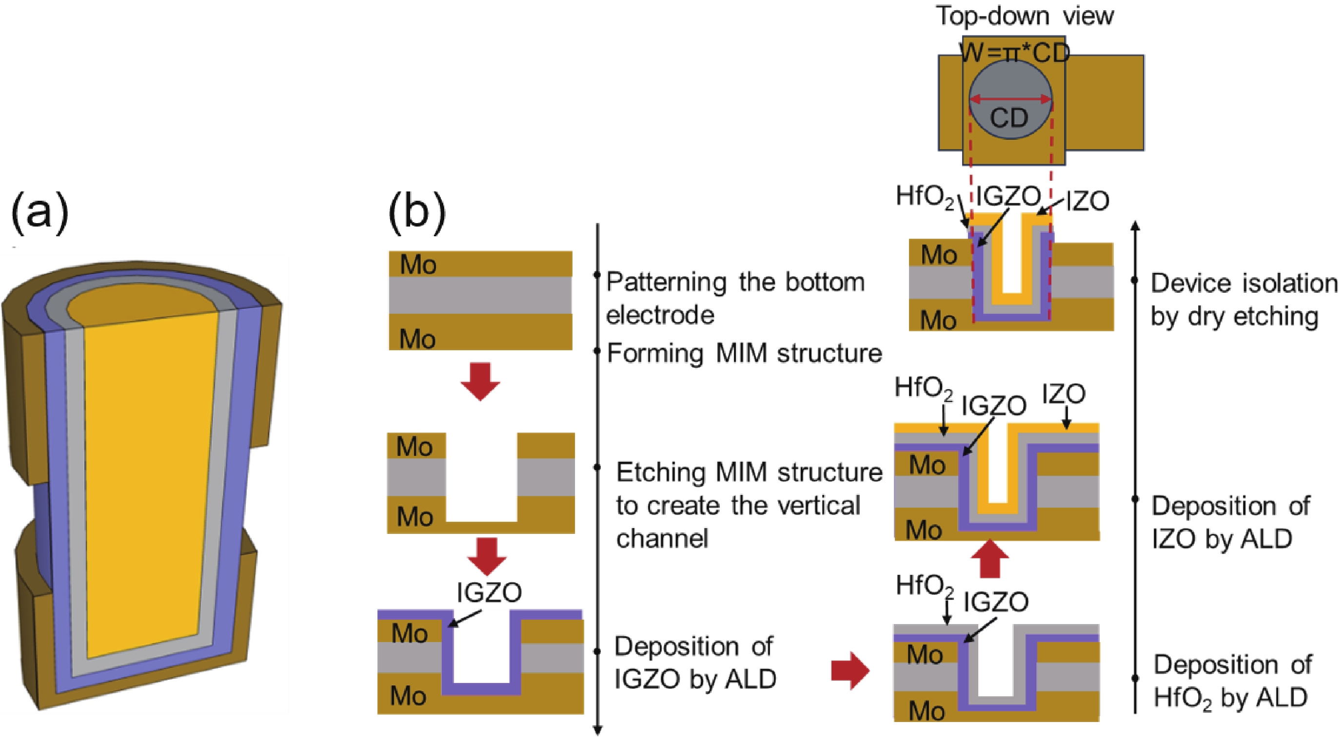
Fig. 1.
(Color online) (a) The structure of IGZO TET with a CAA structure; (b) the process flow of CAA IGZO TFT fabrication.
ARTICLES
Yuting Chen1, §, Xinlv Duan2, §, Xueli Ma1, , Peng Yuan1, Zhengying Jiao1, Yongqing Shen1, Liguo Chai1, Qingjie Luan1, JinJuan Xiang1, , Di Geng2, Guilei Wang1, and Chao Zhao1
Corresponding author: Xueli Ma, Xueli.Ma@bjsamt.org.cn; JinJuan Xiang, Jinjuan.Xiang@bjsamt.org.cn; Guilei Wang, Guilei.Wang@bjsamt.org.cn
Abstract: In–Ga–Zn–O (IGZO) channel based thin-film transistors (TFT), which exhibit high on–off current ratio and relatively high mobility, has been widely researched due to its back end of line (BEOL)-compatible potential for the next generation dynamic random access memory (DRAM) application. In this work, thermal atomic layer deposition (TALD) indium gallium zinc oxide (IGZO) technology was explored. It was found that the atomic composition and the physical properties of the IGZO films can be modulated by changing the sub-cycles number during atomic layer deposition (ALD) process. In addition, thin-film transistors (TFTs) with vertical channel-all-around (CAA) structure were realized to explore the influence of different IGZO films as channel layers on the performance of transistors. Our research demonstrates that TALD is crucial for high density integration technology, and the proposed vertical IGZO CAA-TFT provides a feasible path to break through the technical problems for the continuous scale of electronic equipment.
Key words: In–Ga–Zn–O (IGZO), thermal atomic layer deposition, vertical channel, thin-film transistor
| [1] |
Fortunato E, Barquinha P, Martins R. Oxide semiconductor thin-film transistors: A review of recent advances. Adv Mater, 2012, 24, 2945 doi: 10.1002/adma.201103228
|
| [2] |
Duan X F, Niu C M, Sahi V, et al. High-performance thin-film transistors using semiconductor nanowires and nanoribbons. Nature, 2003, 425, 274 doi: 10.1038/nature01996
|
| [3] |
Myny K. The development of flexible integrated circuits based on thin-film transistors. Nat Electron, 2018, 1, 30 doi: 10.1038/s41928-017-0008-6
|
| [4] |
Lee H, Chang K S, Tak Y J, et al. Electric field-aided selective activation for indium-gallium-zinc-oxide thin film transistors. Sci Rep, 2016, 6, 35044 doi: 10.1038/srep35044
|
| [5] |
Kim J I, Hwan Ji K, Yoon Jung H, et al. Improvement in both mobility and bias stability of ZnSnO transistors by inserting ultra-thin InSnO layer at the gate insulator/channel interface. Appl Phys Lett, 2011, 99, 122102 doi: 10.1063/1.3643054
|
| [6] |
Nomura K, Ohta H, Takagi A, et al. Room-temperature fabrication of transparent flexible thin-film transistors using amorphous oxide semiconductors. Nature, 2004, 432, 488 doi: 10.1038/nature03090
|
| [7] |
Yu M J, Yeh Y H, Cheng C C, et al. Amorphous InGaZnO thin-film transistors compatible with roll-to-roll fabrication at room temperature. IEEE Electron Device Lett, 2012, 33, 47 doi: 10.1109/LED.2011.2170809
|
| [8] |
Nathan A, Lee S, Jeon S, et al. Amorphous oxide semiconductor TFTs for displays and imaging. J Disp Technol, 2014, 10, 917 doi: 10.1109/JDT.2013.2292580
|
| [9] |
Kamiya T, Hosono H. Material characteristics and applications of transparent amorphous oxide semiconductors. NPG Asia Mater, 2010, 2, 15 doi: 10.1038/asiamat.2010.5
|
| [10] |
Mao S J, Wang G L, Zhao C. Amorphous oxide semiconductor for monolithic 3D DRAM: An enabler or passer-by? Natl Sci Rev, 2024, 11, nwad290 doi: 10.1093/nsr/nwad290
|
| [11] |
Liu Y, Zhou H L, Cheng R, et al. Highly flexible electronics from scalable vertical thin film transistors. Nano Lett, 2014, 14, 1413 doi: 10.1021/nl404484s
|
| [12] |
Ho Rha S, Jung J, Soo Jung Y, et al. Vertically integrated submicron amorphous-In2Ga2ZnO7 thin film transistor using a low temperature process. Appl Phys Lett, 2012, 100, 203510 doi: 10.1063/1.4717621
|
| [13] |
Duan X L, Huang K L, Feng J X, et al. Novel vertical channel-all-around (CAA) IGZO FETs for 2T0C DRAM with high density beyond 4F2 by monolithic stacking. 2021 IEEE International Electron Devices Meeting (IEDM). San Francisco, CA, USA. IEEE, 2021, 2196 doi: 10.1109/TED.2022.3154693
|
| [14] |
Sheng J Z, Lee H J, Oh S, et al. Flexible and high-performance amorphous indium zinc oxide thin-film transistor using low-temperature atomic layer deposition. ACS Appl Mater Interfaces, 2016, 8, 33821 doi: 10.1021/acsami.6b11774
|
| [15] |
Illiberi A, Cobb B, Sharma A, et al. Spatial atmospheric atomic layer deposition of InxGayZnzO for thin film transistors. ACS Appl Mater Interfaces, 2015, 7, 3671 doi: 10.1021/am508071y
|
| [16] |
Choi S N, Yoon S M. Implementation of In–Ga–Zn–O thin-film transistors with vertical channel structures designed with atomic-layer deposition and silicon spacer steps. Electron Mater Lett, 2021, 17, 485 doi: 10.1007/s13391-021-00307-7
|
| [17] |
Kim G H, Jeong W H, Kim H J. Electrical characteristics of solution-processed InGaZnO thin film transistors depending on Ga concentration. Phys Status Solidi A, 2010, 207, 1677 doi: 10.1002/pssa.200983742
|
| [18] |
Cho M H, Kim M J, Seul H, et al. Impact of cation compositions on the performance of thin-film transistors with amorphous indium gallium zinc oxide grown through atomic layer deposition. J Inf Disp, 2019, 20, 73 doi: 10.1080/15980316.2018.1540365
|
| [19] |
Nam Y, Kim H O, Cho S H, et al. Effect of hydrogen diffusion in an In–Ga–Zn–O thin film transistor with an aluminum oxide gate insulator on its electrical properties. RSC Adv, 2018, 8, 5622 doi: 10.1039/C7RA12841J
|
| [20] |
Cho M H, Choi C H, Seul H J, et al. Achieving a low-voltage, high-mobility IGZO transistor through an ALD-derived bilayer channel and a hafnia-based gate dielectric stack. ACS Appl Mater Interfaces, 2021, 13, 16628 doi: 10.1021/acsami.0c22677
|
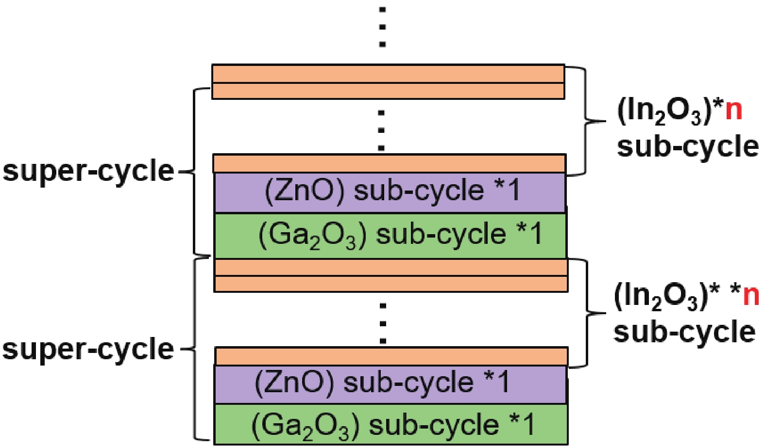
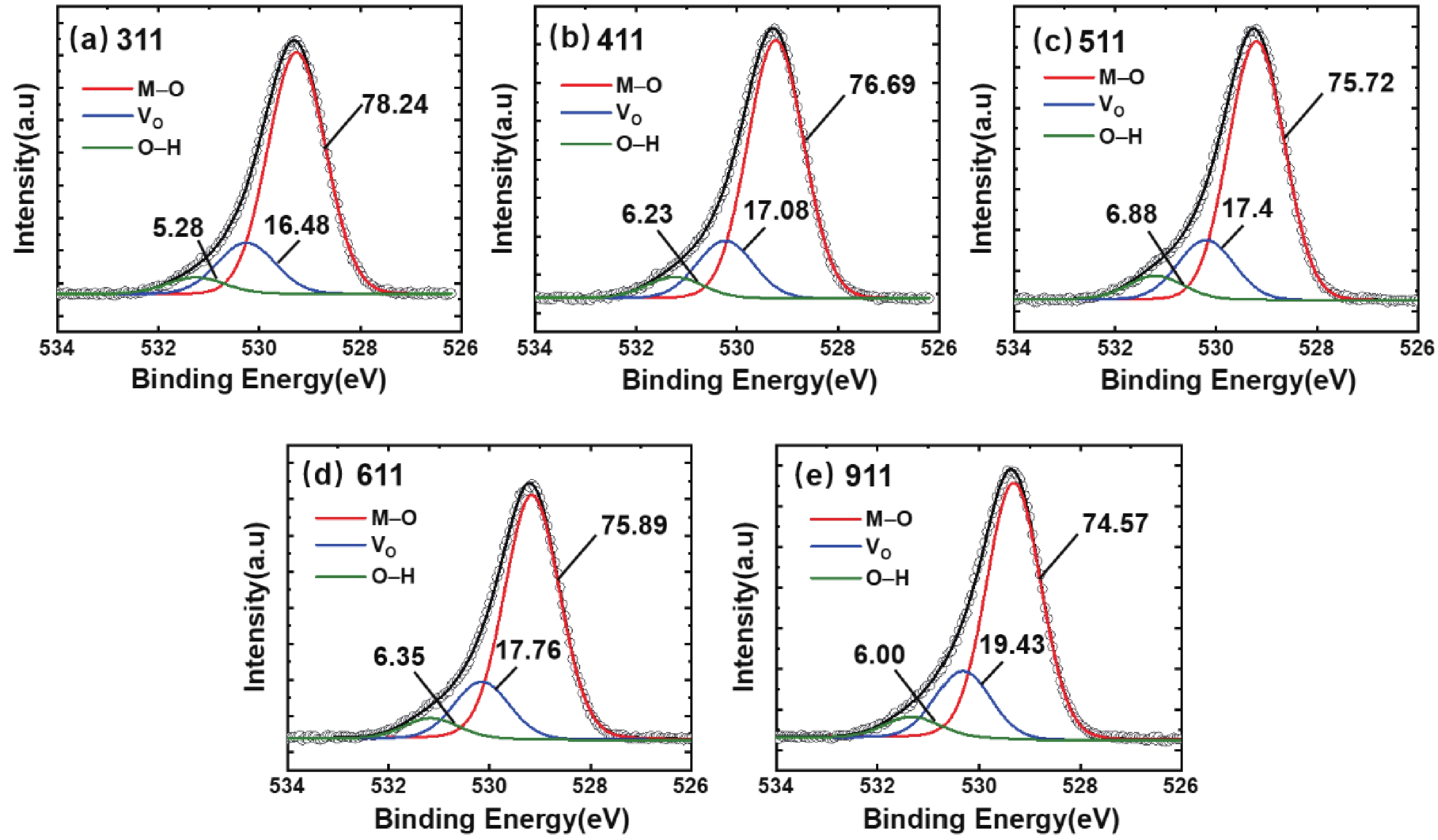
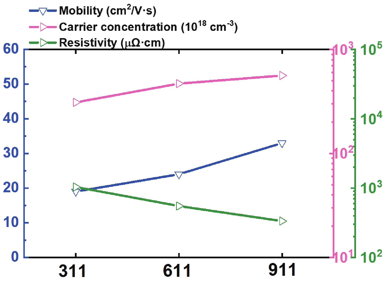
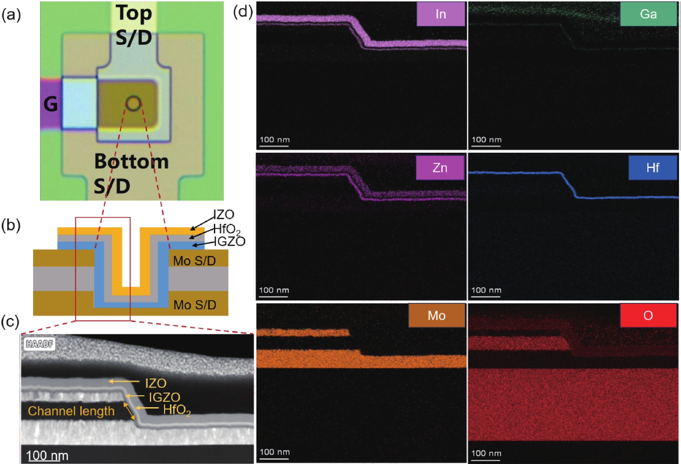
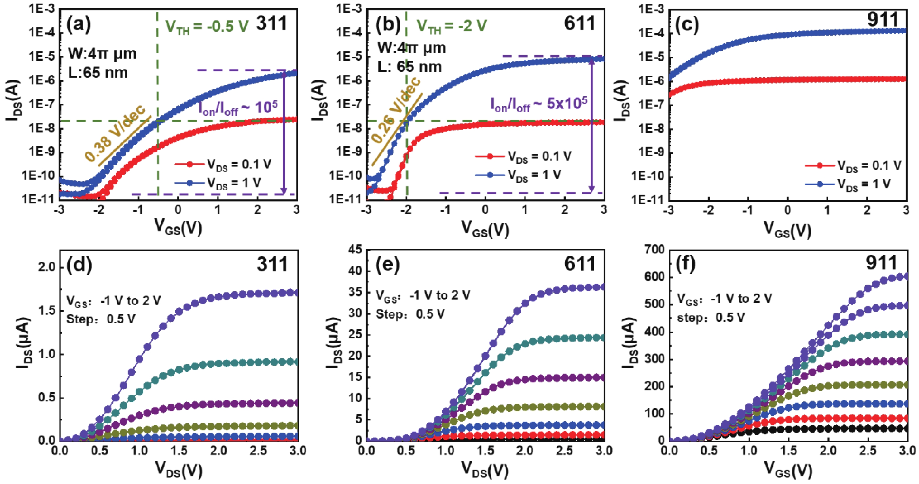
Table 1. Atomic percentage of IGZO thin films with various In2O3 sub-cycles.
| Sample | In (%) | Ga (%) | Zn (%) | O (%) | In/Ga | Zn/Ga |
| 311 | 18.23 | 13.34 | 17.55 | 50.77 | 1.36 | 1.3 |
| 411 | 21.03 | 11.14 | 15.16 | 52.68 | 1.89 | 1.36 |
| 511 | 22.38 | 10.34 | 15.02 | 52.26 | 2.16 | 1.45 |
| 611 | 24.35 | 9.54 | 13.29 | 52.82 | 2.55 | 1.39 |
| 911 | 28.74 | 7.22 | 9.39 | 54.65 | 3.98 | 1.3 |
 DownLoad: CSV
| [1] |
Fortunato E, Barquinha P, Martins R. Oxide semiconductor thin-film transistors: A review of recent advances. Adv Mater, 2012, 24, 2945 doi: 10.1002/adma.201103228
|
| [2] |
Duan X F, Niu C M, Sahi V, et al. High-performance thin-film transistors using semiconductor nanowires and nanoribbons. Nature, 2003, 425, 274 doi: 10.1038/nature01996
|
| [3] |
Myny K. The development of flexible integrated circuits based on thin-film transistors. Nat Electron, 2018, 1, 30 doi: 10.1038/s41928-017-0008-6
|
| [4] |
Lee H, Chang K S, Tak Y J, et al. Electric field-aided selective activation for indium-gallium-zinc-oxide thin film transistors. Sci Rep, 2016, 6, 35044 doi: 10.1038/srep35044
|
| [5] |
Kim J I, Hwan Ji K, Yoon Jung H, et al. Improvement in both mobility and bias stability of ZnSnO transistors by inserting ultra-thin InSnO layer at the gate insulator/channel interface. Appl Phys Lett, 2011, 99, 122102 doi: 10.1063/1.3643054
|
| [6] |
Nomura K, Ohta H, Takagi A, et al. Room-temperature fabrication of transparent flexible thin-film transistors using amorphous oxide semiconductors. Nature, 2004, 432, 488 doi: 10.1038/nature03090
|
| [7] |
Yu M J, Yeh Y H, Cheng C C, et al. Amorphous InGaZnO thin-film transistors compatible with roll-to-roll fabrication at room temperature. IEEE Electron Device Lett, 2012, 33, 47 doi: 10.1109/LED.2011.2170809
|
| [8] |
Nathan A, Lee S, Jeon S, et al. Amorphous oxide semiconductor TFTs for displays and imaging. J Disp Technol, 2014, 10, 917 doi: 10.1109/JDT.2013.2292580
|
| [9] |
Kamiya T, Hosono H. Material characteristics and applications of transparent amorphous oxide semiconductors. NPG Asia Mater, 2010, 2, 15 doi: 10.1038/asiamat.2010.5
|
| [10] |
Mao S J, Wang G L, Zhao C. Amorphous oxide semiconductor for monolithic 3D DRAM: An enabler or passer-by? Natl Sci Rev, 2024, 11, nwad290 doi: 10.1093/nsr/nwad290
|
| [11] |
Liu Y, Zhou H L, Cheng R, et al. Highly flexible electronics from scalable vertical thin film transistors. Nano Lett, 2014, 14, 1413 doi: 10.1021/nl404484s
|
| [12] |
Ho Rha S, Jung J, Soo Jung Y, et al. Vertically integrated submicron amorphous-In2Ga2ZnO7 thin film transistor using a low temperature process. Appl Phys Lett, 2012, 100, 203510 doi: 10.1063/1.4717621
|
| [13] |
Duan X L, Huang K L, Feng J X, et al. Novel vertical channel-all-around (CAA) IGZO FETs for 2T0C DRAM with high density beyond 4F2 by monolithic stacking. 2021 IEEE International Electron Devices Meeting (IEDM). San Francisco, CA, USA. IEEE, 2021, 2196 doi: 10.1109/TED.2022.3154693
|
| [14] |
Sheng J Z, Lee H J, Oh S, et al. Flexible and high-performance amorphous indium zinc oxide thin-film transistor using low-temperature atomic layer deposition. ACS Appl Mater Interfaces, 2016, 8, 33821 doi: 10.1021/acsami.6b11774
|
| [15] |
Illiberi A, Cobb B, Sharma A, et al. Spatial atmospheric atomic layer deposition of InxGayZnzO for thin film transistors. ACS Appl Mater Interfaces, 2015, 7, 3671 doi: 10.1021/am508071y
|
| [16] |
Choi S N, Yoon S M. Implementation of In–Ga–Zn–O thin-film transistors with vertical channel structures designed with atomic-layer deposition and silicon spacer steps. Electron Mater Lett, 2021, 17, 485 doi: 10.1007/s13391-021-00307-7
|
| [17] |
Kim G H, Jeong W H, Kim H J. Electrical characteristics of solution-processed InGaZnO thin film transistors depending on Ga concentration. Phys Status Solidi A, 2010, 207, 1677 doi: 10.1002/pssa.200983742
|
| [18] |
Cho M H, Kim M J, Seul H, et al. Impact of cation compositions on the performance of thin-film transistors with amorphous indium gallium zinc oxide grown through atomic layer deposition. J Inf Disp, 2019, 20, 73 doi: 10.1080/15980316.2018.1540365
|
| [19] |
Nam Y, Kim H O, Cho S H, et al. Effect of hydrogen diffusion in an In–Ga–Zn–O thin film transistor with an aluminum oxide gate insulator on its electrical properties. RSC Adv, 2018, 8, 5622 doi: 10.1039/C7RA12841J
|
| [20] |
Cho M H, Choi C H, Seul H J, et al. Achieving a low-voltage, high-mobility IGZO transistor through an ALD-derived bilayer channel and a hafnia-based gate dielectric stack. ACS Appl Mater Interfaces, 2021, 13, 16628 doi: 10.1021/acsami.0c22677
|


Article views: 421 Times PDF downloads: 93 Times Cited by: 0 Times
Received: 22 January 2024 Revised: 27 February 2024 Online: Accepted Manuscript: 19 March 2024Uncorrected proof: 20 March 2024
| Citation: |
Yuting Chen, Xinlv Duan, Xueli Ma, Peng Yuan, Zhengying Jiao, Yongqing Shen, Liguo Chai, Qingjie Luan, JinJuan Xiang, Di Geng, Guilei Wang, Chao Zhao. Implementation of sub-100 nm vertical channel-all-around (CAA) thin-film transistor using thermal atomic layer deposited IGZO channel[J]. Journal of Semiconductors, 2024, 45(7): 072301. doi: 10.1088/1674-4926/24010032
Y T Chen, X L Duan, X L Ma, P Yuan, Z Y Jiao, Y Q Shen, L G Chai, Q J Luan, J J Xiang, D Geng, G L Wang, and C Zhao, Implementation of sub-100 nm vertical channel-all-around (CAA) thin-film transistor using thermal atomic layer deposited IGZO channel[J]. J. Semicond., 2024, 45(7), 072301 doi: 10.1088/1674-4926/24010032
Export: BibTex EndNote

|
| [1] |
Fortunato E, Barquinha P, Martins R. Oxide semiconductor thin-film transistors: A review of recent advances. Adv Mater, 2012, 24, 2945 doi: 10.1002/adma.201103228
|
| [2] |
Duan X F, Niu C M, Sahi V, et al. High-performance thin-film transistors using semiconductor nanowires and nanoribbons. Nature, 2003, 425, 274 doi: 10.1038/nature01996
|
| [3] |
Myny K. The development of flexible integrated circuits based on thin-film transistors. Nat Electron, 2018, 1, 30 doi: 10.1038/s41928-017-0008-6
|
| [4] |
Lee H, Chang K S, Tak Y J, et al. Electric field-aided selective activation for indium-gallium-zinc-oxide thin film transistors. Sci Rep, 2016, 6, 35044 doi: 10.1038/srep35044
|
| [5] |
Kim J I, Hwan Ji K, Yoon Jung H, et al. Improvement in both mobility and bias stability of ZnSnO transistors by inserting ultra-thin InSnO layer at the gate insulator/channel interface. Appl Phys Lett, 2011, 99, 122102 doi: 10.1063/1.3643054
|
| [6] |
Nomura K, Ohta H, Takagi A, et al. Room-temperature fabrication of transparent flexible thin-film transistors using amorphous oxide semiconductors. Nature, 2004, 432, 488 doi: 10.1038/nature03090
|
| [7] |
Yu M J, Yeh Y H, Cheng C C, et al. Amorphous InGaZnO thin-film transistors compatible with roll-to-roll fabrication at room temperature. IEEE Electron Device Lett, 2012, 33, 47 doi: 10.1109/LED.2011.2170809
|
| [8] |
Nathan A, Lee S, Jeon S, et al. Amorphous oxide semiconductor TFTs for displays and imaging. J Disp Technol, 2014, 10, 917 doi: 10.1109/JDT.2013.2292580
|
| [9] |
Kamiya T, Hosono H. Material characteristics and applications of transparent amorphous oxide semiconductors. NPG Asia Mater, 2010, 2, 15 doi: 10.1038/asiamat.2010.5
|
| [10] |
Mao S J, Wang G L, Zhao C. Amorphous oxide semiconductor for monolithic 3D DRAM: An enabler or passer-by? Natl Sci Rev, 2024, 11, nwad290 doi: 10.1093/nsr/nwad290
|
| [11] |
Liu Y, Zhou H L, Cheng R, et al. Highly flexible electronics from scalable vertical thin film transistors. Nano Lett, 2014, 14, 1413 doi: 10.1021/nl404484s
|
| [12] |
Ho Rha S, Jung J, Soo Jung Y, et al. Vertically integrated submicron amorphous-In2Ga2ZnO7 thin film transistor using a low temperature process. Appl Phys Lett, 2012, 100, 203510 doi: 10.1063/1.4717621
|
| [13] |
Duan X L, Huang K L, Feng J X, et al. Novel vertical channel-all-around (CAA) IGZO FETs for 2T0C DRAM with high density beyond 4F2 by monolithic stacking. 2021 IEEE International Electron Devices Meeting (IEDM). San Francisco, CA, USA. IEEE, 2021, 2196 doi: 10.1109/TED.2022.3154693
|
| [14] |
Sheng J Z, Lee H J, Oh S, et al. Flexible and high-performance amorphous indium zinc oxide thin-film transistor using low-temperature atomic layer deposition. ACS Appl Mater Interfaces, 2016, 8, 33821 doi: 10.1021/acsami.6b11774
|
| [15] |
Illiberi A, Cobb B, Sharma A, et al. Spatial atmospheric atomic layer deposition of InxGayZnzO for thin film transistors. ACS Appl Mater Interfaces, 2015, 7, 3671 doi: 10.1021/am508071y
|
| [16] |
Choi S N, Yoon S M. Implementation of In–Ga–Zn–O thin-film transistors with vertical channel structures designed with atomic-layer deposition and silicon spacer steps. Electron Mater Lett, 2021, 17, 485 doi: 10.1007/s13391-021-00307-7
|
| [17] |
Kim G H, Jeong W H, Kim H J. Electrical characteristics of solution-processed InGaZnO thin film transistors depending on Ga concentration. Phys Status Solidi A, 2010, 207, 1677 doi: 10.1002/pssa.200983742
|
| [18] |
Cho M H, Kim M J, Seul H, et al. Impact of cation compositions on the performance of thin-film transistors with amorphous indium gallium zinc oxide grown through atomic layer deposition. J Inf Disp, 2019, 20, 73 doi: 10.1080/15980316.2018.1540365
|
| [19] |
Nam Y, Kim H O, Cho S H, et al. Effect of hydrogen diffusion in an In–Ga–Zn–O thin film transistor with an aluminum oxide gate insulator on its electrical properties. RSC Adv, 2018, 8, 5622 doi: 10.1039/C7RA12841J
|
| [20] |
Cho M H, Choi C H, Seul H J, et al. Achieving a low-voltage, high-mobility IGZO transistor through an ALD-derived bilayer channel and a hafnia-based gate dielectric stack. ACS Appl Mater Interfaces, 2021, 13, 16628 doi: 10.1021/acsami.0c22677
|

 WeChat ID
Journal of Semiconductors © 2017 All Rights Reserved 京ICP备05085259号-2


