


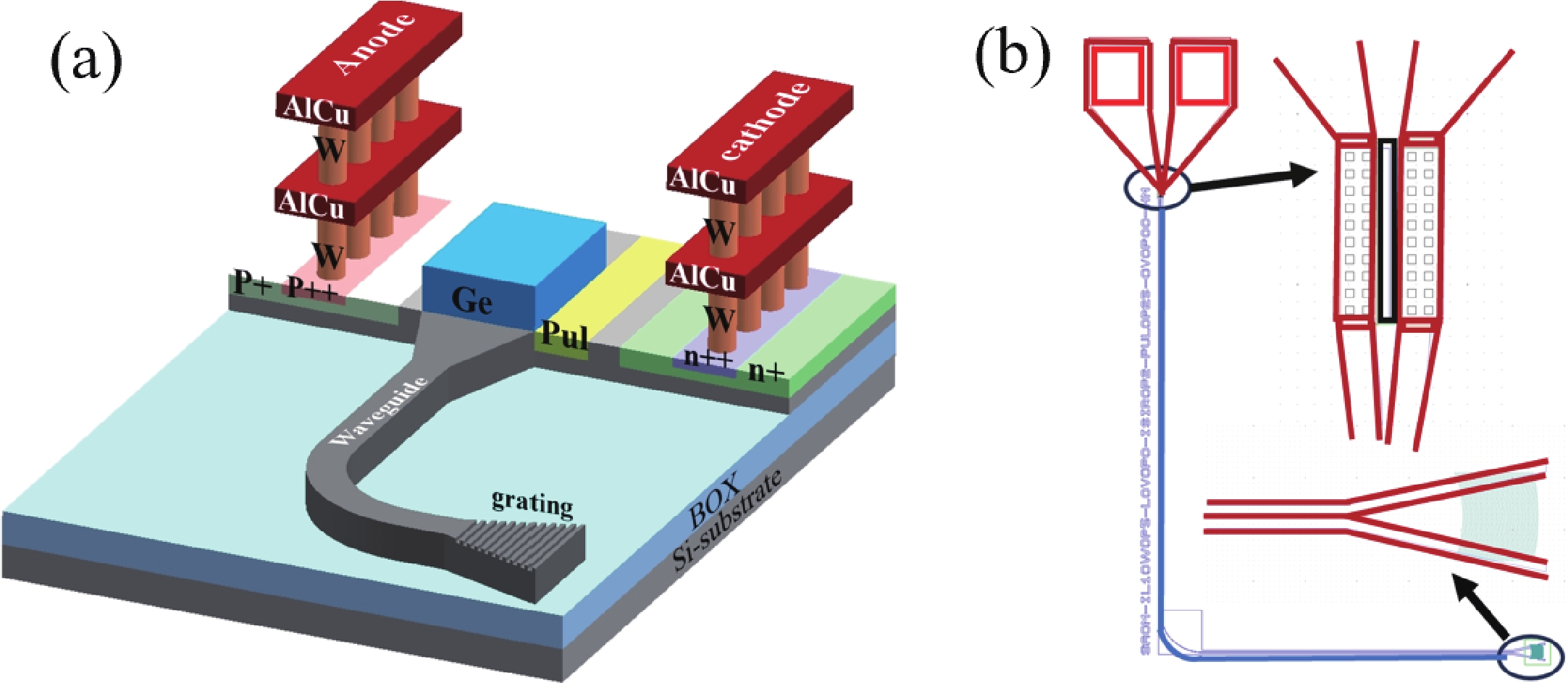
Fig. 1.
(Color online) (a) 3D perspective view for SACM Ge-on-Si APD; (b) top-down perspective of the mask layout in the fabrication process for the device.
ARTICLES
Linkai Yi1, 2, Daoqun Liu1, Wenzheng Cheng1, 2, Daimo Li1, 2, Guoqi Zhou1, 2, Peng Zhang1, Bo Tang1, Bin Li1, Wenwu Wang1, Yan Yang1 and Zhihua Li1,
Corresponding author: Zhihua Li, lizhihua@ime.ac.cn
Abstract: Avalanche photodetectors (APDs) featuring an avalanche multiplication region are vital for reaching high sensitivity and responsivity in optical transceivers. Waveguide-coupled Ge-on-Si separate absorption, charge, and multiplication (SACM) APDs are popular due to their straightforward fabrication process, low optical propagation loss, and high detection sensitivity in optical communications. This paper introduces a lateral SACM Ge-on-Si APD on a silicon-on-insulator (SOI) wafer, featuring a 10 μm-long, 0.5 μm-wide Ge layer at 1310 nm on a standard 8-inch silicon photonics platform. The dark current measures approximately 38.6 μA at −21 V, indicating a breakdown voltage greater than −21 V for the device. The APDs exhibit a unit-gain responsivity of 0.5 A/W at −10 V. At −15 V, their responsivity reaches 2.98 and 2.91 A/W with input powers of −10 and −25 dBm, respectively. The device's 3-dB bandwidth is 15 GHz with an input power of −15 dBm and a gain is 11.68. Experimental results show a peak in impedance at high bias voltages, attributed to inductor and capacitor (LC) circuit resonance, enhancing frequency response. Furthermore, 20 Gbps eye diagrams at −21 V and −9 dBm input power reveal signal to noise ratio (SNRs) of 5.30. This lateral SACM APD, compatible with the stand complementary metal oxide semiconductor (CMOS) process, shows that utilizing the peaking effect at low optical power increases bandwidth.
Key words: photodetectors, optical communications, responsivity, 3-dB bandwidth
| [1] |
Wang B H, Mu J F. High-speed Si-Ge avalanche photodiodes. PhotoniX, 2022, 3, 8 doi: 10.1186/s43074-022-00052-6
|
| [2] |
Liu D Q. Study on the near-infrared COMS compatible avalanche photodetector. PhD Dissertation, University of Chinese Academy of Sciences, 2022 (in Chinese)
|
| [3] |
Smit M, Williams K, van der Tol J. Past, present, and future of InP-based photonic integration. APL Photonics, 2019, 4, 050901 doi: 10.1063/1.5087862
|
| [4] |
Lischke S, Peczek A, Morgan J S, et al. Ultra-fast germanium photodiode with 3-dB bandwidth of 265 GHz. Nat Photon, 2021, 15, 925 doi: 10.1038/s41566-021-00893-w
|
| [5] |
Wu G, Cao H, Jin M, et al. 2×2 SOI optical switch with robust high extinction ratio on all paths enabled by parabolic MMI coupler. 2023 Asia Communications and Photonics Conference/ 2023 International Photonics and Optoelectronics Meetings (ACP/POEM), 2023, 1 doi: 10.1109/ACP/POEM59049.2023.10369772
|
| [6] |
Xia J F, Chen M J, Rizzo A, et al. O-band microring resonator based switch-and-select silicon photonic switch fabric. 2022 Conference on Lasers and Electro-Optics (CLEO), 2022, 1 doi: 10.1364/CLEO_SI.2022.SF4M.7
|
| [7] |
Qian L, Wu D, Liu D, et al. Infrared detector module for airborne hyperspectral LiDAR: Design and demonstration. Appl Opt, 2023, 62, 2161 doi: 10.1364/AO.482626
|
| [8] |
Lin Y X, Ahmad Z, Ou S Y, et al. A 4-D FMCW LiDAR with ultra-high velocity sensitivity. J Lightwave Technol, 2023, 41, 6664 doi: 10.1109/JLT.2023.3292139
|
| [9] |
Liu X B, Li X T, Zhi Z H, et al. Three-electrode germanium-on-silicon avalanche photodiode array. Opt Lett, 2023, 48, 1846 doi: 10.1364/OL.477463
|
| [10] |
Giden I H. Photonic crystal based interferometric design for label-free all-optical sensing applications. Opt Express, 2022, 30, 21679 doi: 10.1364/OE.458772
|
| [11] |
Romijn J, Vollebregt S, Middelburg L M, et al. Integrated 64 pixel UV image sensor and readout in a silicon carbide CMOS technology. Microsyst Nanoeng, 2022, 8, 114 doi: 10.1038/s41378-022-00446-3
|
| [12] |
Lai Y H, Suh M G, Lu Y K, et al. Earth rotation measured by a chip-scale ring laser gyroscope. Nat Photonics, 2020, 14, 345 doi: 10.1038/s41566-020-0588-y
|
| [13] |
Tian Y, Lin Y X, Zheng J Y, et al. 800Gb/s-FR4 specification and interoperability analysis. 2021 Optical Fiber Communications Conference and Exhibition (OFC), 2021, 1 doi: 10.1364/OFC.2021.W7F.6
|
| [14] |
Potet J, Simon G, Gaillard G, et al. Uncooled high speed Ge/Si avalanche photodiode for 50 Gbit/s-PON with 60 km reach. Optical Fiber Communication Conference (OFC) 2023, 2023, 1 doi: 10.1364/OFC.2023.Th3G.3
|
| [15] |
Assefa S, Xia F N, Vlasov Y A. Reinventing germanium avalanche photodetector for nanophotonic on-chip optical interconnects. Nature, 2010, 464, 80 doi: 10.1038/nature08813
|
| [16] |
Assefa S, Xia F N, Bedell S W, et al. CMOS-integrated high-speed MSM germanium waveguide photodetector. Opt Express, 2010, 18, 4986 doi: 10.1364/OE.18.004986
|
| [17] |
Benedikovic D, Virot L, Aubin G, et al. 25 Gbps low-voltage hetero-structured silicon-germanium waveguide pin photodetectors for monolithic on-chip nanophotonic architectures. Photon Res, 2019, 7, 437 doi: 10.1364/PRJ.7.000437
|
| [18] |
Benedikovic D, Virot L, Aubin G, et al. Comprehensive study on chip-integrated germanium pin photodetectors for energy-efficient silicon interconnects. IEEE J Quantum Electron, 2020, 56, 8400409 doi: 10.1109/JQE.2019.2954355
|
| [19] |
Campbell J C. Recent advances in avalanche photodiodes. J Light Technol, 2016, 34, 278 doi: 10.1109/JLT.2015.2453092
|
| [20] |
Wang B H, Huang Z H, Zeng X G, et al. A compact model for Si—Ge avalanche photodiodes. 2018 IEEE 15th International Conference on Group IV Photonics (GFP). Cancun, Mexico. IEEE, 2018, 1 doi: 10.1109/GROUP4.2018.8478743
|
| [21] |
Wang B H, Huang Z H, Zeng X G, et al. 35Gb/s ultralow-voltage three-terminal Si-Ge avalanche photodiode. Optical Fiber Communication Conference (OFC) 2019, 2019, 1
|
| [22] |
Zeng X G, Huang Z H, Wang B H, et al. Silicon–germanium avalanche photodiodes with direct control of electric field in charge multiplication region. Optica, 2019, 6, 772 doi: 10.1364/OPTICA.6.000772
|
| [23] |
Samani A, Carpentier O, El-Fiky E, et al. Highly sensitive, 112 gb/s O-band waveguide coupled silicon-germanium avalanche photodetectors. 2019 Optical Fiber Communications Conference and Exhibition (OFC). San Diego, CA, USA. IEEE, 2019, 1
|
| [24] |
Huang M Y, Cai P F, Li S, et al. 56GHz waveguide Ge/Si avalanche photodiode. Optical Fiber Communication Conference, 2018, 1
|
| [25] |
Zeng Q Y, Pan Z X, Zeng Z H, et al. Space charge effects on the bandwidth of Ge/Si avalanche photodetectors. Semicond Sci Technol, 2020, 35, 035026 doi: 10.1088/1361-6641/ab7147
|
| [26] |
Zhang J Q, Lin H M, Liu M, et al. Research on the leakage current at sidewall of mesa Ge/Si avalanche photodiode. AIP Adv, 2021, 11, 075320 doi: 10.1063/5.0054242
|
| [27] |
Huang Z H, Li C, Liang D, et al. 25 Gbps low-voltage waveguide Si–Ge avalanche photodiode. Optica, 2016, 3, 793 doi: 10.1364/OPTICA.3.000793
|
| [28] |
Wang B H, Huang Z H, Zeng X G, et al. A compact model for Si-Ge avalanche photodiodes over a wide range of multiplication gain. J Light Technol, 2019, 37, 3229 doi: 10.1109/JLT.2019.2913179
|
| [29] |
Srinivasan S A, Berciano M, De Heyn P, et al. 27 GHz silicon-contacted waveguide-coupled Ge/Si avalanche photodiode. J Light Technol, 2020, 38, 3044 doi: 10.1109/JLT.2020.2986923
|
| [30] |
Srinivasan S A, Lambrecht J, Guermandi D, et al. 56 gb/s NRZ O-band hybrid BiCMOS-silicon photonics receiver using Ge/si avalanche photodiode. J Lightwave Technol, 2021, 39, 1409 doi: 10.1109/JLT.2020.3038361
|
| [31] |
Xiang Y L, Cao H Z, Liu C Y, et al. High-performance waveguide Ge/Si avalanche photodiode with a lateral separate-absorption-charge-multiplication structure. Opt Express, 2022, 30, 11288 doi: 10.1364/OE.450618
|
| [32] |
Xiang Y L, Cao H Z, Liu C Y, et al. High-speed waveguide Ge/Si avalanche photodiode with a gain-bandwidth product of 615 GHz. Optica, 2022, 9, 762 doi: 10.1364/OPTICA.462609
|
| [33] |
Li X L, Zhu Y P, Liu Z, et al. 75 GHz germanium waveguide photodetector with 64 Gbps data rates utilizing an inductive-gain-peaking technique. J Semicond, 2023, 44, 012301 doi: 10.1088/1674-4926/44/1/012301
|
| [34] |
Peng Y W, Yuan Y, Sorin W V, et al. Demonstration of an ultra-high-responsivity all-silicon avalanche photodetectors. 2023 Optical Fiber Communications Conference and Exhibition (OFC). San Diego, CA, USA, 2023, 1 doi: 10.1364/OFC.2023.W1A.2
|
| [35] |
Zhang J S, Xu H W, Tan K H, et al. First Si-waveguide-integrated InGaAs/InAlAs avalanche photodiodes on SOI platform. 2022 IEEE Symposium on VLSI Technology and Circuits (VLSI Technology and Circuits). Honolulu, HI, USA, 2022, 409 doi: 10.1109/VLSITechnologyandCir46769.2022.9830481
|
| [36] |
Decker D R, Dunn C N. Determination of germanium ionization coefficients from small-signal IMPATT diode characteristics. IEEE Trans Electron Devices, 1970, 17, 290 doi: 10.1109/T-ED.1970.16972
|
| [37] |
Chen H T, Verheyen P, De Heyn P, et al. High-responsivity low-voltage 28-gb/s Ge p-i-n photodetector with silicon contacts. J Lightwave Technol, 2015, 33, 820 doi: 10.1109/JLT.2014.2367134
|
| [38] |
Bellegarde C, Pargon E, Sciancalepore C, et al. Optimization of H2 thermal annealing process for the fabrication of ultra-low loss sub-micron silicon-on-insulator rib waveguides. Silicon Photonics XIII. San Francisco, USA. SPIE, 2018, 1 doi: 10.1117/12.2289564
|
| [39] |
Bellegarde C, Pargon E, Sciancalepore C, et al. Improvement of sidewall roughness of sub-micron silicon-on-insulator waveguides for low-loss on-chip links. Silicon Photonics XII, 2017, 10108, 1010816 doi: 10.1117/12.2250344
|
| [40] |
Michel J, Liu J F, Kimerling L C. High-performance Ge-on-Si photodetectors. Nature Photon, 2010, 4, 527 doi: 10.1038/nphoton.2010.157
|
| [41] |
Lee K H, Bao S Y, Chong G Y, et al. Defects reduction of Ge epitaxial film in a germanium-on-insulator wafer by annealing in oxygen ambient. APL Mater, 2015, 3, 016102 doi: 10.1063/1.4905487
|
| [42] |
Hu X, Zhang H G, Wu D Y, et al. High-performance germanium avalanche photodetector for 100 Gbit/s photonics receivers. Opt Lett, 2021, 46, 3837 doi: 10.1364/OL.433694
|
| [43] |
Benedikovic D, Virot L, Aubin G, et al. 40 Gbps heterostructure germanium avalanche photo receiver on a silicon chip. Optica, 2020, 7, 775 doi: 10.1364/OPTICA.393537
|
| [44] |
Filippov V, Mitsuk S, Vlasov A, et al. Modelling of deformations and band diagram of semiconductor hetorostructure silicon-germanium. 2023 5th International Conference on Control Systems, Mathematical Modeling, Automation and Energy Efficiency (SUMMA). Lipetsk, Russian Federation, 2023, 1081 doi: 10.1109/SUMMA60232.2023.10349379
|
| [45] |
Reboud V, Gassenq A, Hartmann J M, et al. Germanium based photonic components toward a full silicon/germanium photonic platform. Prog Cryst Growth Charact Mater, 2017, 63, 1 doi: 10.1016/j.pcrysgrow.2017.04.004
|
| [46] |
Rockwell A K, Yuan Y, Jones A H, et al. Al0.8In0.2As0.23Sb0.77 avalanche photodiodes. IEEE Photon Technol Lett, 2018, 30, 1048 doi: 10.1109/LPT.2018.2826999
|
| [47] |
Liu D Q, Zhang P, Tang B, et al. High-performance waveguide-integrated Ge/Si avalanche photodetector with lateral multiplication region. Micromachines, 2022, 13, 649 doi: 10.3390/mi13050649
|
| [48] |
Yi L K, Liu D Q, Li D M, et al. Waveguide-integrated Ge/Si avalanche photodiode with vertical multiplication region for 1310 nm detection. Photonics, 2023, 10, 750 doi: 10.3390/photonics10070750
|
| [49] |
Yuan Y, Huang Z H, Zeng X G, et al. High responsivity Si-Ge waveguide avalanche photodiodes enhanced by loop reflector. IEEE J Sel Top Quantum Electron, 2022, 28, 1 doi: 10.1109/JSTQE.2022.3206066
|
| [50] |
Emmons R B. Avalanche-photodiode frequency response. J Appl Phys, 1967, 38, 3705 doi: 10.1063/1.1710199
|
| [51] |
Dai D X, Rodwell M J W, Bowers J E, et al. Derivation of the small signal response and equivalent circuit model for a separate absorption and multiplication layer avalanche photodetector. IEEE J Sel Top Quantum Electron, 2010, 16, 1328 doi: 10.1109/JSTQE.2009.2038497
|
| [52] |
Duan N, Liow T Y, Lim A E J, et al. 310 GHz gain-bandwidth product Ge/Si avalanche photodetector for 1550 nm light detection. Opt Express, 2012, 20, 11031 doi: 10.1364/OE.20.011031
|
| [53] |
Huang M Y, Magruder K, Malinge Y, et al. Recess-type waveguide integrated germanium on silicon avalanche photodiode. Optical Fiber Communication Conference (OFC) 2021, 2021, 1 doi: 10.1364/OFC.2021.F2C.3
|
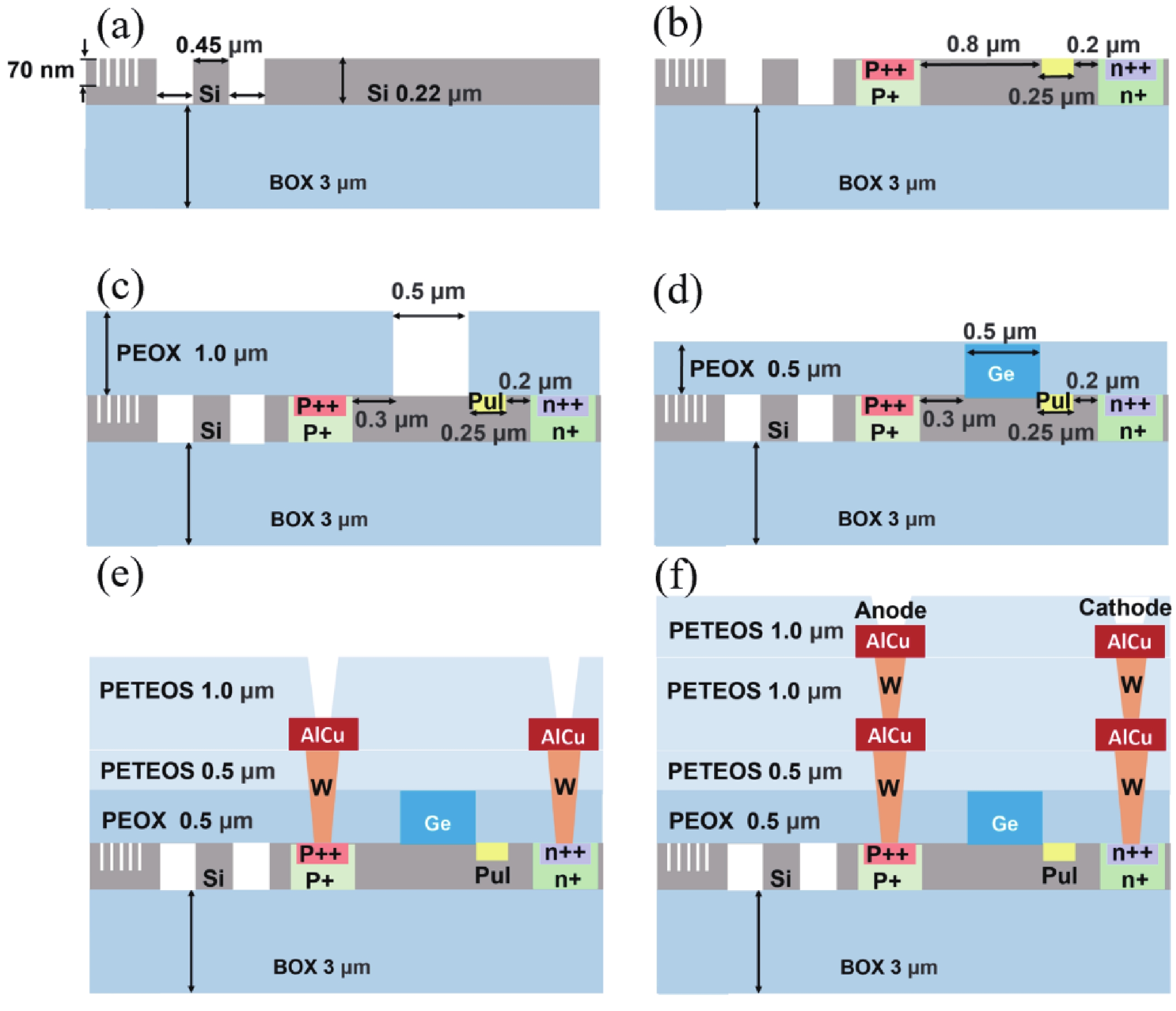
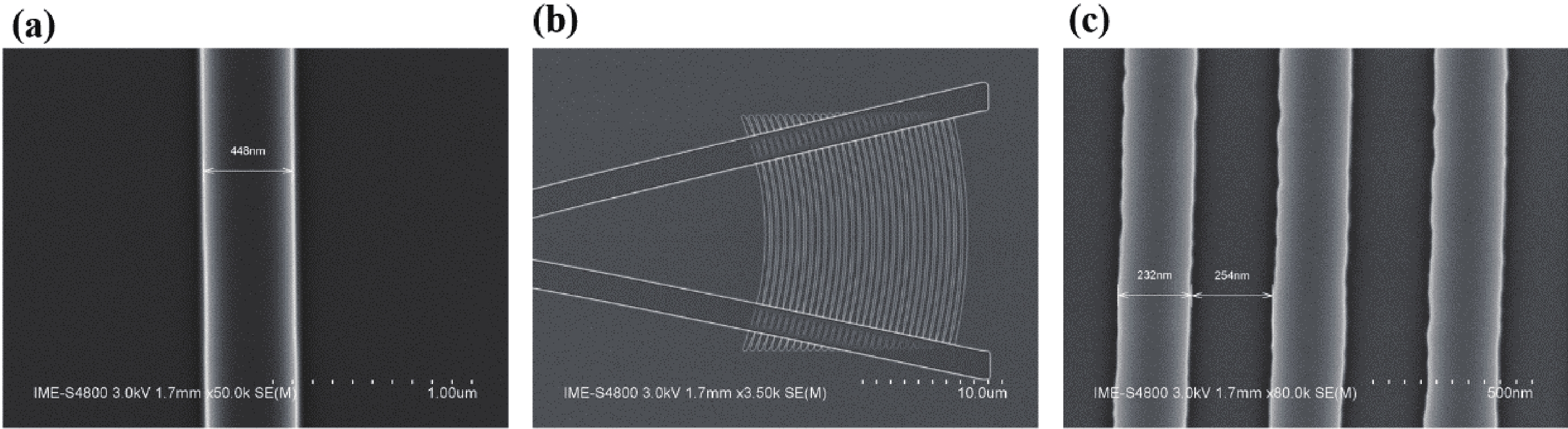
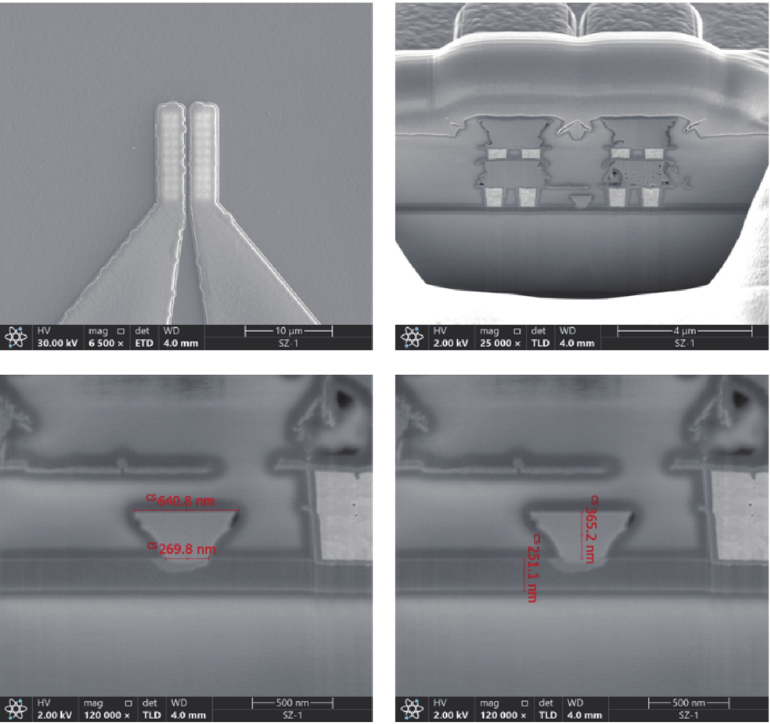
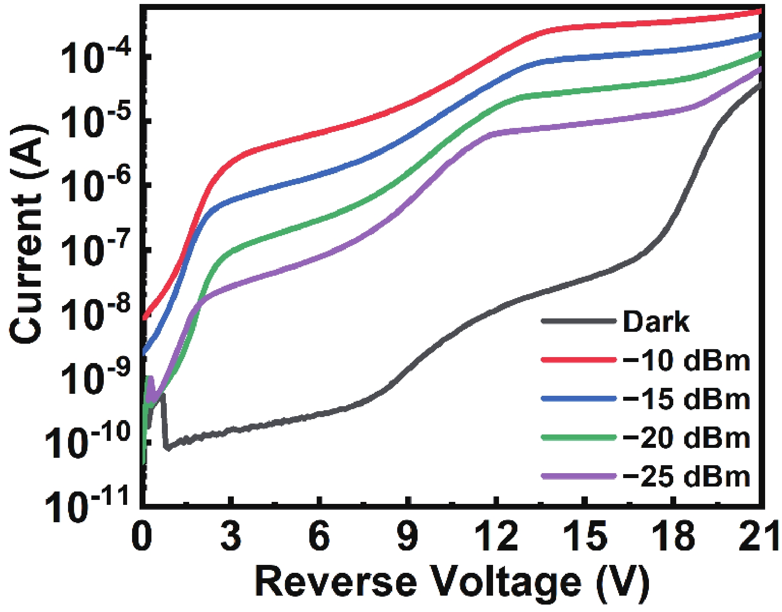
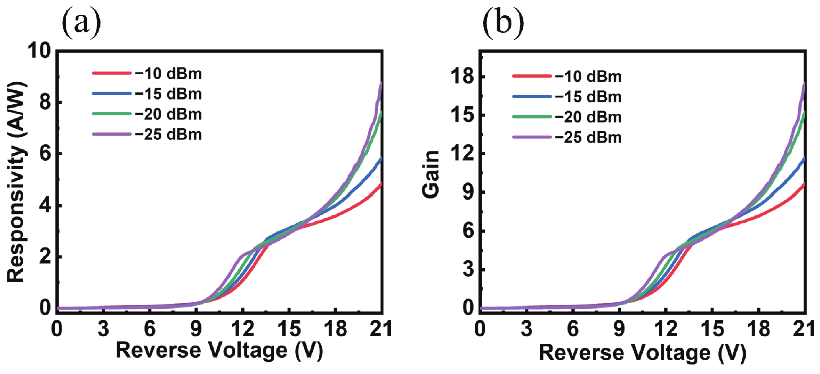
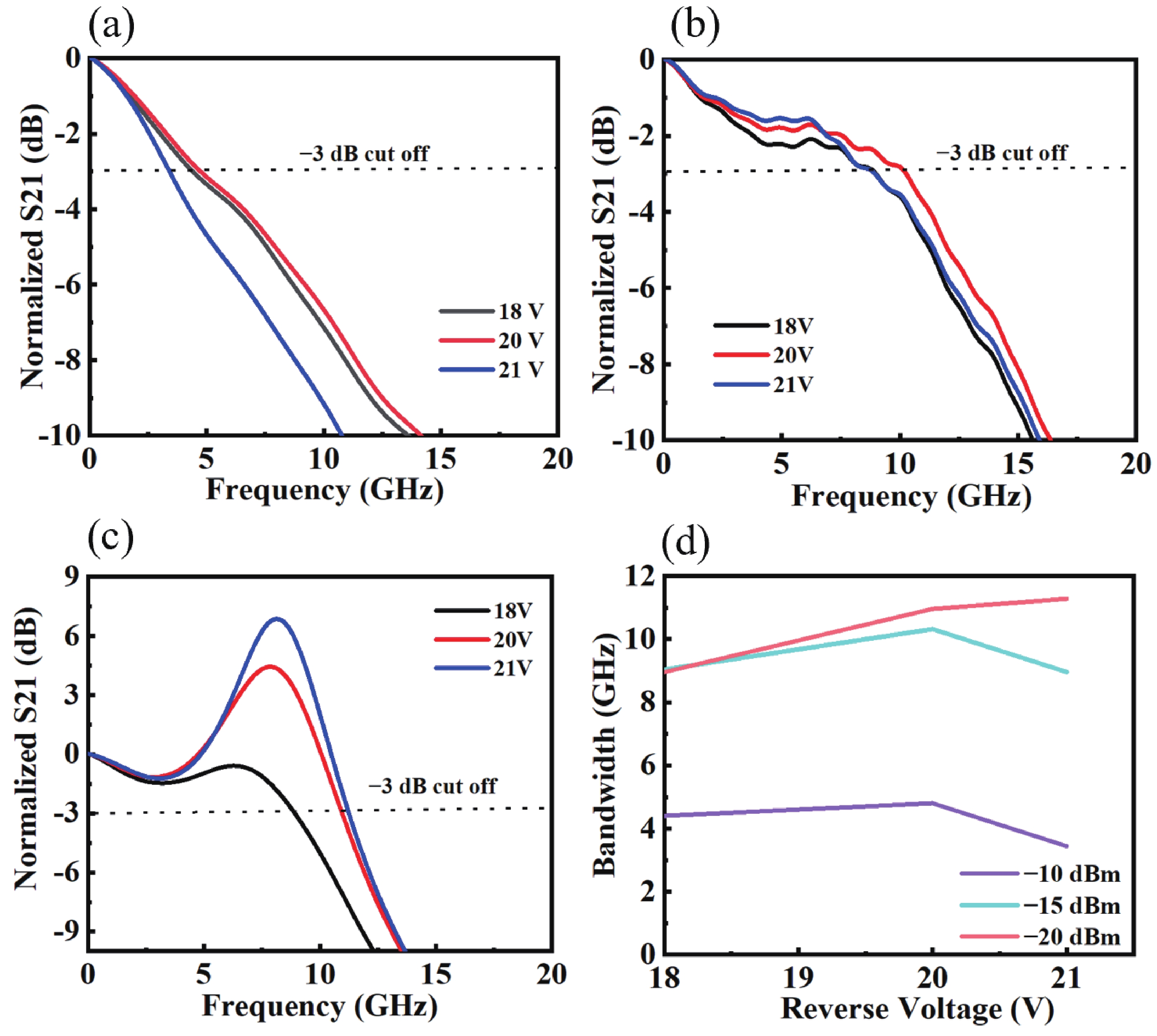
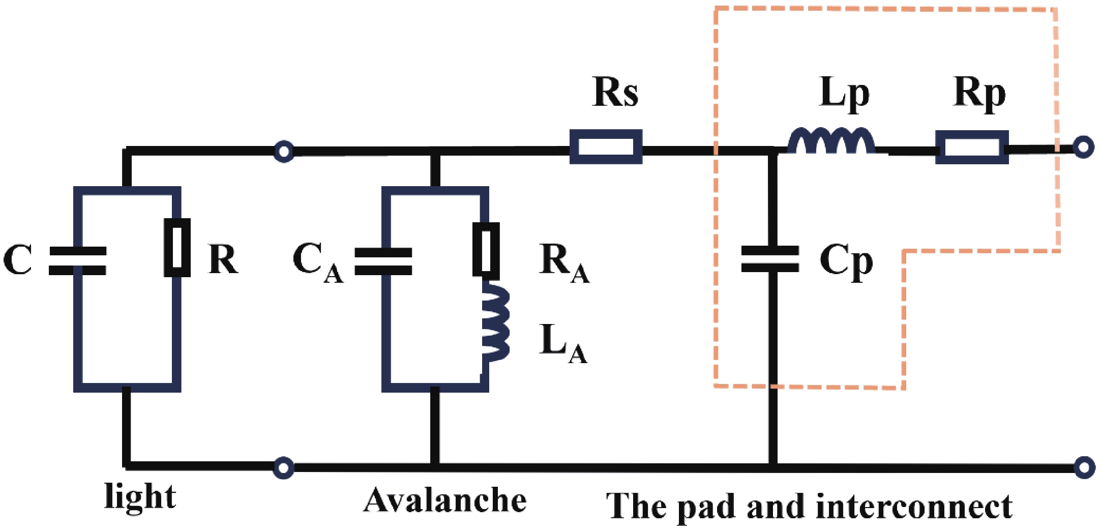
Table 1. Benchmarking table of the waveguide Ge-on-Si APDs.
| Type | PN type |
Λ (nm) |
Id (nA) |
R0 (A/W) |
Bandwidth (GHz) |
Peak value |
Year |
| Surface illuminated | Vertical SACM | 1550 | 30 | 0.30 | 8.0 | / | 2012[52] |
| Waveguide | Lateral PIN | 1550 | 600 | 0.49 | 33 | / | 2020[43] |
| Waveguide | Vertical PIN | 1550 | 20 | 0.8 | 21.0 | / | 2021[44] |
| Waveguide | Lateral SACM | 1310 | ~30 | 0.65 | 22.7 | / | 2021[30] |
| Waveguide | Vertical SACM | 1310 | 1 | 0.75 | 29.5 | / | 2021[53] |
| Waveguide | Lateral RT | 1310 | ~100 | 0.93 | 48.0 | / | 2022[32] |
| Waveguide | Vertical | 1550 | 35 | 0.81 | >75 | <3 | 2023[33] |
| Waveguide | Lateral SACM | 1310 | 38.6 | 0.5 | 15 | >6 | This work |
| Note: “/” indicates that the article does not mention this parameter. | |||||||
 DownLoad: CSV
| [1] |
Wang B H, Mu J F. High-speed Si-Ge avalanche photodiodes. PhotoniX, 2022, 3, 8 doi: 10.1186/s43074-022-00052-6
|
| [2] |
Liu D Q. Study on the near-infrared COMS compatible avalanche photodetector. PhD Dissertation, University of Chinese Academy of Sciences, 2022 (in Chinese)
|
| [3] |
Smit M, Williams K, van der Tol J. Past, present, and future of InP-based photonic integration. APL Photonics, 2019, 4, 050901 doi: 10.1063/1.5087862
|
| [4] |
Lischke S, Peczek A, Morgan J S, et al. Ultra-fast germanium photodiode with 3-dB bandwidth of 265 GHz. Nat Photon, 2021, 15, 925 doi: 10.1038/s41566-021-00893-w
|
| [5] |
Wu G, Cao H, Jin M, et al. 2×2 SOI optical switch with robust high extinction ratio on all paths enabled by parabolic MMI coupler. 2023 Asia Communications and Photonics Conference/ 2023 International Photonics and Optoelectronics Meetings (ACP/POEM), 2023, 1 doi: 10.1109/ACP/POEM59049.2023.10369772
|
| [6] |
Xia J F, Chen M J, Rizzo A, et al. O-band microring resonator based switch-and-select silicon photonic switch fabric. 2022 Conference on Lasers and Electro-Optics (CLEO), 2022, 1 doi: 10.1364/CLEO_SI.2022.SF4M.7
|
| [7] |
Qian L, Wu D, Liu D, et al. Infrared detector module for airborne hyperspectral LiDAR: Design and demonstration. Appl Opt, 2023, 62, 2161 doi: 10.1364/AO.482626
|
| [8] |
Lin Y X, Ahmad Z, Ou S Y, et al. A 4-D FMCW LiDAR with ultra-high velocity sensitivity. J Lightwave Technol, 2023, 41, 6664 doi: 10.1109/JLT.2023.3292139
|
| [9] |
Liu X B, Li X T, Zhi Z H, et al. Three-electrode germanium-on-silicon avalanche photodiode array. Opt Lett, 2023, 48, 1846 doi: 10.1364/OL.477463
|
| [10] |
Giden I H. Photonic crystal based interferometric design for label-free all-optical sensing applications. Opt Express, 2022, 30, 21679 doi: 10.1364/OE.458772
|
| [11] |
Romijn J, Vollebregt S, Middelburg L M, et al. Integrated 64 pixel UV image sensor and readout in a silicon carbide CMOS technology. Microsyst Nanoeng, 2022, 8, 114 doi: 10.1038/s41378-022-00446-3
|
| [12] |
Lai Y H, Suh M G, Lu Y K, et al. Earth rotation measured by a chip-scale ring laser gyroscope. Nat Photonics, 2020, 14, 345 doi: 10.1038/s41566-020-0588-y
|
| [13] |
Tian Y, Lin Y X, Zheng J Y, et al. 800Gb/s-FR4 specification and interoperability analysis. 2021 Optical Fiber Communications Conference and Exhibition (OFC), 2021, 1 doi: 10.1364/OFC.2021.W7F.6
|
| [14] |
Potet J, Simon G, Gaillard G, et al. Uncooled high speed Ge/Si avalanche photodiode for 50 Gbit/s-PON with 60 km reach. Optical Fiber Communication Conference (OFC) 2023, 2023, 1 doi: 10.1364/OFC.2023.Th3G.3
|
| [15] |
Assefa S, Xia F N, Vlasov Y A. Reinventing germanium avalanche photodetector for nanophotonic on-chip optical interconnects. Nature, 2010, 464, 80 doi: 10.1038/nature08813
|
| [16] |
Assefa S, Xia F N, Bedell S W, et al. CMOS-integrated high-speed MSM germanium waveguide photodetector. Opt Express, 2010, 18, 4986 doi: 10.1364/OE.18.004986
|
| [17] |
Benedikovic D, Virot L, Aubin G, et al. 25 Gbps low-voltage hetero-structured silicon-germanium waveguide pin photodetectors for monolithic on-chip nanophotonic architectures. Photon Res, 2019, 7, 437 doi: 10.1364/PRJ.7.000437
|
| [18] |
Benedikovic D, Virot L, Aubin G, et al. Comprehensive study on chip-integrated germanium pin photodetectors for energy-efficient silicon interconnects. IEEE J Quantum Electron, 2020, 56, 8400409 doi: 10.1109/JQE.2019.2954355
|
| [19] |
Campbell J C. Recent advances in avalanche photodiodes. J Light Technol, 2016, 34, 278 doi: 10.1109/JLT.2015.2453092
|
| [20] |
Wang B H, Huang Z H, Zeng X G, et al. A compact model for Si—Ge avalanche photodiodes. 2018 IEEE 15th International Conference on Group IV Photonics (GFP). Cancun, Mexico. IEEE, 2018, 1 doi: 10.1109/GROUP4.2018.8478743
|
| [21] |
Wang B H, Huang Z H, Zeng X G, et al. 35Gb/s ultralow-voltage three-terminal Si-Ge avalanche photodiode. Optical Fiber Communication Conference (OFC) 2019, 2019, 1
|
| [22] |
Zeng X G, Huang Z H, Wang B H, et al. Silicon–germanium avalanche photodiodes with direct control of electric field in charge multiplication region. Optica, 2019, 6, 772 doi: 10.1364/OPTICA.6.000772
|
| [23] |
Samani A, Carpentier O, El-Fiky E, et al. Highly sensitive, 112 gb/s O-band waveguide coupled silicon-germanium avalanche photodetectors. 2019 Optical Fiber Communications Conference and Exhibition (OFC). San Diego, CA, USA. IEEE, 2019, 1
|
| [24] |
Huang M Y, Cai P F, Li S, et al. 56GHz waveguide Ge/Si avalanche photodiode. Optical Fiber Communication Conference, 2018, 1
|
| [25] |
Zeng Q Y, Pan Z X, Zeng Z H, et al. Space charge effects on the bandwidth of Ge/Si avalanche photodetectors. Semicond Sci Technol, 2020, 35, 035026 doi: 10.1088/1361-6641/ab7147
|
| [26] |
Zhang J Q, Lin H M, Liu M, et al. Research on the leakage current at sidewall of mesa Ge/Si avalanche photodiode. AIP Adv, 2021, 11, 075320 doi: 10.1063/5.0054242
|
| [27] |
Huang Z H, Li C, Liang D, et al. 25 Gbps low-voltage waveguide Si–Ge avalanche photodiode. Optica, 2016, 3, 793 doi: 10.1364/OPTICA.3.000793
|
| [28] |
Wang B H, Huang Z H, Zeng X G, et al. A compact model for Si-Ge avalanche photodiodes over a wide range of multiplication gain. J Light Technol, 2019, 37, 3229 doi: 10.1109/JLT.2019.2913179
|
| [29] |
Srinivasan S A, Berciano M, De Heyn P, et al. 27 GHz silicon-contacted waveguide-coupled Ge/Si avalanche photodiode. J Light Technol, 2020, 38, 3044 doi: 10.1109/JLT.2020.2986923
|
| [30] |
Srinivasan S A, Lambrecht J, Guermandi D, et al. 56 gb/s NRZ O-band hybrid BiCMOS-silicon photonics receiver using Ge/si avalanche photodiode. J Lightwave Technol, 2021, 39, 1409 doi: 10.1109/JLT.2020.3038361
|
| [31] |
Xiang Y L, Cao H Z, Liu C Y, et al. High-performance waveguide Ge/Si avalanche photodiode with a lateral separate-absorption-charge-multiplication structure. Opt Express, 2022, 30, 11288 doi: 10.1364/OE.450618
|
| [32] |
Xiang Y L, Cao H Z, Liu C Y, et al. High-speed waveguide Ge/Si avalanche photodiode with a gain-bandwidth product of 615 GHz. Optica, 2022, 9, 762 doi: 10.1364/OPTICA.462609
|
| [33] |
Li X L, Zhu Y P, Liu Z, et al. 75 GHz germanium waveguide photodetector with 64 Gbps data rates utilizing an inductive-gain-peaking technique. J Semicond, 2023, 44, 012301 doi: 10.1088/1674-4926/44/1/012301
|
| [34] |
Peng Y W, Yuan Y, Sorin W V, et al. Demonstration of an ultra-high-responsivity all-silicon avalanche photodetectors. 2023 Optical Fiber Communications Conference and Exhibition (OFC). San Diego, CA, USA, 2023, 1 doi: 10.1364/OFC.2023.W1A.2
|
| [35] |
Zhang J S, Xu H W, Tan K H, et al. First Si-waveguide-integrated InGaAs/InAlAs avalanche photodiodes on SOI platform. 2022 IEEE Symposium on VLSI Technology and Circuits (VLSI Technology and Circuits). Honolulu, HI, USA, 2022, 409 doi: 10.1109/VLSITechnologyandCir46769.2022.9830481
|
| [36] |
Decker D R, Dunn C N. Determination of germanium ionization coefficients from small-signal IMPATT diode characteristics. IEEE Trans Electron Devices, 1970, 17, 290 doi: 10.1109/T-ED.1970.16972
|
| [37] |
Chen H T, Verheyen P, De Heyn P, et al. High-responsivity low-voltage 28-gb/s Ge p-i-n photodetector with silicon contacts. J Lightwave Technol, 2015, 33, 820 doi: 10.1109/JLT.2014.2367134
|
| [38] |
Bellegarde C, Pargon E, Sciancalepore C, et al. Optimization of H2 thermal annealing process for the fabrication of ultra-low loss sub-micron silicon-on-insulator rib waveguides. Silicon Photonics XIII. San Francisco, USA. SPIE, 2018, 1 doi: 10.1117/12.2289564
|
| [39] |
Bellegarde C, Pargon E, Sciancalepore C, et al. Improvement of sidewall roughness of sub-micron silicon-on-insulator waveguides for low-loss on-chip links. Silicon Photonics XII, 2017, 10108, 1010816 doi: 10.1117/12.2250344
|
| [40] |
Michel J, Liu J F, Kimerling L C. High-performance Ge-on-Si photodetectors. Nature Photon, 2010, 4, 527 doi: 10.1038/nphoton.2010.157
|
| [41] |
Lee K H, Bao S Y, Chong G Y, et al. Defects reduction of Ge epitaxial film in a germanium-on-insulator wafer by annealing in oxygen ambient. APL Mater, 2015, 3, 016102 doi: 10.1063/1.4905487
|
| [42] |
Hu X, Zhang H G, Wu D Y, et al. High-performance germanium avalanche photodetector for 100 Gbit/s photonics receivers. Opt Lett, 2021, 46, 3837 doi: 10.1364/OL.433694
|
| [43] |
Benedikovic D, Virot L, Aubin G, et al. 40 Gbps heterostructure germanium avalanche photo receiver on a silicon chip. Optica, 2020, 7, 775 doi: 10.1364/OPTICA.393537
|
| [44] |
Filippov V, Mitsuk S, Vlasov A, et al. Modelling of deformations and band diagram of semiconductor hetorostructure silicon-germanium. 2023 5th International Conference on Control Systems, Mathematical Modeling, Automation and Energy Efficiency (SUMMA). Lipetsk, Russian Federation, 2023, 1081 doi: 10.1109/SUMMA60232.2023.10349379
|
| [45] |
Reboud V, Gassenq A, Hartmann J M, et al. Germanium based photonic components toward a full silicon/germanium photonic platform. Prog Cryst Growth Charact Mater, 2017, 63, 1 doi: 10.1016/j.pcrysgrow.2017.04.004
|
| [46] |
Rockwell A K, Yuan Y, Jones A H, et al. Al0.8In0.2As0.23Sb0.77 avalanche photodiodes. IEEE Photon Technol Lett, 2018, 30, 1048 doi: 10.1109/LPT.2018.2826999
|
| [47] |
Liu D Q, Zhang P, Tang B, et al. High-performance waveguide-integrated Ge/Si avalanche photodetector with lateral multiplication region. Micromachines, 2022, 13, 649 doi: 10.3390/mi13050649
|
| [48] |
Yi L K, Liu D Q, Li D M, et al. Waveguide-integrated Ge/Si avalanche photodiode with vertical multiplication region for 1310 nm detection. Photonics, 2023, 10, 750 doi: 10.3390/photonics10070750
|
| [49] |
Yuan Y, Huang Z H, Zeng X G, et al. High responsivity Si-Ge waveguide avalanche photodiodes enhanced by loop reflector. IEEE J Sel Top Quantum Electron, 2022, 28, 1 doi: 10.1109/JSTQE.2022.3206066
|
| [50] |
Emmons R B. Avalanche-photodiode frequency response. J Appl Phys, 1967, 38, 3705 doi: 10.1063/1.1710199
|
| [51] |
Dai D X, Rodwell M J W, Bowers J E, et al. Derivation of the small signal response and equivalent circuit model for a separate absorption and multiplication layer avalanche photodetector. IEEE J Sel Top Quantum Electron, 2010, 16, 1328 doi: 10.1109/JSTQE.2009.2038497
|
| [52] |
Duan N, Liow T Y, Lim A E J, et al. 310 GHz gain-bandwidth product Ge/Si avalanche photodetector for 1550 nm light detection. Opt Express, 2012, 20, 11031 doi: 10.1364/OE.20.011031
|
| [53] |
Huang M Y, Magruder K, Malinge Y, et al. Recess-type waveguide integrated germanium on silicon avalanche photodiode. Optical Fiber Communication Conference (OFC) 2021, 2021, 1 doi: 10.1364/OFC.2021.F2C.3
|


Article views: 160 Times PDF downloads: 50 Times Cited by: 0 Times
Received: 19 February 2024 Revised: 14 March 2024 Online: Accepted Manuscript: 25 March 2024Uncorrected proof: 26 March 2024
| Citation: |
Linkai Yi, Daoqun Liu, Wenzheng Cheng, Daimo Li, Guoqi Zhou, Peng Zhang, Bo Tang, Bin Li, Wenwu Wang, Yan Yang, Zhihua Li. A peak enhancement of frequency response of waveguide integrated silicon-based germanium avalanche photodetector[J]. Journal of Semiconductors, 2024, 45(7): 072401. doi: 10.1088/1674-4926/24020006
L K Yi, D Q Liu, W Z Cheng, D M Li, G Q Zhou, P Zhang, B Tang, B Li, W W Wang, Y Yang, and Z H Li, A peak enhancement of frequency response of waveguide integrated silicon-based germanium avalanche photodetector[J]. J. Semicond., 2024, 45(7), 072401 doi: 10.1088/1674-4926/24020006
Export: BibTex EndNote

|
| [1] |
Wang B H, Mu J F. High-speed Si-Ge avalanche photodiodes. PhotoniX, 2022, 3, 8 doi: 10.1186/s43074-022-00052-6
|
| [2] |
Liu D Q. Study on the near-infrared COMS compatible avalanche photodetector. PhD Dissertation, University of Chinese Academy of Sciences, 2022 (in Chinese)
|
| [3] |
Smit M, Williams K, van der Tol J. Past, present, and future of InP-based photonic integration. APL Photonics, 2019, 4, 050901 doi: 10.1063/1.5087862
|
| [4] |
Lischke S, Peczek A, Morgan J S, et al. Ultra-fast germanium photodiode with 3-dB bandwidth of 265 GHz. Nat Photon, 2021, 15, 925 doi: 10.1038/s41566-021-00893-w
|
| [5] |
Wu G, Cao H, Jin M, et al. 2×2 SOI optical switch with robust high extinction ratio on all paths enabled by parabolic MMI coupler. 2023 Asia Communications and Photonics Conference/ 2023 International Photonics and Optoelectronics Meetings (ACP/POEM), 2023, 1 doi: 10.1109/ACP/POEM59049.2023.10369772
|
| [6] |
Xia J F, Chen M J, Rizzo A, et al. O-band microring resonator based switch-and-select silicon photonic switch fabric. 2022 Conference on Lasers and Electro-Optics (CLEO), 2022, 1 doi: 10.1364/CLEO_SI.2022.SF4M.7
|
| [7] |
Qian L, Wu D, Liu D, et al. Infrared detector module for airborne hyperspectral LiDAR: Design and demonstration. Appl Opt, 2023, 62, 2161 doi: 10.1364/AO.482626
|
| [8] |
Lin Y X, Ahmad Z, Ou S Y, et al. A 4-D FMCW LiDAR with ultra-high velocity sensitivity. J Lightwave Technol, 2023, 41, 6664 doi: 10.1109/JLT.2023.3292139
|
| [9] |
Liu X B, Li X T, Zhi Z H, et al. Three-electrode germanium-on-silicon avalanche photodiode array. Opt Lett, 2023, 48, 1846 doi: 10.1364/OL.477463
|
| [10] |
Giden I H. Photonic crystal based interferometric design for label-free all-optical sensing applications. Opt Express, 2022, 30, 21679 doi: 10.1364/OE.458772
|
| [11] |
Romijn J, Vollebregt S, Middelburg L M, et al. Integrated 64 pixel UV image sensor and readout in a silicon carbide CMOS technology. Microsyst Nanoeng, 2022, 8, 114 doi: 10.1038/s41378-022-00446-3
|
| [12] |
Lai Y H, Suh M G, Lu Y K, et al. Earth rotation measured by a chip-scale ring laser gyroscope. Nat Photonics, 2020, 14, 345 doi: 10.1038/s41566-020-0588-y
|
| [13] |
Tian Y, Lin Y X, Zheng J Y, et al. 800Gb/s-FR4 specification and interoperability analysis. 2021 Optical Fiber Communications Conference and Exhibition (OFC), 2021, 1 doi: 10.1364/OFC.2021.W7F.6
|
| [14] |
Potet J, Simon G, Gaillard G, et al. Uncooled high speed Ge/Si avalanche photodiode for 50 Gbit/s-PON with 60 km reach. Optical Fiber Communication Conference (OFC) 2023, 2023, 1 doi: 10.1364/OFC.2023.Th3G.3
|
| [15] |
Assefa S, Xia F N, Vlasov Y A. Reinventing germanium avalanche photodetector for nanophotonic on-chip optical interconnects. Nature, 2010, 464, 80 doi: 10.1038/nature08813
|
| [16] |
Assefa S, Xia F N, Bedell S W, et al. CMOS-integrated high-speed MSM germanium waveguide photodetector. Opt Express, 2010, 18, 4986 doi: 10.1364/OE.18.004986
|
| [17] |
Benedikovic D, Virot L, Aubin G, et al. 25 Gbps low-voltage hetero-structured silicon-germanium waveguide pin photodetectors for monolithic on-chip nanophotonic architectures. Photon Res, 2019, 7, 437 doi: 10.1364/PRJ.7.000437
|
| [18] |
Benedikovic D, Virot L, Aubin G, et al. Comprehensive study on chip-integrated germanium pin photodetectors for energy-efficient silicon interconnects. IEEE J Quantum Electron, 2020, 56, 8400409 doi: 10.1109/JQE.2019.2954355
|
| [19] |
Campbell J C. Recent advances in avalanche photodiodes. J Light Technol, 2016, 34, 278 doi: 10.1109/JLT.2015.2453092
|
| [20] |
Wang B H, Huang Z H, Zeng X G, et al. A compact model for Si—Ge avalanche photodiodes. 2018 IEEE 15th International Conference on Group IV Photonics (GFP). Cancun, Mexico. IEEE, 2018, 1 doi: 10.1109/GROUP4.2018.8478743
|
| [21] |
Wang B H, Huang Z H, Zeng X G, et al. 35Gb/s ultralow-voltage three-terminal Si-Ge avalanche photodiode. Optical Fiber Communication Conference (OFC) 2019, 2019, 1
|
| [22] |
Zeng X G, Huang Z H, Wang B H, et al. Silicon–germanium avalanche photodiodes with direct control of electric field in charge multiplication region. Optica, 2019, 6, 772 doi: 10.1364/OPTICA.6.000772
|
| [23] |
Samani A, Carpentier O, El-Fiky E, et al. Highly sensitive, 112 gb/s O-band waveguide coupled silicon-germanium avalanche photodetectors. 2019 Optical Fiber Communications Conference and Exhibition (OFC). San Diego, CA, USA. IEEE, 2019, 1
|
| [24] |
Huang M Y, Cai P F, Li S, et al. 56GHz waveguide Ge/Si avalanche photodiode. Optical Fiber Communication Conference, 2018, 1
|
| [25] |
Zeng Q Y, Pan Z X, Zeng Z H, et al. Space charge effects on the bandwidth of Ge/Si avalanche photodetectors. Semicond Sci Technol, 2020, 35, 035026 doi: 10.1088/1361-6641/ab7147
|
| [26] |
Zhang J Q, Lin H M, Liu M, et al. Research on the leakage current at sidewall of mesa Ge/Si avalanche photodiode. AIP Adv, 2021, 11, 075320 doi: 10.1063/5.0054242
|
| [27] |
Huang Z H, Li C, Liang D, et al. 25 Gbps low-voltage waveguide Si–Ge avalanche photodiode. Optica, 2016, 3, 793 doi: 10.1364/OPTICA.3.000793
|
| [28] |
Wang B H, Huang Z H, Zeng X G, et al. A compact model for Si-Ge avalanche photodiodes over a wide range of multiplication gain. J Light Technol, 2019, 37, 3229 doi: 10.1109/JLT.2019.2913179
|
| [29] |
Srinivasan S A, Berciano M, De Heyn P, et al. 27 GHz silicon-contacted waveguide-coupled Ge/Si avalanche photodiode. J Light Technol, 2020, 38, 3044 doi: 10.1109/JLT.2020.2986923
|
| [30] |
Srinivasan S A, Lambrecht J, Guermandi D, et al. 56 gb/s NRZ O-band hybrid BiCMOS-silicon photonics receiver using Ge/si avalanche photodiode. J Lightwave Technol, 2021, 39, 1409 doi: 10.1109/JLT.2020.3038361
|
| [31] |
Xiang Y L, Cao H Z, Liu C Y, et al. High-performance waveguide Ge/Si avalanche photodiode with a lateral separate-absorption-charge-multiplication structure. Opt Express, 2022, 30, 11288 doi: 10.1364/OE.450618
|
| [32] |
Xiang Y L, Cao H Z, Liu C Y, et al. High-speed waveguide Ge/Si avalanche photodiode with a gain-bandwidth product of 615 GHz. Optica, 2022, 9, 762 doi: 10.1364/OPTICA.462609
|
| [33] |
Li X L, Zhu Y P, Liu Z, et al. 75 GHz germanium waveguide photodetector with 64 Gbps data rates utilizing an inductive-gain-peaking technique. J Semicond, 2023, 44, 012301 doi: 10.1088/1674-4926/44/1/012301
|
| [34] |
Peng Y W, Yuan Y, Sorin W V, et al. Demonstration of an ultra-high-responsivity all-silicon avalanche photodetectors. 2023 Optical Fiber Communications Conference and Exhibition (OFC). San Diego, CA, USA, 2023, 1 doi: 10.1364/OFC.2023.W1A.2
|
| [35] |
Zhang J S, Xu H W, Tan K H, et al. First Si-waveguide-integrated InGaAs/InAlAs avalanche photodiodes on SOI platform. 2022 IEEE Symposium on VLSI Technology and Circuits (VLSI Technology and Circuits). Honolulu, HI, USA, 2022, 409 doi: 10.1109/VLSITechnologyandCir46769.2022.9830481
|
| [36] |
Decker D R, Dunn C N. Determination of germanium ionization coefficients from small-signal IMPATT diode characteristics. IEEE Trans Electron Devices, 1970, 17, 290 doi: 10.1109/T-ED.1970.16972
|
| [37] |
Chen H T, Verheyen P, De Heyn P, et al. High-responsivity low-voltage 28-gb/s Ge p-i-n photodetector with silicon contacts. J Lightwave Technol, 2015, 33, 820 doi: 10.1109/JLT.2014.2367134
|
| [38] |
Bellegarde C, Pargon E, Sciancalepore C, et al. Optimization of H2 thermal annealing process for the fabrication of ultra-low loss sub-micron silicon-on-insulator rib waveguides. Silicon Photonics XIII. San Francisco, USA. SPIE, 2018, 1 doi: 10.1117/12.2289564
|
| [39] |
Bellegarde C, Pargon E, Sciancalepore C, et al. Improvement of sidewall roughness of sub-micron silicon-on-insulator waveguides for low-loss on-chip links. Silicon Photonics XII, 2017, 10108, 1010816 doi: 10.1117/12.2250344
|
| [40] |
Michel J, Liu J F, Kimerling L C. High-performance Ge-on-Si photodetectors. Nature Photon, 2010, 4, 527 doi: 10.1038/nphoton.2010.157
|
| [41] |
Lee K H, Bao S Y, Chong G Y, et al. Defects reduction of Ge epitaxial film in a germanium-on-insulator wafer by annealing in oxygen ambient. APL Mater, 2015, 3, 016102 doi: 10.1063/1.4905487
|
| [42] |
Hu X, Zhang H G, Wu D Y, et al. High-performance germanium avalanche photodetector for 100 Gbit/s photonics receivers. Opt Lett, 2021, 46, 3837 doi: 10.1364/OL.433694
|
| [43] |
Benedikovic D, Virot L, Aubin G, et al. 40 Gbps heterostructure germanium avalanche photo receiver on a silicon chip. Optica, 2020, 7, 775 doi: 10.1364/OPTICA.393537
|
| [44] |
Filippov V, Mitsuk S, Vlasov A, et al. Modelling of deformations and band diagram of semiconductor hetorostructure silicon-germanium. 2023 5th International Conference on Control Systems, Mathematical Modeling, Automation and Energy Efficiency (SUMMA). Lipetsk, Russian Federation, 2023, 1081 doi: 10.1109/SUMMA60232.2023.10349379
|
| [45] |
Reboud V, Gassenq A, Hartmann J M, et al. Germanium based photonic components toward a full silicon/germanium photonic platform. Prog Cryst Growth Charact Mater, 2017, 63, 1 doi: 10.1016/j.pcrysgrow.2017.04.004
|
| [46] |
Rockwell A K, Yuan Y, Jones A H, et al. Al0.8In0.2As0.23Sb0.77 avalanche photodiodes. IEEE Photon Technol Lett, 2018, 30, 1048 doi: 10.1109/LPT.2018.2826999
|
| [47] |
Liu D Q, Zhang P, Tang B, et al. High-performance waveguide-integrated Ge/Si avalanche photodetector with lateral multiplication region. Micromachines, 2022, 13, 649 doi: 10.3390/mi13050649
|
| [48] |
Yi L K, Liu D Q, Li D M, et al. Waveguide-integrated Ge/Si avalanche photodiode with vertical multiplication region for 1310 nm detection. Photonics, 2023, 10, 750 doi: 10.3390/photonics10070750
|
| [49] |
Yuan Y, Huang Z H, Zeng X G, et al. High responsivity Si-Ge waveguide avalanche photodiodes enhanced by loop reflector. IEEE J Sel Top Quantum Electron, 2022, 28, 1 doi: 10.1109/JSTQE.2022.3206066
|
| [50] |
Emmons R B. Avalanche-photodiode frequency response. J Appl Phys, 1967, 38, 3705 doi: 10.1063/1.1710199
|
| [51] |
Dai D X, Rodwell M J W, Bowers J E, et al. Derivation of the small signal response and equivalent circuit model for a separate absorption and multiplication layer avalanche photodetector. IEEE J Sel Top Quantum Electron, 2010, 16, 1328 doi: 10.1109/JSTQE.2009.2038497
|
| [52] |
Duan N, Liow T Y, Lim A E J, et al. 310 GHz gain-bandwidth product Ge/Si avalanche photodetector for 1550 nm light detection. Opt Express, 2012, 20, 11031 doi: 10.1364/OE.20.011031
|
| [53] |
Huang M Y, Magruder K, Malinge Y, et al. Recess-type waveguide integrated germanium on silicon avalanche photodiode. Optical Fiber Communication Conference (OFC) 2021, 2021, 1 doi: 10.1364/OFC.2021.F2C.3
|

 WeChat ID
Journal of Semiconductors © 2017 All Rights Reserved 京ICP备05085259号-2


