


1. Introduction
Linear voltage regulators are key devices in many spacecraft and widely used in space systems because of their cost, low power consumption and high reliability. For the device, radiation exposure in space is unavoidable. This leads to the parameter degradation of the device. So the effects of ionizing radiation on the linear voltage regulators have received a great deal of attention. Many studies regarding performance degradation with total dose have been reported for linear voltage regulators[1, 2, 3, 4, 5, 6, 7, 8, 9, 10], and the mechanisms of degradation of bipolar linear voltage regulators are comprehensively analyzed[5]. However, most of the radiation studies on the linear voltage regulator reported so far have mainly focused on experimental results on radiation-induced changes in the electrical characteristics. To the best of the authors' knowledge, very little data regarding 1/f noise performance degradation have been reported for the bipolar linear voltage regulator. In this paper, the total dose l/f noise performance of the adjustable 3-terminal positive voltage regulator LM117 radiated at a dose rate of 0.1 Gy(Si)/s is presented. It is suggested that the band-gap reference subcircuit is the critical component which leads to the 1/f noise degradation of the LM117, which can explain well the experimental results.
2. Theory
2.1 Output voltage
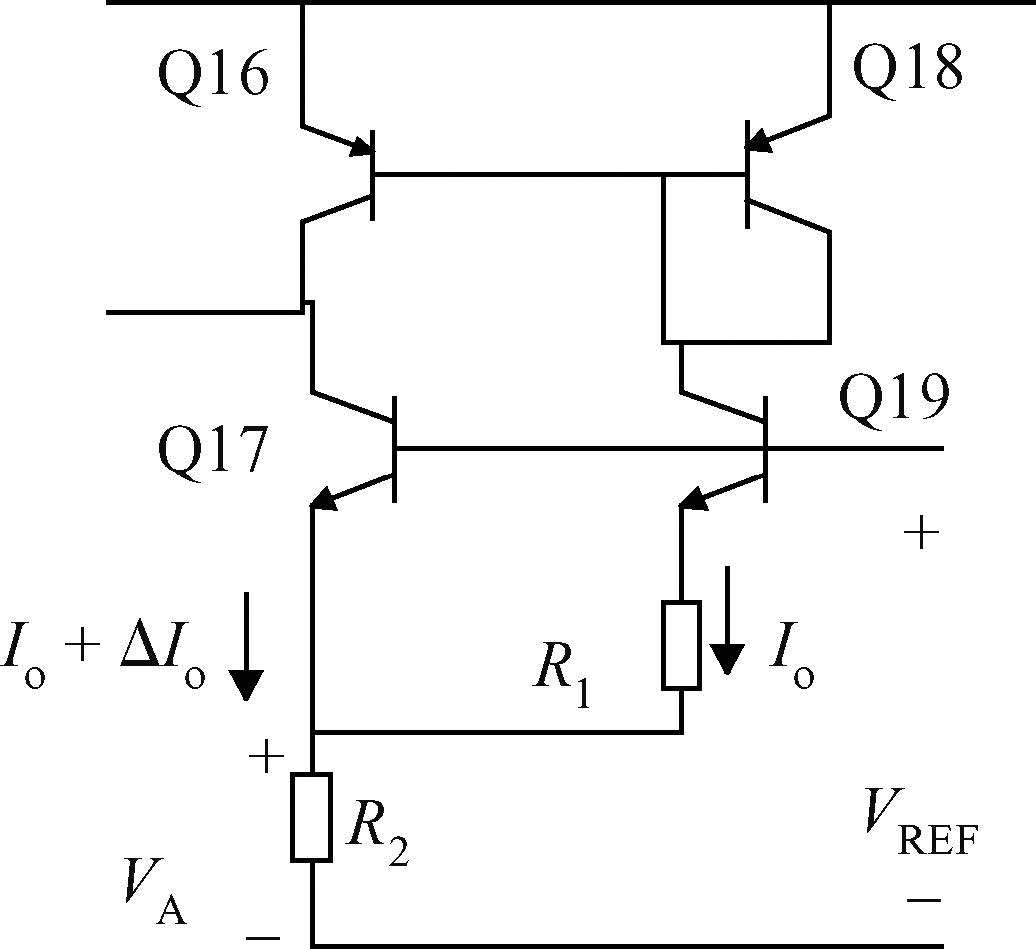
The LM117 is an adjustable 3-terminal positive voltage regulator. Figure 1 shows a circuit diagram of the LM117. The basic operation of the LM117 is described in Reference [11]. Reference [5] has identified that the degradation of the output voltage of the LM117 is decided by the degradation of the band-gap reference. The band-gap reference, shown in Figure 2, is composed of two vertical NPN bipolar junction transistors (Q17 and Q19), two lateral PNP bipolar junction transistors (Q16 and Q18), and two resistors (R1 and R2)[5].

 DownLoad:

The reference voltage, VREF, is set by:
|
VREF=VBE17+VA, |
(1) |
|
VA=R2(2Io+ΔIo). |
(2) |
The current ΔIo is zero when the base currents in all four band-gap reference transistors are neglected [5].
Combining Equations (1) and (2) gives:
|
R2(2Lo+ΔIo)=VREF−VBE17, |
(3) |
|
Io=VREF−VBE172R2−ΔIo2. |
(4) |
The two NPN bipolar junction transistors of the band-gap circuit operate at different current densities, hence different base-emitter voltages[5]. For the LM117, the current density of Q19 is 10 times the density of Q17[5],
|
Is19=10Is17, |
(5) |
|
Ic=Isexp(VBE/VT), |
(6) |
|
ΔVBE=VBE17−VBE19=VT[ln(10Ic17/Ic19)]. |
(7) |
By observing the reference circuit, one can determine that:
|
ΔVBE=R1Io. |
(8) |
Combining Equations (4) and (7) gives:
|
VREF=VBE17+2R2ΔVBE/R1+R2ΔI0. |
(9) |
Equation (9) is critical to the regulator's operation and is useful in understanding radiation-induced degradation of the output voltage.
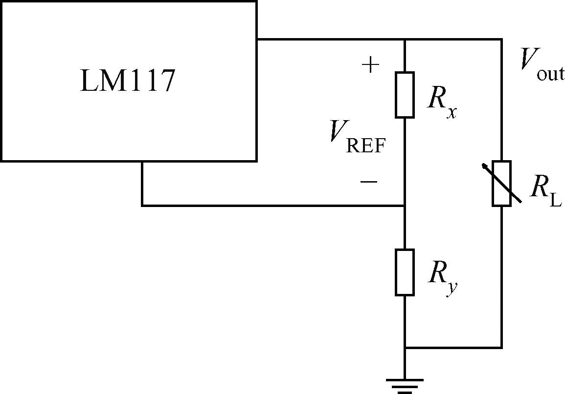
The three-terminal voltage regulator circuit shown in Figure 3 is often applied, which is also used for electrical parameter and noise parameter measurements. From Figure 3, we can obtain
|
Vout=VREFRx+RyRx, |
(10) |

2.2 Output 1/f noise voltage
Since the degradation of the LM117 is mainly caused by the degradation of the band-gap reference, and the band-gap reference is the dominant source of noise in the voltage regulators [12], the 1/f noise degradation of the band-gap reference is only considered. As shown in Figure 2, the band-gap reference is composed of two NPN transistors and PNP transistors. The radiation induces the degradation of the base surface current of the bipolar junction transistor, which leads to a degradation of base current. The changes of base current will cause the changes of the base 1/f noise of the bipolar junction transistor.
The base current IB is decomposed into a volume, IV, and surface, IS, recombination components IB=IV+IS. And the base current fluctuations are decomposed into surface and volume originated noise sources$^{ [13]. The surface noise is ascribed to the low frequency fluctuations in the surface recombination current component due to the dynamic trapping-detrapping of carriers into oxide-trapped charges. The volume noise component results from the intrinsic fluctuations of the diffusion current due to the carrier number fluctuations in the volume of the space charge region. If one assumes uncorrelated fluctuation sources both in the volume and in the surface current components, the base current 1/f noise SIB can be expressed in the form[13],
|
SIB=KSI2Sf+KVI2Vf, |
(11) |
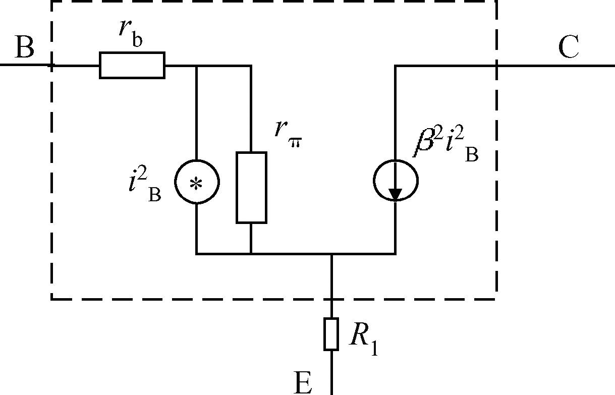
Now we only consider the bipolar transistor Q19, and assume that Q19 is a bipolar transistor without other circuits. As shown in Figure 4, the 1/f noise voltage across the B-E terminal can be given by
|
SVBE=r2b19SIB19+r2π19SIB19+R21SIB19, |
(12) |

If the base 1/f noise currents of transistors Q16 and Q18 are considered, the base 1/f noise current of Q16, SIB16, the base 1/f noise currents of Q18, SIB18, and the 1/f noise current through the collector β218SIB18 which is an amplified SIB18 would flow through the emitter of Q19. So the 1/f noise voltage across R1 would become R21[(β218+1)SIB18+SIB16]. The 1/f noise voltage across the B-E terminal can be rewritten as
|
SV1=r2bSIB19+r2πSIB19+R21SIB19+R21[(β218+1)SIB18+SIB16]. |
(13) |
Similarly, we can obtain 1/f noise voltage across R2
|
SV2=R22β216SIB16+R22(β17+1)2SIB17+R22(β19+1)2SIB19+R22[(β18+1)2SIB18+SIB16]. |
(14) |
From Figure 2, we can obtain
|
SVREF=SV1+SV2. |
(15) |
According to Figure 3, we can obtain 1/f noise voltage at the output terminal
|
SV=SVREF(Rx+RyRx)2. |
(16) |
If we assume that the 1/f noise voltage in the other noise source is SVother, we can obtain the total output 1/f noise voltage
|
SVout=SVREF(Rx+RyRx)2+SVother. |
(17) |
3. Experiment and discussion
3.1 Experiment
The LM117 adjustable 3-terminal positive voltage regulators were used in this work. All regulators were irradiated with ionizing gamma-radiation from a Co60 source at room temperature. The dose rate was 0.1 Gy(Si)/s. The accumulated total dose at each test step was 100, 300, 500, 700 Gy(Si). The devices were periodically removed from the source in order to track the changes in the device parameters at each total dose level. The output voltage was set 10 V by configuring the proper resistance (Rx and Ry). The output current was set to 20 mA by configuring the proper resistance RL. The bias conditions were held constant during the radiation and the measurement. The measured electrical parameter was the output voltage, which was measured using a multimeter. The measured noise parameter was the output noise voltage SVout, which was measured with the XD3020 noise measurement system that was described in Reference [14]. The circuit was used for parameter measurements, as shown in Figure 3.
3.2 Result and discussion
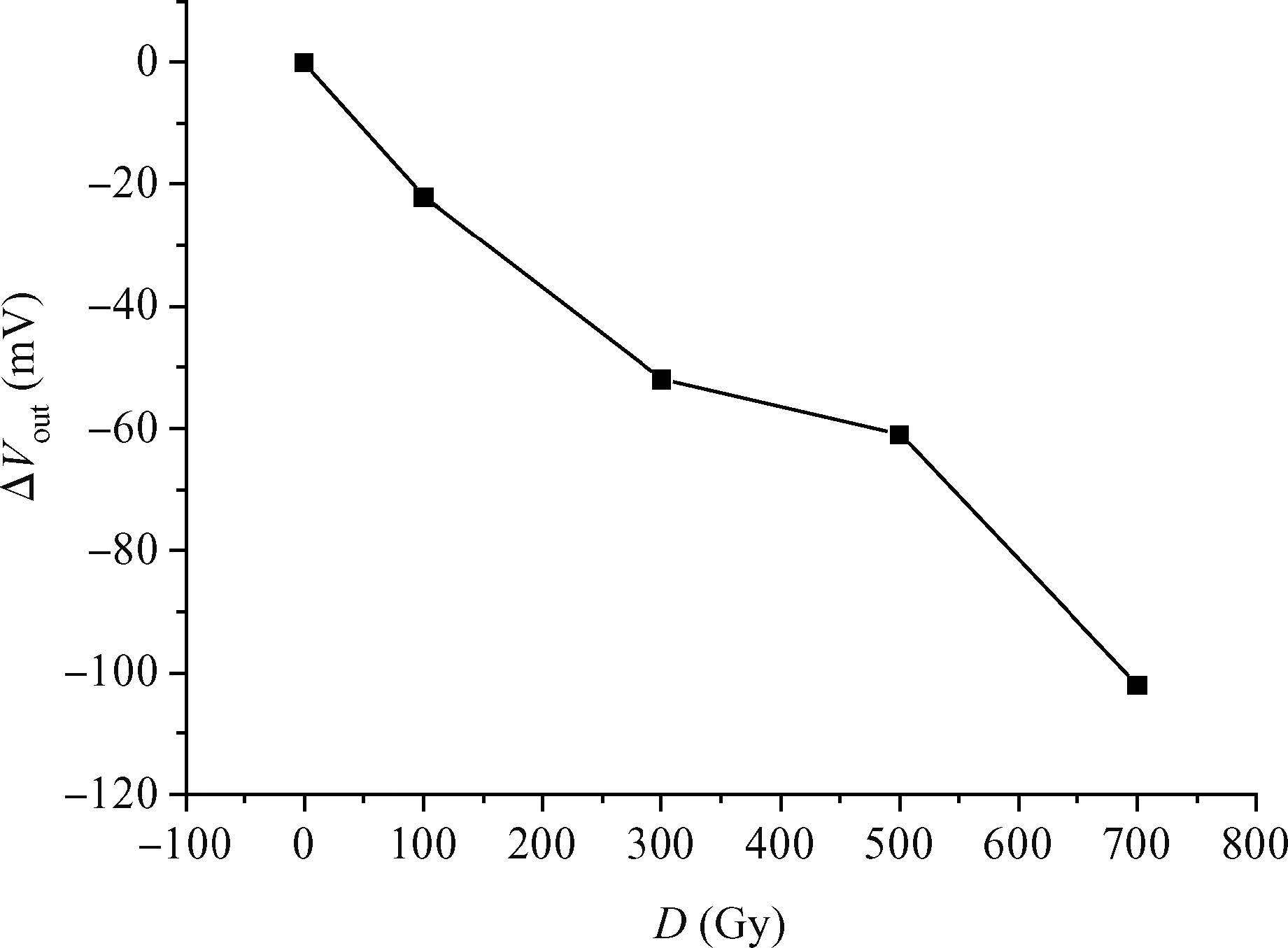
The variance in the output voltage, ΔVout, is plotted versus the total dose in Figure 5, where ΔVout=Vout−Vout0, Vout0 are the pre-irradiation parameters, and Vout0 is post-irradiation parameter. The output voltage decreased with the increase in the total dose. According to Equation (10), the variation of output voltage was caused by the reference voltage. Many studies show that radiation-induced current gain degradations in NPN and PNP bipolar junction transistors are due to the accumulation of oxide-trapped charges and interface states at the surface of the device[15, 16, 17, 18]. The band-gap reference is composed of two NPN transistors and two PNP transistors. First, we consider the change in the PNP transistor, and assume no change in the NPN transistor. When the radiation leads to an increase in the base current of the PNP transistor, this causes the collector current of Q17 to drop relative to the collector current in Q19. According to Equation (7), ΔVBE drops , and ΔIo becomes negative. According to Equation (9), this causes the reference voltage to drop. Then, we consider the change in the NPN transistor and assume no change in the PNP transistor. When the radiation leads to an increase in the base current of the NPN transistor, since the collector currents of Q19 and Q17 remain unchanged, ΔVBE will not change. Prior to the radiation, the base currents of both transistors are matched. However, as the part was exposed to more total dose, the base current of Q19 will change significantly more than the base current of Q17. This is because Ql9 operates at a base to emitter voltage which is 60 mV less than that of Q17[5]. This makes ΔIo become negative. According to Equation (9), this causes the reference voltage to drop. So, radiation-induced current degradations in the NPN and PNP transistors would reduce the reference voltage. According to Equation (10), the output voltage would drop.

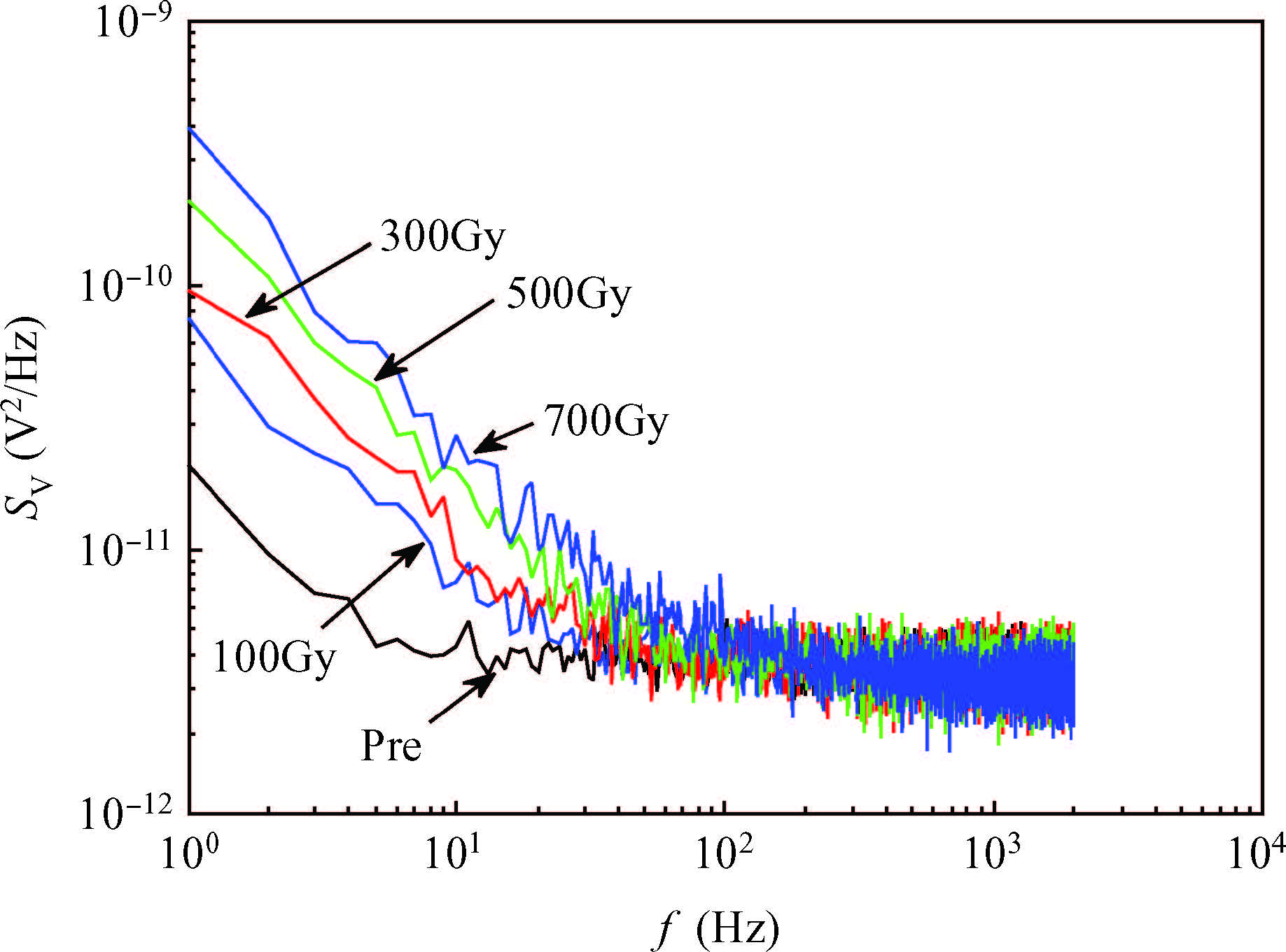
The noise performance with the accumulated total dose is shown in Figure 6. Figure 6 shows that low frequency 1/f noise increases with the total dose.

The power spectral density of the voltage can be commonly expressed as follows:
|
SV=A+B/fγ, |
(18) |
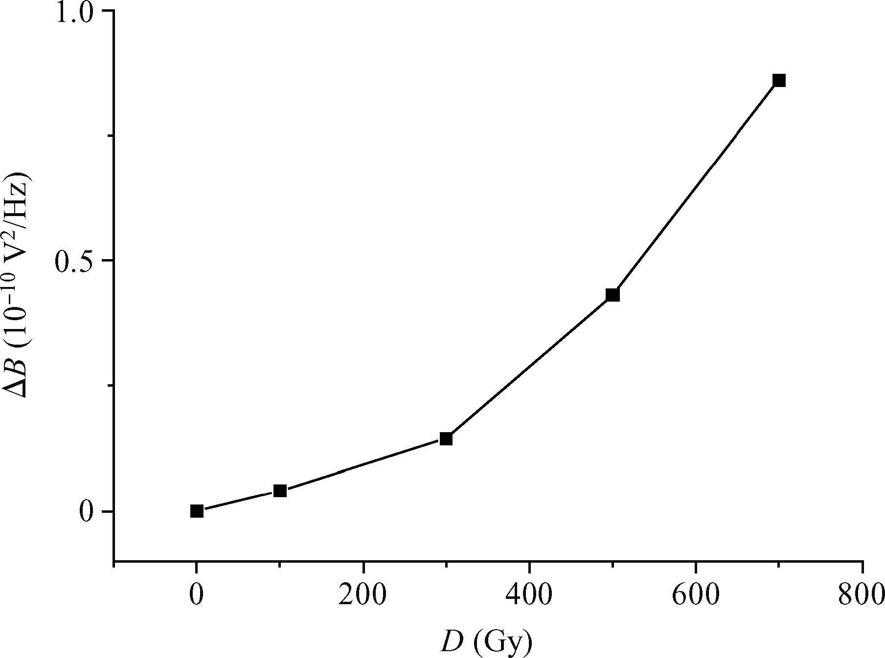
At the frequency range of 10-100 Hz, the graph of ΔB as a function of the doses is shown in Figure 7, where ΔB=B−B, B0 and B are the pre-irradiation and post-irradiation amplitude of 1/f noise, respectively. As shown in Figure 7, ΔB increase with the dose.

Since the band-gap reference is the dominant noise source, and its degradation causes the variation of the output voltage, we only consider the variation of the 1/f noise voltage of the band-gap reference, and assume that it leads to the variation of the output 1/f noise voltage. According to Equation (17), we can obtain the following relationship
|
ΔSVout=ΔSVREF(Rx+RyRx)2. |
(19) |
According to Equation (11), the base surface 1/f noise current increases with the base surface current, which leads to an increase in the base 1/f noise current. When the transistor is in the forward active region, β≫1. From Equations (13), (14), and (15), we can obtain the following relationship:
|
SVREF=r2bSIB19+r2πSIB19+R21SIB19+R21(β218SIB18+SIB16)+R22β216SIB16+R22β217SIB17+R22β219SIB19+R22(β218SIB18+SIB16). |
(20) |
Similarly, first, we consider the change in the PNP transistor, and assume no change in the NPN transistor. The radiation leads to an increase in the base current of the PNP transistor, which leads to a reduction in the current gain. For 1/f noise voltage, we need to determine the change of R22β216SIB16. R22β216SIB16 can be written as
|
β216SIB16=KS(ICIV+IS)2I2Sf=(ICIV/IS+1)2KSf. |
(21) |
From Equation (21), we can see that the current gain β=IC/(IV/IS+1) increases with the base surface current IS, which makes β216SIB16 increase. So R21[β218SIB18+SIB16]+R22β216SIB16+R22(β218SIB18+SIB16) increases. According to Equations (19) and (20), the output 1/f noise voltage increases. Similarly, the radiation leads to an increase in the base current of NPN transistors, which will lead to an increase in the output 1/f noise voltage. So we can draw a conclusion that the output 1/f noise voltage increases with the total dose.
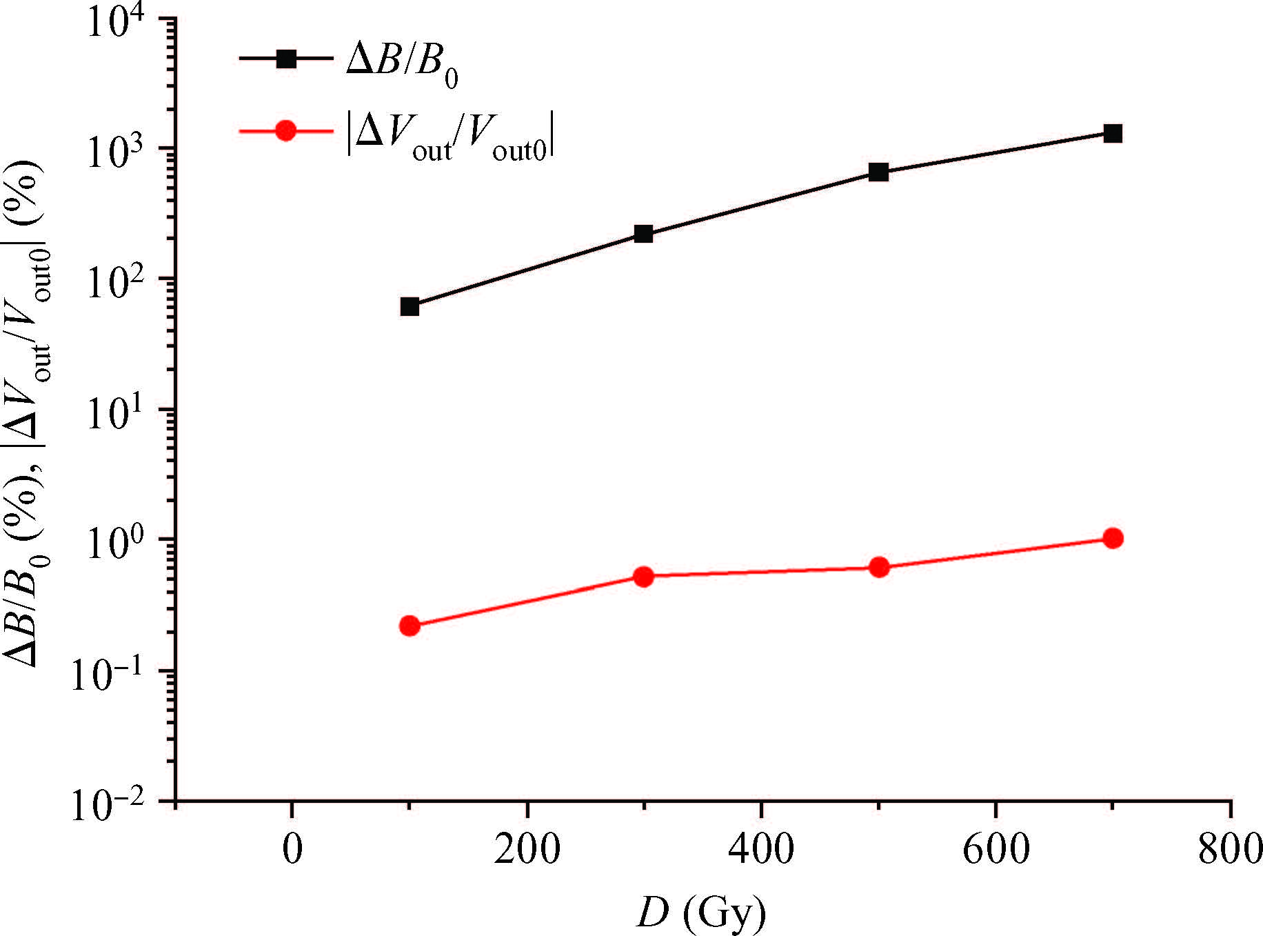
The output voltage and the output 1/f noise voltage degradation of LM117 can be attributed to the same physical origin, and these two kinds of degradations are the results of the degradation of the band-gap reference. So the output 1/f noise voltage may be used as a means to evaluate the radiation resistance capability of LM117. In order to make a comparison, ΔB/B0 and |ΔVout/Vout0| are plotted versus the total dose in Figure 8. Notice that this is a semi-log graph. Figure 8 shows that their degradations have a similar trend, and the increase in the output 1/f noise voltage is more significant than in the output voltage on the same total dose. After a radiation dose up to 700 Gy(Si), |ΔVout/Vout0| is 1%, and ΔB/B0 is 1305%. It is clear that the ΔB/B0 is more sensitive than |ΔVout/Vout0|.

4. Conclusion
The radiations cause the variance of the output voltage and 1/f noise voltage. These two kinds of degradations are caused by the degradation in the band-gap reference. The radiations cause an increase in the base surface current of NPN and PNP bipolar junction transistors of the band-gap reference, which leads to the degradation in the output voltage. At the same time, the 1/f noise of the band-gap reference increases with the increase in the base surface current of bipolar junction transistors, which brings about an increase in the output 1/f noise voltage. Compared to the electrical parameter, the 1/f noise parameter is more sensitive. In this work, 30 devices were radiated. Although the number of samples is small, on the basis of the research, 1/f noise measurement may be used as a means to evaluate the radiation resistance capability of LM117. Also, 1/f noise has been already used to evaluate the radiation resistance capability of many devices, for example, the MOS transistor[19, 20] and optoelectronic coupled devices[21]. In theory, 1/f noise may be used as a means to evaluate the radiation resistance capability of other devices. Continuing to study the 1/f noise of other devices will be the future works.

 DownLoad:


 DownLoad:


