| [1] |
Agafonov O B, Dais C, Grützmacher D, et al. Quantum confinement effects in Si/Ge heterostructures with spatially ordered arrays of self-assembled quantum dots. Appl Phys Lett, 2010, 96(22): 222107 doi: 10.1063/1.3442508 |
| [2] |
Wang K L. Ge/Si self-assembled quantum dots and their optoelectronic device applications. Proc IEEE, 2007, 95(9): 1866 doi: 10.1109/JPROC.2007.900971 |
| [3] |
Zhang J J, Katsaros G, Montalenti F, et al. Monolithic growth of ultrathin Ge nanowires on Si (001). Phys Rev Lett, 2012, 109(8): 085502 doi: 10.1103/PhysRevLett.109.085502 |
| [4] |
Katsaros G, Spathis P, Stoffel M, et al. Hybrid superconductor-semiconductor devices made from self-assembled SiGe nanocrystals on silicon. Nat Nanotech, 2010, 5(6): 458 doi: 10.1038/nnano.2010.84 |
| [5] |
Xia J S, Ikegami Y, Shiraki Y, et al. Strong resonant luminescence from Ge quantum dots in photonic crystal microcavity at room temperature. Appl Phys Lett, 2006, 89(20): 201102 doi: 10.1063/1.2386915 |
| [6] |
Xia J S, Nemoto K, Ikegami Y, et al. Silicon-based light emitters fabricated by embedding Ge self-assembled quantum dots in microdisks. Appl Phys Lett, 2007, 91(1): 011104 doi: 10.1063/1.2754356 |
| [7] |
Hrauda N, Zhang J, Wintersberge E, et al. X-ray nanodiffraction on a single SiGe quantum dot inside a functioning field-effect transistor. Nano Lett, 2011, 11(7): 2875 doi: 10.1021/nl2013289 |
| [8] |
Sánchez-Péreza J R, Boztug C, Chen F, et al. Direct-bandgap light-emitting germanium in tensilely strained nanomembranes. PNAS, 2011, 108(47): 18893 doi: 10.1073/pnas.1107968108 |
| [9] |
Arapkina L V, Yuryev V A. Atomic structure of Ge quantum dots on the Si (001) Surface. JETP Lett, 2010, 91(6): 281 doi: 10.1134/S0021364010060056 |
| [10] |
Capellini G, De Seta M, Di Gaspare L, et al. Evolution of Ge/Si (001) islands during Si capping at high temperature. J Appl Phys, 2005, 98(12): 124901 doi: 10.1063/1.2141652 |
| [11] |
McKay M R, Venables J A, Drucker J. Kinetically suppressed ostwald ripening of Ge/Si (100) hut clusters. Phys Rev Lett, 2008, 101(21): 216104 doi: 10.1103/PhysRevLett.101.216104 |
| [12] |
Richard M I, Schülli T U, Renaud G, et al. In situ X-ray scattering study on the evolution of Ge island morphology and relaxation for low growth rate: advanced transition to superdomes. Phys Rev B, 2009, 80(4): 045313 doi: 10.1103/PhysRevB.80.045313 |
| [13] |
Alonso M I, de la Calle M, Ossó J O, et al. Strain and composition profiles of self-assembled Ge/Si (001) islands. J Appl Phys, 2005, 98(3): 033530 doi: 10.1063/1.2006229 |
| [14] |
Koguchi N, Ishige K. Growth of GaAs epitaxial microcrystals on an S-terminated GaAs substrate by successive irradiation of Ga and As molecular beams. Jpn J Appl Phys I, 1993, 32(5A): 2052
|
| [15] |
Yang B, Liu F, Lagally M G. Local strain-mediated chemical potential control of quantum dot self-organization in heteroepitaxy. Phys Rev Lett, 2004, 92(2): 025502 doi: 10.1103/PhysRevLett.92.025502 |
| [16] |
Persichetti L, Sgarlata A, Fanfoni M, et al. Ripple-to-dome transition: the growth evolution of Ge on vicinal Si (1110) surface. Phys Rev B, 2010, 82(12): 121309 doi: 10.1103/PhysRevB.82.121309 |
| [17] |
Nie T X, Lin J H, Chen Z G, et al. Thermally oxidized formation of new Ge dots over as-grown Ge dots in the Si capping layer. J Appl Phys, 2011, 110(11): 114304 doi: 10.1063/1.3665398 |
| [18] |
Zhong Z, Schwinger W, Schäffler F, et al. Delayed plastic relaxation on patterned Si substrates: Coherent SiGe pyramids with dominant {111} facets. Phys Rev Lett, 2007, 98(17): 176102 doi: 10.1103/PhysRevLett.98.176102 |
| [19] |
Ma Y, Cui J, Fan Y, et al. Ordered GeSi nanorings grown on patterned Si (001) substrates. Nanoscale Res Lett, 2011, 6: 205 doi: 10.1186/1556-276X-6-205 |
| [20] |
Zhou T, Zhong Z. Dramatically enhanced self-assembly of GeSi quantum dots with superior photoluminescence induced by the substrate misorientation. APL Mater, 2014, 2(2): 022108 doi: 10.1063/1.4866356 |
| [21] |
Beirne G J, Hermannstadter C, Wang L, et al. Quantum light emission of two lateral tunnel-coupled (In,Ga)As/GaAs quantum dots controlled by a tunable static electric field. Phys Rev Lett, 2006, 96(13): 137401 doi: 10.1103/PhysRevLett.96.137401 |
| [22] |
Grützmacher D, Fromherz T, Dais C, et al. Three-dimensional Si/Ge quantum dot crystals. Nano Lett, 2007, 7(10): 3150 doi: 10.1021/nl0717199 |
| [23] |
Hu H, Gao H J, Liu F. Theory of directed nucleation of strained islands on patterned substrates. Phys Rev Lett, 2008, 101(21): 216102 doi: 10.1103/PhysRevLett.101.216102 |
| [24] |
Zhong Z Y, Chen P X, Jiang Z M, et al. Temperature dependence of ordered GeSi island growth on patterned Si (001) substrates. Appl Phys Lett, 2008, 93(4): 043106 doi: 10.1063/1.2965484 |
| [25] |
Bollani M, Chrastina D, Fedorov A, et al. Ge-rich islands grown on patterned Si substrates by low-energy plasma-enhanced chemical vapour deposition. Nanotechnology, 2010, 21(47): 475302 doi: 10.1088/0957-4484/21/47/475302 |
| [26] |
Zhong Z Y, Halilovic A, Mühlberger M, et al. Positioning of self-assembled Ge islands on stripe-patterned Si (001) substrates. J Appl Phys, 2003, 93(10): 6258 doi: 10.1063/1.1566455 |
| [27] |
|
| [28] |
Qin X R, Swartzentruber B S, Lagally M G. Diffusional kinetics of SiGe dimers on Si (100) using atom-tracking scanning tunneling microscopy. Phys Rev Lett, 2000, 85(17): 3660 doi: 10.1103/PhysRevLett.85.3660 |
| [29] |
Zhong Z, Bauer G. Site-controlled and size-homogeneous Ge islands on prepatterned Si (001) substrates. Appl Phys Lett, 2004, 84(11): 1922 doi: 10.1063/1.1664014 |
| [30] |
Boioli F, Gatti R, Grydlik M, et al. Assessing the delay of plastic relaxation onset in SiGe islands grown on pit-patterned Si (001) substrates. Appl Phys Lett, 2011, 99(3): 033106 doi: 10.1063/1.3615285 |
| [31] |
Jin G, Liu J L, Thomas S G, et al. Controlled arrangement of self-organized Ge islands on patterned Si (001) substrates. Appl Phys Lett, 1999, 75(18): 2752 doi: 10.1063/1.125138 |
| [32] |
Chen H M, Kuan C H, Suen Y W, et al. Thermally induced morphology evolution of pit-patterned Si substrate and its effect on nucleation properties of Ge dots. Nanotechnology, 2012, 23(1): 015303 doi: 10.1088/0957-4484/23/1/015303 |
| [33] |
Katsaros G, Tersoff J, Stoffel M, et al. Positioning of strained islands by interaction with surface nanogrooves. Phys Rev Lett, 2008, 101(9): 096103 doi: 10.1103/PhysRevLett.101.096103 |
| [34] |
Chen Y R, Kuan C H, Suen Y W, et al. High-density one-dimensional well-aligned germanium quantum dots on a nanoridge array. Appl Phys Lett, 2008, 93(8): 083101 doi: 10.1063/1.2976549 |
| [35] |
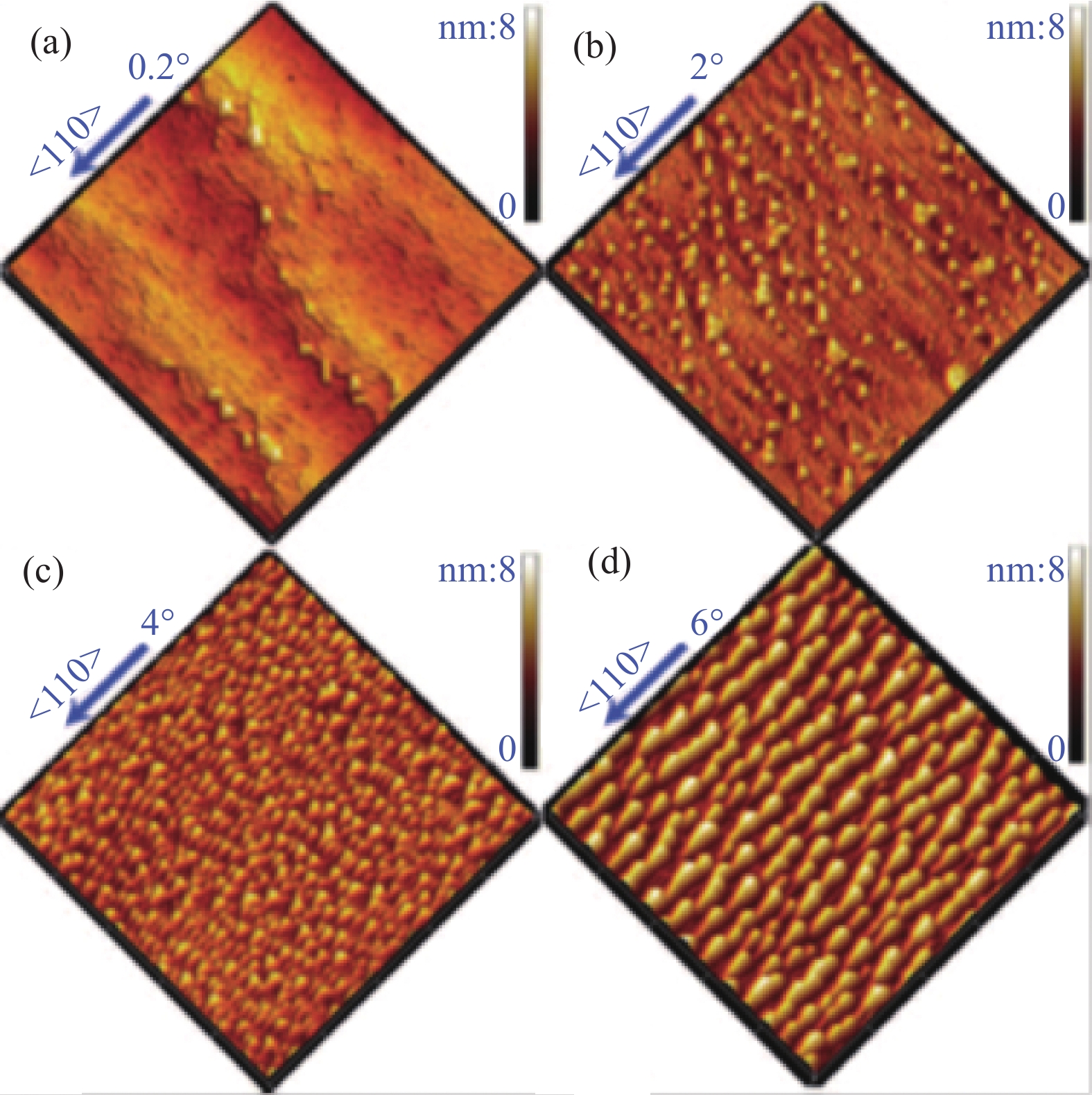
Olzierski A, Nassiopoulou A G, Raptis I, et al. Two-dimensional arrays of nanometre scale holes and nano-V-grooves in oxidized Si wafers for the selective growth of Ge dots or Ge/Si hetero-nanocrystals. Nanotechnology, 2004, 15(11): 1695 doi: 10.1088/0957-4484/15/11/056 |
| [36] |
Zhong Z, Schmidt O G, Bauer G, et al. Increase of island density via formation of secondary ordered islands on pit-patterned Si (001) substrates. Appl Phys Lett, 2005, 87(13): 133111 doi: 10.1063/1.2061870 |
| [37] |
Zhong Z, Bauer G. Site-controlled and size-homogeneous Ge islands on prepatterned Si (001) substrates. Appl Phys Lett, 2004, 84(11): 1922 doi: 10.1063/1.1664014 |
| [38] |
Zhang J J, Rastelli A, Schmidt O G, et al. Compositional evolution of SiGe islands on patterned Si (001) substrates. Appl Phys Lett, 2010, 97(20): 203103 doi: 10.1063/1.3514239 |
| [39] |
Hackl F, Grydlik M, Brehm M, et al. Microphotoluminescence and perfect ordering of SiGe islands on pit-patterned Si (001) substrates. Nanotechnology, 2011, 22(16): 165302 doi: 10.1088/0957-4484/22/16/165302 |
| [40] |
Lausecker E, Brehm M, Grydlik M, et al. UV nanoimprint lithography for the realization of large-area ordered SiGe/Si (001) island arrays. Appl Phys Lett, 2011, 98(14): 143101 doi: 10.1063/1.3575554 |
| [41] |
Ma Y J, Zeng C, Zhou T, et al. Ordering of low-density Ge quantum dot on patterned Si substrate. J Phys D, 2014, 47(48): 485303 doi: 10.1088/0022-3727/47/48/485303 |
| [42] |
Lei H, Zhou T, Wang S G, et al. Large-area ordered Ge–Si compound quantum dot molecules on dot-patterned Si (001) substrates. Nanotechnology, 2014, 25(34): 345301 doi: 10.1088/0957-4484/25/34/345301 |
| [43] |
Zhong Z, Halilovic A, Fromherz T, et al. Two-dimensional periodic positioning of self-assembled Ge islands on prepatterned Si (001) substrates. Appl Phys Lett, 2003, 82(26): 4779 doi: 10.1063/1.1581986 |
| [44] |
Chen P X, Fan Y L, Zhong Z Y. The fabrication and application of patterned Si (001) substrates with ordered pits via nanosphere lithography. Nanotechnology, 2009, 20(9): 095303 doi: 10.1088/0957-4484/20/9/095303 |
| [45] |
Baumann V, Stumpf F, Steinl T, et al. Site-controlled growth of InP/GaInP quantum dots on GaAs substrates. Nanotechnology, 2012, 23(37): 375301 doi: 10.1088/0957-4484/23/37/375301 |
| [46] |
Kiravittaya S, Rastelli A, Schmidt O G. Self-assembled InAs quantum dots on patterned GaAs (001) substrates: Formation and shape evolution. Appl Phys Lett, 2005, 87(24): 243112 doi: 10.1063/1.2143125 |
| [47] |
Chen Y W, Pan B Y, Nie T X, et al. Enhanced photoluminescence dut to lateral ordering of GeSi quantum dots on patteren Si (001) substrates. Nanotechnology, 2010, 21(17): 175701 doi: 10.1088/0957-4484/21/17/175701 |
| [48] |
Sugaya T, Amano T, Mori M, et al. Miniband formation in InGaAs quantum dot superlattice. Appl Phys Lett, 2010, 97(4): 043112 doi: 10.1063/1.3470108 |
| [49] |
Rodriguez-Bolivar S, Gomez-Campos F M, Luque-Rodriguez A, et al. Miniband structure and photon absorption in regimented quantum dot systems. J Appl Phys, 2011, 109(7): 074303 doi: 10.1063/1.3562160 |
| [50] |
Lazarenkova O L, Balandin A A. Electron and phonon energy spectra in a three-dimensional regimented quantum dot superlattice. Phys Rev B, 2002, 66(24): 245319 doi: 10.1103/PhysRevB.66.245319 |
| [51] |
Shao Q, Balandin A A, Fedoseyev A I, et al. Intermediate-band solar cells based on quantum dot supracrystals. Appl Phys Lett, 2007, 91(16): 163503 doi: 10.1063/1.2799172 |
| [52] |
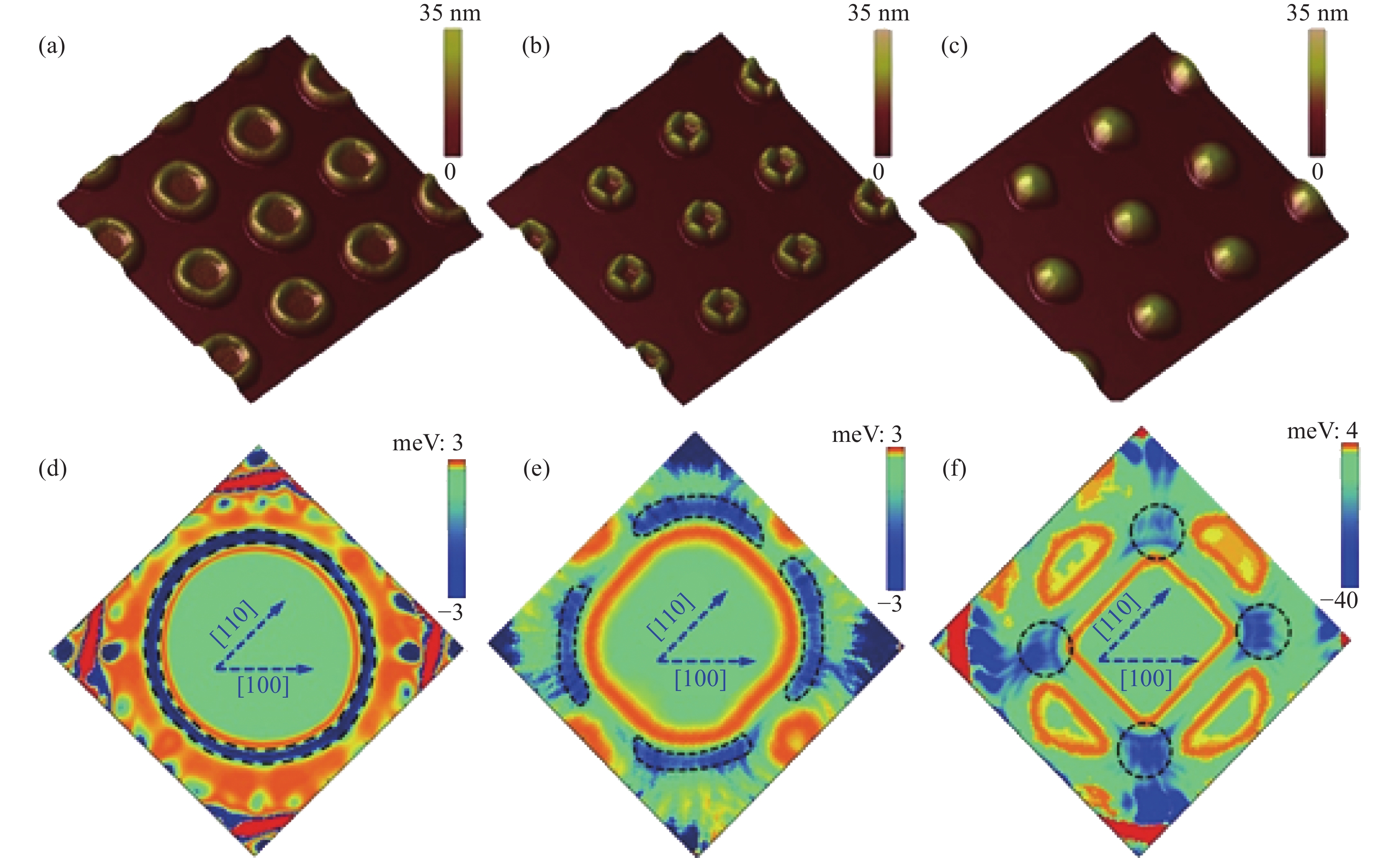
Ma Y J, Zhong Z, Lv Q, et al. Formation of coupled three-dimensional GeSi quantum dot crystals. Appl Phys Lett, 2012, 100(15): 153113 doi: 10.1063/1.3702883 |
| [53] |
Ma Y J, Zhong Z Y, Yang X J, et al. Factors influencing epitaxial growth of three-dimensional Ge quantum dot crystals on pit-patterned Si substrate. Nanotechnology, 2013, 24(1): 015304 doi: 10.1088/0957-4484/24/1/015304 |
| [54] |
Ma Y J, Zhong Z Y, Lv Q, et al. Optical properties of coupled three-dimensional Ge quantum dot crystals. Opt Express, 2013, 21(5): 6053 doi: 10.1364/OE.21.006053 |
| [55] |
Cui J, He Q, Jiang X. Self-assembled SiGe quantum rings grown on Si (001) by molecular beam epitaxy. Appl Phys Lett, 2003, 83(14): 2907 doi: 10.1063/1.1616992 |
| [56] |
Cui J, Lv Y, Yang X J, et al. Influencing factors on the size uniformity of self-assembled SiGe quantum rings grown by molecular beam epitaxy. Nanotechnology, 2011, 22: 125601 doi: 10.1088/0957-4484/22/12/125601 |
| [57] |
Lei H, Zhou T, Wang S G, et al. Large-area ordered Ge–Si compound quantum dot molecules on dot-patterned Si (001) substrates. Nanotechnology, 2014, 25(34): 345301 doi: 10.1088/0957-4484/25/34/345301 |
| [58] |
Hsieh C Y, Shim Y P, Korkusinski M. Physics of lateral triple quantum-dot molecules with controlled electron numbers. Rep Prog Phys, 2012, 75(11): 114501 doi: 10.1088/0034-4885/75/11/114501 |
| [59] |
Doty M F, Scheibner M, Ponomarev I V, et al. Electrically tunable g factors in quantum dot molecular spin states. Phys Rev Lett, 2006, 97(19): 197202 doi: 10.1103/PhysRevLett.97.197202 |
| [60] |
Doty M F, Climente J I, Korkusinski M. Antibonding ground states in InAs quantum-dot molecules. Phys Rev Lett, 2009, 102(4): 047401 doi: 10.1103/PhysRevLett.102.047401 |
| [61] |
Doty M F, Climente J I, Greilich A, et al. Hole-spin mixing in InAs quantum dot molecules. Phys Rev B, 2010, 81(3): 035308 doi: 10.1103/PhysRevB.81.035308 |
| [62] |
Boyer de la Giroday A, Sköld N, Stevenson R M, et al. Exciton-spin memory with a semiconductor quantum dot molecule. Phys Rev Lett, 2011, 106(21): 216802 doi: 10.1103/PhysRevLett.106.216802 |
| [63] |
Shtrichman I, Metzner C, Gerardot B D, et al. Photoluminescence of a single InAs quantum dot molecule under applied electric field. Phys Rev B, 2002, 65(8): 081303 doi: 10.1103/PhysRevB.65.081303 |
| [64] |
Lei K W, West T, Zhu X Y. Template-assembly of quantum dot molecules. J Phys Chem B, 2013, 117(16): 4582 doi: 10.1021/jp308706b |
| [65] |
Overgaag K, Liljeroth P, Grandidier B, et al. Scanning tunneling spectroscopy of individual PbSe quantum dots and molecular aggregates stabilized in an inert nanocrystal matrix. ACS Nano, 2008, 2(3): 600 doi: 10.1021/nn7003876 |
| [66] |
Vandervelde T E, Kumar P, Kobayashi T, et al. Growth of quantum fortress structures in Si 1-xGe x/Si via combinatorial deposition. Appl Phys Lett, 2003, 83(25): 5205 doi: 10.1063/1.1636268 |
| [67] |
Gray J L, Singh N, Elzey D M, et al. Kinetic size selection mechanisms in heteroepitaxial quantum dot molecules. Phys Rev Lett, 2004, 92(13): 135504 doi: 10.1103/PhysRevLett.92.135504 |
| [68] |
Gray J L, Hull R, Floro J A. Control of surface morphology through variation of growth rate in SiGe/Si (100) epitaxial films: nucleation of " quantum fortresses”. Appl Phys Lett, 2002, 81(13): 2445 doi: 10.1063/1.1509094 |
| [69] |
Ma Y J, Huang F S, Zeng C, et al. Towards controllable growth of self-assembled SiGe single and double quantum dot nanostructures. Nanoscale, 2014, 6(8): 3941 doi: 10.1039/C3NR04114J |
| [70] |
Persichetti L, Sgarlata A, Fanfoni M, et al. Shaping Ge islands on Si (001) surfaces with misorientation angle. Phys Rev Lett, 2010, 104(3): 036104 doi: 10.1103/PhysRevLett.104.036104 |
| [71] |
Spencer B J, Tersoff J. Asymmetry and shape transitions of epitaxially strained islands on vicinal surfaces. Appl Phys Lett, 2010, 96(7): 073114 doi: 10.1063/1.3318256 |
| [72] |
Chen G, Sanduijav B, Matei D, et al. Formation of Ge nanoripples on vicinal Si (1110): from Stranski-Krastanow seeds to a perfectly faceted wetting layer. Phys Rev Lett, 2012, 108(5): 055503 doi: 10.1103/PhysRevLett.108.055503 |
| [73] |
Persichetti L, Sgarlata A, Fanfoni M, et al. Breaking elastic field symmetry with substrate vicinality. Phys Rev Lett, 2011, 106(5): 055503 doi: 10.1103/PhysRevLett.106.055503 |
| [74] |
Sanduijav B, Scopece D, Matei D, et al. One-dimensional to three-dimensional ripple-to-dome transition for SiGe on vicinal Si (1110). Phys Rev Lett, 2012, 109(2): 025505 doi: 10.1103/PhysRevLett.109.025505 |
| [75] |
Pan J, Zhou T, Jiang Z. Anomalous magnetoresistance of an array of GeSi nanowires. Appl Phys Lett, 2013, 102(18): 183108 doi: 10.1063/1.4804295 |
| [76] |
Gong H, Chen P X, Ma Y J, et al. Formation and characterization of multilayer GeSi nanowires on miscut Si (001) substrates. J Nanosci Nanotechnol, 2013, 13(2): 834 doi: 10.1166/jnn.2013.5979 |
| [77] |
Zhou T, Zhong Z Y. Unique features of laterally aligned GeSi nanowires self-assembled on the vicinal Si (001) surface misoriented toward the [100] direction. Nanoscale, 2015, 7(13): 5835 doi: 10.1039/C4NR07433E |
| [78] |
Zhou T, Zeng C, Ma Q Q, et al. Controlled formation of GeSi nanostructures on periodic Si (001) sub-micro pillars. Nanoscale, 2014, 6(8): 3925 doi: 10.1039/C3NR04146H |
| [79] |
Wang S G, Zhou T, Li D J, et al. Evolution and engineering of precisely controlled Ge nanostructures on scalable array of ordered Si nano-pillars. Sci Rep, 2016, 6: 28872 doi: 10.1038/srep28872 |
| [80] |
Jiang Y W, Mo D L, Hu X F, et al. Investigation on Ge surface diffusion via growing Ge quantum dots on top of Si pillars. AIP Adv, 2016, 6(8): 085120 doi: 10.1063/1.4961992 |
| [81] |
Wu Z, Lei H, Zhou T, et al. Fabrication and characterization of SiGe coaxial quantum wells on ordered Si nanopillars. Nanotechnology, 2014, 25(25): 055204
|
| [82] |
Jiang Y W, Huang S F, Zhu Z C, et al. Fabrication and photoluminescence study of large-area ordered and size-controlled GeSi multi-quantum-well nanopillar arrays. Nanoscale Res Lett, 2016, 11: 102 doi: 10.1186/s11671-016-1312-1 |
| [83] |
Katsaros G, Spathis P, Stoffel M, et al. Hybrid superconductor-semiconductor devices made from self-assembled SiGe nanocrystals on silicon. Nat Nanotechnol, 2010, 5(6): 458 doi: 10.1038/nnano.2010.84 |
| [84] |
|
| [85] |
Birowosuto M D, Sumikura H, Matsuo S, et al. Fast purcell-enhanced single photon source in 1550-nm telecom band from a resonant quantum dot-cavity coupling. Sci Rep, 2012, 2: 321 doi: 10.1038/srep00321 |
| [86] |
Mohan A, Felici M, Gallo P, et al. Polarization-entangled photons produced with high-symmetry site-controlled quantum dots. Nat Photonics, 2010, 4(5): 302 doi: 10.1038/nphoton.2010.2 |
| [87] |
Nomura M, Kumagai N, Iwamoto S, et al. Laser oscillation in a strongly coupled single quantum dot-nanocavity system. Nat Phys, 2010, 6(4): 279 doi: 10.1038/nphys1518 |
| [88] |
Strauf S, Hennessy K, Rakher M T, et al. Self-tuned quantum dot gain in photonic crystal lasers. Phys Rev Lett, 2006, 96(12): 127404 doi: 10.1103/PhysRevLett.96.127404 |
| [89] |
Ellis B, Mayer M A, Shambat G. Ultralow-threshold electrically pumped quantum-dot photonic-crystal nanocavity laser. Nat Photonics, 2011, 5(5): 297 doi: 10.1038/nphoton.2011.51 |
| [90] |
Hennessy K, Badolato A, Winger M, et al. Quantum nature of a strongly coupled single quantum dot-cavity system. Nature, 2007, 445(7130): 896 doi: 10.1038/nature05586 |
| [91] |
Yoshie T, Scherer A, Hendrickson J, et al. Vacuum Rabi splitting with a single quantum dot in a photonic crystal nanocavity. Nature, 2004, 432(7014): 200 doi: 10.1038/nature03119 |
| [92] |
Xia J, Takeda Y, Usami N, et al. Room-temperature electroluminescence from Si microdisks with Ge quantum dots. Opt Express, 2010, 18(13): 13945 doi: 10.1364/OE.18.013945 |
| [93] |
Xu X, Narusawa S, Chiba T, et al. Silicon-based lightemitting devices based on Ge self-assembled quantum dots embedded in optical cavities. IEEE J Sel Top Quantum Electron, 2012, 218(6): 1830
|
| [94] |
Zhang Y, Zeng C, Li D, et al. Enhanced light emission from Ge quantum dots in photonic crystal ring resonator. Opt Express, 2014, 22(10): 12248 doi: 10.1364/OE.22.012248 |
| [95] |
Jannesari R, Schatzl M, Hackl F. Commensurate germanium light emitters in silicon-on-insulator photonic crystal slabs. Opt Express, 2014, 22(21): 25426 doi: 10.1364/OE.22.025426 |
| [96] |
Zhang Y, Zeng C, Li D, et al. Enhanced 1524-nm emission from Ge quantum dots in a modified photonic crystal L3 cavity. IEEE Photonics J, 2013, 5(5): 4500607 doi: 10.1109/JPHOT.2013.2280525 |
| [97] |
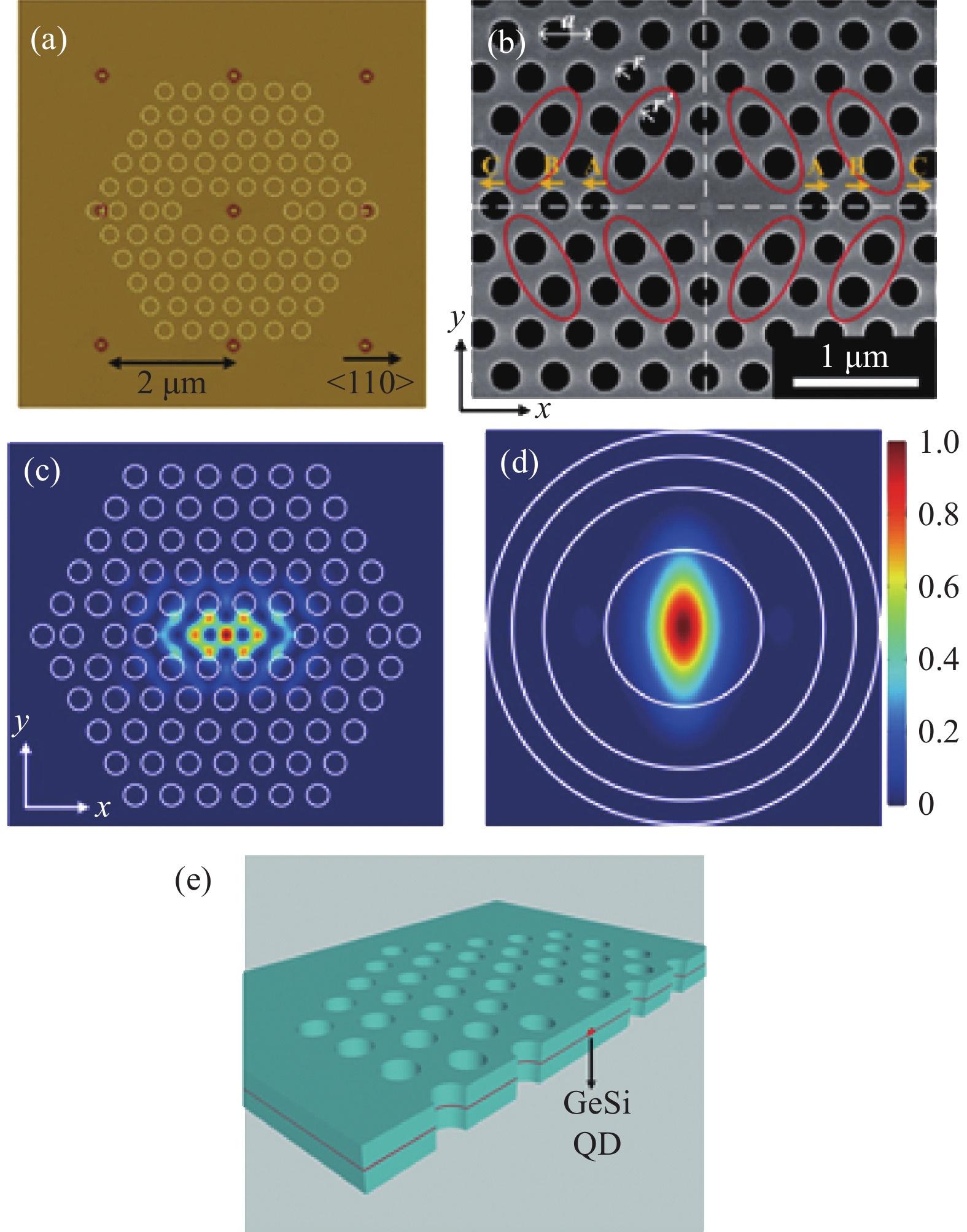
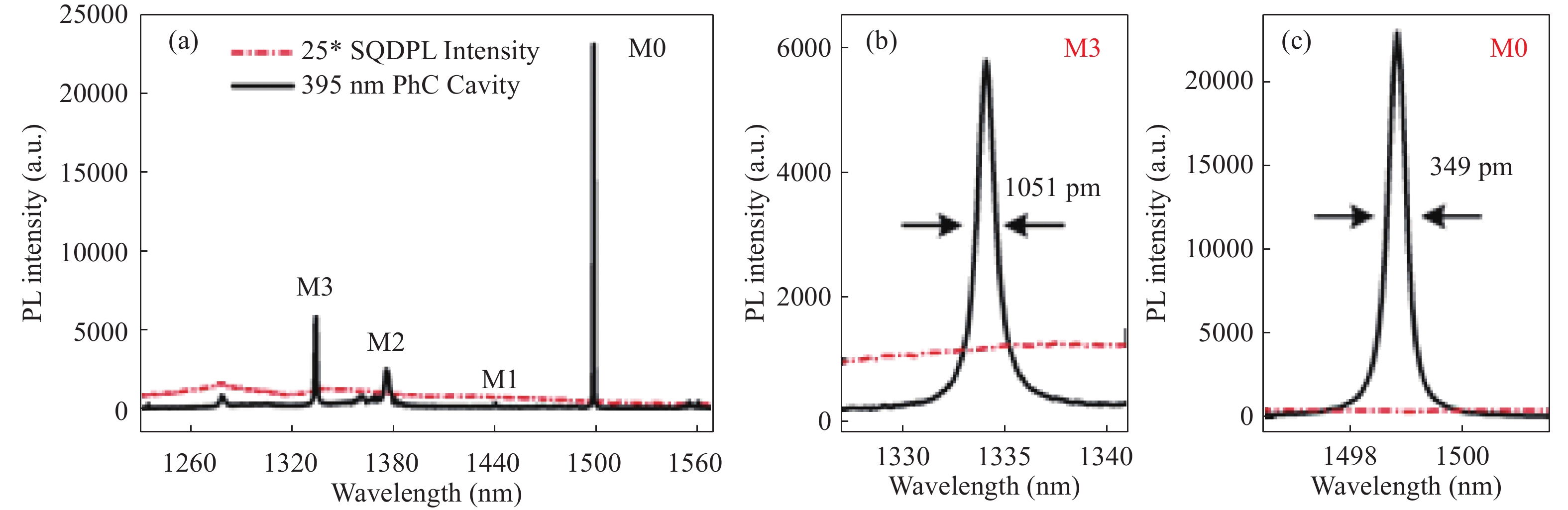
Zeng C, Ma Y J, Zhang Y, et al. Single germanium quantum dot embedded in photonic crystal nanocavity for light emitter on silicon chip. Opt Express, 2015, 23(17): 22250 doi: 10.1364/OE.23.022250 |
| [98] |
Brehm M, Grydlik M. Site-controlled and advanced epitaxial Ge/Si quantum dots: fabrication, properties, and applications. Nanotechnology, 2017, 28(39): 392001 doi: 10.1088/1361-6528/aa8143 |
| [99] |
Du L, Chen G, Lu W. Formation of self-connected Si 0.8Ge 0.2 lateral nanowires and pyramids on rib-patterned Si (1110) substrate. Nanoscale Res Lett, 2017, 12: 70 doi: 10.1186/s11671-016-1820-z |
| [100] |
Zhang J J, Brehm M, Grydlik M, et al. Evolution of epitaxial semiconductor nanodots and nanowires from supersaturated wetting layers. Chem Soc Rev, 2015, 44: 26 doi: 10.1039/C4CS00077C |
| [101] |
Sun X X, Liu J F, Kimerling L C, et al. Direct gap photoluminescence of n-type tensile-strained Ge-on-Si. Appl Phys Lett, 2009, 95(1): 011911 doi: 10.1063/1.3170870 |
| [102] |
Ghetmiri S A, Du W, Margetis J, et al. Direct-bandgap GeSn grown on silicon with 2230 nm photoluminescence. Appl Phys Lett, 2014, 105(15): 151109 doi: 10.1063/1.4898597 |
| [103] |
Wirths S, Geiger R, von den Driesch N, et al. Lasing in direct-bandgap GeSn alloy grown on Si. Nat Photonics, 2015, 9(2): 88 doi: 10.1038/nphoton.2014.321 |
| [104] |
Liu J F, Cannon D D, Wada K, et al. Tensile strained Ge p-i-n photodetectors on Si platform for C and L band telecommunications. Appl Phys Lett, 2005, 87(1): 011110 doi: 10.1063/1.1993749 |


 DownLoad: