


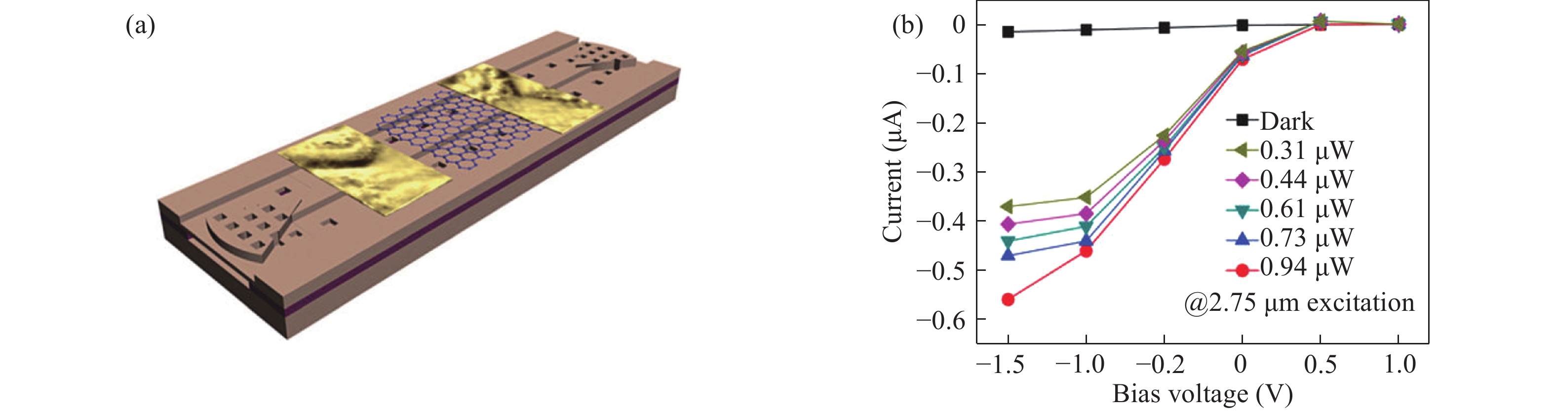
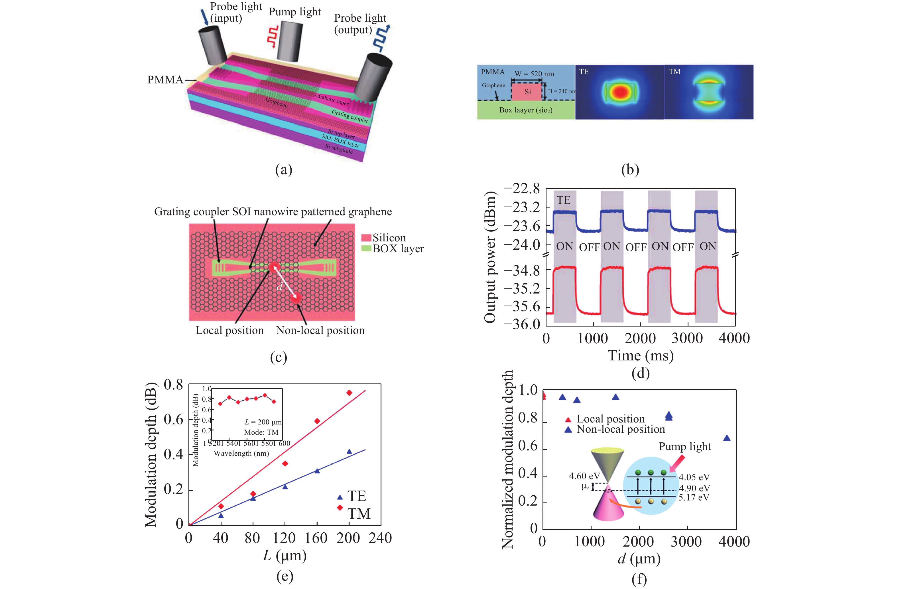
Fig. 1.
(Color online) (a) Schematic of the silicon-graphene waveguide-type photodetector. (b) Measured photocurrent with different input powers (@2.75 μm)[27].
SPECIAL ISSUE ON Si-BASED MATERIALS AND DEVICES
Yanlong Yin1, Jiang Li1, Yang Xu2, Hon Ki Tsang3 and Daoxin Dai1,
Corresponding author: Daoxin Dai, dxdai@zju.edu.cn
Abstract: Silicon photonics has attracted much attention because of the advantages of CMOS (complementary-metal-oxide-semiconductor) compatibility, ultra-high integrated density, etc. Great progress has been achieved in the past decades. However, it is still not easy to realize active silicon photonic devices and circuits by utilizing the material system of pure silicon due to the limitation of the intrinsic properties of silicon. Graphene has been regarded as a promising material for optoelectronics due to its unique properties and thus provides a potential option for realizing active photonic integrated devices on silicon. In this paper, we present a review on recent progress of some silicon-graphene photonic devices for photodetection, all-optical modulation, as well as thermal-tuning.
Key words: silicon, graphene, thermo-optic, all-optic, photodetector
| [1] |
Welch D F, Kish F A, Melle S, et al. Large-scale InP photonic integrated circuits: enabling efficient scaling of optical transport networks. IEEE J Sel Topics Quantum Electron, 2007, 13(1): 22 doi: 10.1109/JSTQE.2006.890068
|
| [2] |
Nicholes S C, Măsanovic M L, Jevremovic B, et al. An 8 × 8 InP monolithic tunable optical router (motor) packet forwarding chip. IEEE J Lightwave Technol, 2010, 28(4): 641 doi: 10.1109/JLT.2009.2030145
|
| [3] |
Shi Y C, Dai D X. Design of a compact multimode interference coupler based on deeply-etched SiO2 ridge waveguides. Optics Commun, 2007, 271(2): 404 doi: 10.1016/j.optcom.2006.10.084
|
| [4] |
Yang L, Yang B, Sheng Z, et al. Compact 2 × 2 tapered multimode interference couplers based on SU-8 polymer rectangular waveguides. Appl Phys Lett, 2008, 93(20): 418
|
| [5] |
Dai D X, He S L. Ultrasmall integrated devices based on silicon nanowires for optical communications. J Nanophotonics, 2008, 2(1): 021780 doi: 10.1117/1.2832772
|
| [6] |
Sheng Z, Dai D X, He S L. Comparative study of losses in ultrasharp silicon-on-insulator nanowire bends. IEEE J Sel Top Quantum Electron, 2009, 15(5): 1406 doi: 10.1109/JSTQE.2009.2013360
|
| [7] |
Wang S P, Feng X L, Gao S M, et al. On-chip reconfigurable optical add-drop multiplexer for hybrid wavelength/ mode-division-multiplexing systems. Opt Lett, 2017, 42(14): 2802 doi: 10.1364/OL.42.002802
|
| [8] |
Chen S T, Wu H, Dai D X. High extinction-ratio compact polarization beam splitter on silicon. Electron Lett, 2016, 52(12): 1043 doi: 10.1049/el.2016.0683
|
| [9] |
Yin Y L, Li Z Y, Dai D X. Ultra-broadband polarization splitter-rotator based on the mode evolution in a dual-core adiabatic taper. IEEE J Lightwave Technol, 2017, 35(11): 2227 doi: 10.1109/JLT.2017.2662200
|
| [10] |
Fu X, Dai D X. Ultra-small Si-nanowire-based 400 GHz-spacing 15 × 15 arrayed-waveguide grating router with microbends. Electron Lett, 2011, 47(4): 266 doi: 10.1049/el.2010.3068
|
| [11] |
Chen P X, Chen S T, Guan X W, et al. High-order microring resonators with bent couplers for a box-like filter response. Opt Lett, 2014, 39(21): 6304 doi: 10.1364/OL.39.006304
|
| [12] |
Wang X K, Guan X W, Huang Q S, et al. Suspended submicron-disk resonator on silicon for optical sensing. Opt Lett, 2013, 38(24): 5405 doi: 10.1364/OL.38.005405
|
| [13] |
Cheng Z Z, Tsang H K. Experimental demonstration of polarization-insensitive air-cladding grating couplers for silicon-on-insulator waveguides. Opt Lett, 2014, 39(7): 2206 doi: 10.1364/OL.39.002206
|
| [14] |
Dai D X, Mao M. Mode converter based on an inverse taper for multimode silicon nanophotonic integrated circuits. Opt Express, 2015, 23(22): 28376 doi: 10.1364/OE.23.028376
|
| [15] |
Fama S, Colace L, Masini G, et al. High performance germanium-on-silicon detectors for optical communications. Appl Phys Lett, 2002, 81(4): 586 doi: 10.1063/1.1496492
|
| [16] |
Kang Y M, Liu H D, Morse M, et al. Monolithic germanium/silicon avalanche photodiodes with 340 GHz gain–bandwidth product. Nat Photon, 2009, 3(1): 59 doi: 10.1038/nphoton.2008.247
|
| [17] |
Fu X, Cheng J X, Huan Q S, et al. 5 × 20 Gb/s heterogeneously integrated III–V on silicon electro-absorption modulator array with arrayed waveguide grating multiplexer. Opt Express, 2015, 23(14): 18686 doi: 10.1364/OE.23.018686
|
| [18] |
Chen S T, Shi Y C, He S L, et al. Low-loss and broadband 2 × 2 silicon thermo-optic Mach–Zehnder switch with bent directional couplers. Opt Lett, 2016, 41(4): 836 doi: 10.1364/OL.41.000836
|
| [19] |
Oulton R F, Sorger V J, Genov D A, et al. A hybrid plasmonic waveguide for subwavelength confinement and long-range propagation. Nat Photonics, 2008, 2(8): 496 doi: 10.1038/nphoton.2008.131
|
| [20] |
Bolotin K, Sikes K, Jiang Z, et al. Ultrahigh electron mobility in suspended graphene. Solid State Commun, 2008, 146(9/10): 351
|
| [21] |
Wan X, Xu Y, Guo H W, et al. A self-powered high-performance graphene/silicon ultraviolet photodetector with ultra-shallow junction: breaking the limit of silicon. NPJ 2D Mater Appl, 2017, 1: 4 doi: 10.1038/s41699-017-0008-4
|
| [22] |
Liu F Z, Kar S. Quantum carrier reinvestment-induced ultrahigh and broadband photocurrent responses in graphene–silicon junctions. ACS Nano, 2014, 8(10): 10270 doi: 10.1021/nn503484s
|
| [23] |
Chen Z F, Cheng Z Z, Wang J Q, et al. High responsivity, broadband, and fast graphene/silicon photodetector in photoconductor mode. Adv Opt Mater, 2015, 3(9): 1207 doi: 10.1002/adom.v3.9
|
| [24] |
Liu J J, Yin Y L, Yu L H, et al. Silicon-graphene conductive photodetector with ultra-high responsivity. Sci Rep, 2017, 7: 40904 doi: 10.1038/srep40904
|
| [25] |
Pospischil A, Humer M, Furchi M M, et al. CMOS-compatible graphene photodetector covering all optical communication bands. Nat Photonics, 2013, 7(11): 892 doi: 10.1038/nphoton.2013.240
|
| [26] |
Gan X T, Shiue R J, Gao Y D, et al. Chip-integrated ultrafast graphene photodetector with high responsivity. Nat Photonics, 2013, 7(11): 883 doi: 10.1038/nphoton.2013.253
|
| [27] |
Wang X M, Cheng Z Z, Xu K, et al. High-responsivity graphene/silicon-heterostructure waveguide photodetectors. Nat Photonics, 2013, 7(11): 888 doi: 10.1038/nphoton.2013.241
|
| [28] |
Yu L H, Zheng J J, Xu Y, et al. Local and nonlocal optically induced transparency effects in graphene–silicon hybrid nanophotonic integrated circuits. ACS Nano, 2014, 8(11): 11386 doi: 10.1021/nn504377m
|
| [29] |
Hendry E, Hale P, Moger J, et al. Coherent nonlinear optical response of graphene. Phys Rev Lett, 2010, 105(9): 097401 doi: 10.1103/PhysRevLett.105.097401
|
| [30] |
Yu L H, He S L, Zheng J J, et al. Graphene-based transparent nano-heater for thermally-tuning silicon nanophotonic integrated devices. Piers Proceedings, 2014
|
| [31] |
Gan S, Cheng C T, Zhan Y H, et al. A highly efficient thermo-optic microring modulator assisted by graphene. Nanoscale, 2015, 7(47): 20249 doi: 10.1039/C5NR05084G
|
| [32] |
Yu L H, Yin Y L, Shi Y C, et al. Thermally tuning silicon photonic micro-disk resonator with graphene transparent nano-heaters. Optica, 2016, 3(2): 159 doi: 10.1364/OPTICA.3.000159
|
| [33] |
Yan Siqi, Zhu Xiaolong, Frandsen L H, et al. Slow-light-enhanced energy efficiency for graphene microheaters on silicon photonic crystal Waveguides. Nat Commun, 2016, 8: 14411 doi: 10.1038/ncomms14411
|
| [34] |
Yu L H L, Dai D X, He S L. Graphene-based transparent flexible heat conductor for thermally tuning nanophotonic integrated devices. Appl Phys Lett, 2014, 105(25): 251104 doi: 10.1063/1.4905002
|
| [35] |
Du X, Skachko I, Barker A, et al. Approaching ballistic transport in suspended graphene. Nat Nanotechnol, 2008, 3(8): 491 doi: 10.1038/nnano.2008.199
|
| [36] |
Bao Q L, Kian P L. Graphene photonics, plasmonics, and broadband optoelectronic devices. ACS Nano, 2012, 6(5): 3677 doi: 10.1021/nn300989g
|
| [37] |
Bonaccorso F, Sun Z, Hasan T, et al. Graphene photonics and optoelectronics. Nat Photonics, 2010, 4(9): 611 doi: 10.1038/nphoton.2010.186
|
| [38] |
Lei S, Nihtianov S. Comparative study of silicon-based ultraviolet photodetectors. IEEE Sens J, 2012, 12(7): 2453 doi: 10.1109/JSEN.2012.2192103
|
| [39] |
Yu T, Wang F, Xu Y, et al. Graphene coupled with silicon quantum dots for high-performance bulk-silicon-based Schottky-junction photodetectors. Adv Mater, 2016, 28(24): 4912 doi: 10.1002/adma.v28.24
|
| [40] |
Xu Y, Ali A, Shehzad K, et al. Solvent-based soft-patterning of graphene lateral heterostructures for broadband high-speed metal–semiconductor–metal photodetectors. Adv Mater Technol, 2017, 2(2): 1600241 doi: 10.1002/admt.201600241
|
| [41] |
Chen Z F, Li X M, Wang J Q, et al. Synergistic effects of plasmonics and electron trapping in graphene short-wave infrared photodetectors with ultrahigh responsivity. ACS Nano, 2017, 11(1): 430 doi: 10.1021/acsnano.6b06172
|
| [42] |
George P, Strait J, Dawlaty J, et al. Ultrafast optical-pump terahertz-probe spectroscopy of the carrier relaxation and recombination dynamics in epitaxial graphene. Nano Lett, 2008, 8(12): 4248 doi: 10.1021/nl8019399
|
| [43] |
Bao Q L, Zhang H, Wang Y, et al. Atomic-layer graphene as a saturable absorber for ultrafast pulsed lasers. Adv Funct Mater, 2009, 19(19): 3077 doi: 10.1002/adfm.v19:19
|
| [44] |
Set S, Yaguchi H, Tanaka Y, et al. Ultrafast fiber pulsed lasers incorporating carbon nanotubes. IEEE J Sel Topics Quantum Electron, 2004, 10(1): 137 doi: 10.1109/JSTQE.2003.822912
|
| [45] |
Scardaci V, Sun Zhipei, Wang F, et al. Carbon nanotube polycarbonate composites for ultrafast lasers. Adv Mater, 2008, 20(21): 4040 doi: 10.1002/adma.v20:21
|
| [46] |
Wang F, Rozhin A G, Scardaci V, et al. Wideband-tuneable, nanotube mode-locked, fibre laser. Nat Nanotechnol, 2008, 3(12): 738 doi: 10.1038/nnano.2008.312
|
| [47] |
Keller U, Weingarten K J, Kartner F X, et al. Semiconductor saturable absorber mirrors (SESAM's) for femtosecond to nanosecond pulse generation in solid-state lasers. IEEE J Sel Top Quantum Electron, 1996, 2(3): 435 doi: 10.1109/2944.571743
|
| [48] |
Huang Q J, Jiang S Z, Chang J, et al. A high-quality, monolayer graphene absorber for a 1.06 μm Q-switched mode-locking Nd: YVO4 laser. Laser Phys, 2013, 23(4): 045807 doi: 10.1088/1054-660X/23/4/045807
|
| [49] |
Lagatsky A, Sun Z, Kulmala T, et al. 2 μm solid-state laser mode-locked by single-layer graphene. Appl Phys Lett, 2013, 102(1): 013113 doi: 10.1063/1.4773990
|
| [50] |
Cafiso S, Ugolotti E, Schmidt A, et al. Sub-100-fs Cr:YAG laser mode-locked by monolayer graphene saturable absorber. Opt Lett, 2013, 38(10): 1745 doi: 10.1364/OL.38.001745
|
| [51] |
Wong C Y, Cheng Z Z, Shi Z R, et al. Mode-locked fiber laser using graphene on silicon waveguide. IEEE International Conference on Group IV Photonics, 2013: 35
|
| [52] |
Zhou L J, Lu L J, Li Z X, et al. Silicon large-scale optical switches using MZIs and dual-ring assisted MZIs. SPIE OPTO, 2016: 97520K
|
| [53] |
Song J F, Fang Q, Tao S H, et al. Fast and low power Michelson interferometer thermo-optical switch on SOI. Opt Express, 2008, 16(20): 15304 doi: 10.1364/OE.16.015304
|
| [54] |
Sohma S, Mino S, Watanabe T, et al. Solid-state optical switches using planar lightwave circuit and IC-on-PLC technologies. Asia-Pacific Opt Commun, 2004: 767
|
| [55] |
Espinola R L, Tsai M C, Yardley J T, et al. Fast and low-power thermooptic switch on thin silicon-on-insulator. IEEE Photonics Technol Lett, 2003, 15(10): 1366 doi: 10.1109/LPT.2003.818246
|
| [56] |
Chu T, Yamada H, Ishida S, et al. Compact 1 × N thermo-optic switches based on silicon photonic wire waveguides. Opt Express, 2005, 13(25): 10109 doi: 10.1364/OPEX.13.010109
|
| [57] |
Van Campenhout J, Green W M J, Vlasov Y A. Design of a digital, ultra-broadband electro-optic switch for reconfigurable optical networks-on-chip. Opt Express, 2009, 17(26): 23793 doi: 10.1364/OE.17.023793
|
| [58] |
Shoji Y, Kintaka K, Suda S, et al. Low-crosstalk 2 × 2 thermo-optic switch with silicon wire waveguides. Opt Express, 2010, 18(9): 9071 doi: 10.1364/OE.18.009071
|
| [59] |
Fang Q, Song J F, Liow T, et al. Ultralow power silicon photonics thermo-optic switch with suspended phase arms. IEEE Photonics Technol Lett, 2011, 23(8): 525 doi: 10.1109/LPT.2011.2114336
|
| [60] |
Suzuki K, Cong G, Tanizawa K, et al. Ultra-high extinction-ratio 2 × 2 silicon optical switch with variable splitter. Opt Express, 2015, 23(7): 9086 doi: 10.1364/OE.23.009086
|
| [61] |
Balandin A A, Ghosh S, Bao W Z, et al. Superior thermal conductivity of single-layer graphene. Nano Lett, 2008, 8(3): 902 doi: 10.1021/nl0731872
|
| [62] |
Dai D X. A novel optical modulators based on multimode optical waveguides. China Patent, 2017201856672
|


Article views: 7873 Times PDF downloads: 356 Times Cited by: 0 Times
Received: 29 September 2017 Revised: 10 December 2017 Online: Accepted Manuscript: 30 January 2018Published: 01 June 2018
| Citation: |
Yanlong Yin, Jiang Li, Yang Xu, Hon Ki Tsang, Daoxin Dai. Silicon-graphene photonic devices[J]. Journal of Semiconductors, 2018, 39(6): 061009. doi: 10.1088/1674-4926/39/6/061009
****
Y L Yin, J Li, Y Xu, H K Tsang, D X Dai. Silicon-graphene photonic devices[J]. J. Semicond., 2018, 39(6): 061009. doi: 10.1088/1674-4926/39/6/061009.

|
| [1] |
Welch D F, Kish F A, Melle S, et al. Large-scale InP photonic integrated circuits: enabling efficient scaling of optical transport networks. IEEE J Sel Topics Quantum Electron, 2007, 13(1): 22 doi: 10.1109/JSTQE.2006.890068
|
| [2] |
Nicholes S C, Măsanovic M L, Jevremovic B, et al. An 8 × 8 InP monolithic tunable optical router (motor) packet forwarding chip. IEEE J Lightwave Technol, 2010, 28(4): 641 doi: 10.1109/JLT.2009.2030145
|
| [3] |
Shi Y C, Dai D X. Design of a compact multimode interference coupler based on deeply-etched SiO2 ridge waveguides. Optics Commun, 2007, 271(2): 404 doi: 10.1016/j.optcom.2006.10.084
|
| [4] |
Yang L, Yang B, Sheng Z, et al. Compact 2 × 2 tapered multimode interference couplers based on SU-8 polymer rectangular waveguides. Appl Phys Lett, 2008, 93(20): 418
|
| [5] |
Dai D X, He S L. Ultrasmall integrated devices based on silicon nanowires for optical communications. J Nanophotonics, 2008, 2(1): 021780 doi: 10.1117/1.2832772
|
| [6] |
Sheng Z, Dai D X, He S L. Comparative study of losses in ultrasharp silicon-on-insulator nanowire bends. IEEE J Sel Top Quantum Electron, 2009, 15(5): 1406 doi: 10.1109/JSTQE.2009.2013360
|
| [7] |
Wang S P, Feng X L, Gao S M, et al. On-chip reconfigurable optical add-drop multiplexer for hybrid wavelength/ mode-division-multiplexing systems. Opt Lett, 2017, 42(14): 2802 doi: 10.1364/OL.42.002802
|
| [8] |
Chen S T, Wu H, Dai D X. High extinction-ratio compact polarization beam splitter on silicon. Electron Lett, 2016, 52(12): 1043 doi: 10.1049/el.2016.0683
|
| [9] |
Yin Y L, Li Z Y, Dai D X. Ultra-broadband polarization splitter-rotator based on the mode evolution in a dual-core adiabatic taper. IEEE J Lightwave Technol, 2017, 35(11): 2227 doi: 10.1109/JLT.2017.2662200
|
| [10] |
Fu X, Dai D X. Ultra-small Si-nanowire-based 400 GHz-spacing 15 × 15 arrayed-waveguide grating router with microbends. Electron Lett, 2011, 47(4): 266 doi: 10.1049/el.2010.3068
|
| [11] |
Chen P X, Chen S T, Guan X W, et al. High-order microring resonators with bent couplers for a box-like filter response. Opt Lett, 2014, 39(21): 6304 doi: 10.1364/OL.39.006304
|
| [12] |
Wang X K, Guan X W, Huang Q S, et al. Suspended submicron-disk resonator on silicon for optical sensing. Opt Lett, 2013, 38(24): 5405 doi: 10.1364/OL.38.005405
|
| [13] |
Cheng Z Z, Tsang H K. Experimental demonstration of polarization-insensitive air-cladding grating couplers for silicon-on-insulator waveguides. Opt Lett, 2014, 39(7): 2206 doi: 10.1364/OL.39.002206
|
| [14] |
Dai D X, Mao M. Mode converter based on an inverse taper for multimode silicon nanophotonic integrated circuits. Opt Express, 2015, 23(22): 28376 doi: 10.1364/OE.23.028376
|
| [15] |
Fama S, Colace L, Masini G, et al. High performance germanium-on-silicon detectors for optical communications. Appl Phys Lett, 2002, 81(4): 586 doi: 10.1063/1.1496492
|
| [16] |
Kang Y M, Liu H D, Morse M, et al. Monolithic germanium/silicon avalanche photodiodes with 340 GHz gain–bandwidth product. Nat Photon, 2009, 3(1): 59 doi: 10.1038/nphoton.2008.247
|
| [17] |
Fu X, Cheng J X, Huan Q S, et al. 5 × 20 Gb/s heterogeneously integrated III–V on silicon electro-absorption modulator array with arrayed waveguide grating multiplexer. Opt Express, 2015, 23(14): 18686 doi: 10.1364/OE.23.018686
|
| [18] |
Chen S T, Shi Y C, He S L, et al. Low-loss and broadband 2 × 2 silicon thermo-optic Mach–Zehnder switch with bent directional couplers. Opt Lett, 2016, 41(4): 836 doi: 10.1364/OL.41.000836
|
| [19] |
Oulton R F, Sorger V J, Genov D A, et al. A hybrid plasmonic waveguide for subwavelength confinement and long-range propagation. Nat Photonics, 2008, 2(8): 496 doi: 10.1038/nphoton.2008.131
|
| [20] |
Bolotin K, Sikes K, Jiang Z, et al. Ultrahigh electron mobility in suspended graphene. Solid State Commun, 2008, 146(9/10): 351
|
| [21] |
Wan X, Xu Y, Guo H W, et al. A self-powered high-performance graphene/silicon ultraviolet photodetector with ultra-shallow junction: breaking the limit of silicon. NPJ 2D Mater Appl, 2017, 1: 4 doi: 10.1038/s41699-017-0008-4
|
| [22] |
Liu F Z, Kar S. Quantum carrier reinvestment-induced ultrahigh and broadband photocurrent responses in graphene–silicon junctions. ACS Nano, 2014, 8(10): 10270 doi: 10.1021/nn503484s
|
| [23] |
Chen Z F, Cheng Z Z, Wang J Q, et al. High responsivity, broadband, and fast graphene/silicon photodetector in photoconductor mode. Adv Opt Mater, 2015, 3(9): 1207 doi: 10.1002/adom.v3.9
|
| [24] |
Liu J J, Yin Y L, Yu L H, et al. Silicon-graphene conductive photodetector with ultra-high responsivity. Sci Rep, 2017, 7: 40904 doi: 10.1038/srep40904
|
| [25] |
Pospischil A, Humer M, Furchi M M, et al. CMOS-compatible graphene photodetector covering all optical communication bands. Nat Photonics, 2013, 7(11): 892 doi: 10.1038/nphoton.2013.240
|
| [26] |
Gan X T, Shiue R J, Gao Y D, et al. Chip-integrated ultrafast graphene photodetector with high responsivity. Nat Photonics, 2013, 7(11): 883 doi: 10.1038/nphoton.2013.253
|
| [27] |
Wang X M, Cheng Z Z, Xu K, et al. High-responsivity graphene/silicon-heterostructure waveguide photodetectors. Nat Photonics, 2013, 7(11): 888 doi: 10.1038/nphoton.2013.241
|
| [28] |
Yu L H, Zheng J J, Xu Y, et al. Local and nonlocal optically induced transparency effects in graphene–silicon hybrid nanophotonic integrated circuits. ACS Nano, 2014, 8(11): 11386 doi: 10.1021/nn504377m
|
| [29] |
Hendry E, Hale P, Moger J, et al. Coherent nonlinear optical response of graphene. Phys Rev Lett, 2010, 105(9): 097401 doi: 10.1103/PhysRevLett.105.097401
|
| [30] |
Yu L H, He S L, Zheng J J, et al. Graphene-based transparent nano-heater for thermally-tuning silicon nanophotonic integrated devices. Piers Proceedings, 2014
|
| [31] |
Gan S, Cheng C T, Zhan Y H, et al. A highly efficient thermo-optic microring modulator assisted by graphene. Nanoscale, 2015, 7(47): 20249 doi: 10.1039/C5NR05084G
|
| [32] |
Yu L H, Yin Y L, Shi Y C, et al. Thermally tuning silicon photonic micro-disk resonator with graphene transparent nano-heaters. Optica, 2016, 3(2): 159 doi: 10.1364/OPTICA.3.000159
|
| [33] |
Yan Siqi, Zhu Xiaolong, Frandsen L H, et al. Slow-light-enhanced energy efficiency for graphene microheaters on silicon photonic crystal Waveguides. Nat Commun, 2016, 8: 14411 doi: 10.1038/ncomms14411
|
| [34] |
Yu L H L, Dai D X, He S L. Graphene-based transparent flexible heat conductor for thermally tuning nanophotonic integrated devices. Appl Phys Lett, 2014, 105(25): 251104 doi: 10.1063/1.4905002
|
| [35] |
Du X, Skachko I, Barker A, et al. Approaching ballistic transport in suspended graphene. Nat Nanotechnol, 2008, 3(8): 491 doi: 10.1038/nnano.2008.199
|
| [36] |
Bao Q L, Kian P L. Graphene photonics, plasmonics, and broadband optoelectronic devices. ACS Nano, 2012, 6(5): 3677 doi: 10.1021/nn300989g
|
| [37] |
Bonaccorso F, Sun Z, Hasan T, et al. Graphene photonics and optoelectronics. Nat Photonics, 2010, 4(9): 611 doi: 10.1038/nphoton.2010.186
|
| [38] |
Lei S, Nihtianov S. Comparative study of silicon-based ultraviolet photodetectors. IEEE Sens J, 2012, 12(7): 2453 doi: 10.1109/JSEN.2012.2192103
|
| [39] |
Yu T, Wang F, Xu Y, et al. Graphene coupled with silicon quantum dots for high-performance bulk-silicon-based Schottky-junction photodetectors. Adv Mater, 2016, 28(24): 4912 doi: 10.1002/adma.v28.24
|
| [40] |
Xu Y, Ali A, Shehzad K, et al. Solvent-based soft-patterning of graphene lateral heterostructures for broadband high-speed metal–semiconductor–metal photodetectors. Adv Mater Technol, 2017, 2(2): 1600241 doi: 10.1002/admt.201600241
|
| [41] |
Chen Z F, Li X M, Wang J Q, et al. Synergistic effects of plasmonics and electron trapping in graphene short-wave infrared photodetectors with ultrahigh responsivity. ACS Nano, 2017, 11(1): 430 doi: 10.1021/acsnano.6b06172
|
| [42] |
George P, Strait J, Dawlaty J, et al. Ultrafast optical-pump terahertz-probe spectroscopy of the carrier relaxation and recombination dynamics in epitaxial graphene. Nano Lett, 2008, 8(12): 4248 doi: 10.1021/nl8019399
|
| [43] |
Bao Q L, Zhang H, Wang Y, et al. Atomic-layer graphene as a saturable absorber for ultrafast pulsed lasers. Adv Funct Mater, 2009, 19(19): 3077 doi: 10.1002/adfm.v19:19
|
| [44] |
Set S, Yaguchi H, Tanaka Y, et al. Ultrafast fiber pulsed lasers incorporating carbon nanotubes. IEEE J Sel Topics Quantum Electron, 2004, 10(1): 137 doi: 10.1109/JSTQE.2003.822912
|
| [45] |
Scardaci V, Sun Zhipei, Wang F, et al. Carbon nanotube polycarbonate composites for ultrafast lasers. Adv Mater, 2008, 20(21): 4040 doi: 10.1002/adma.v20:21
|
| [46] |
Wang F, Rozhin A G, Scardaci V, et al. Wideband-tuneable, nanotube mode-locked, fibre laser. Nat Nanotechnol, 2008, 3(12): 738 doi: 10.1038/nnano.2008.312
|
| [47] |
Keller U, Weingarten K J, Kartner F X, et al. Semiconductor saturable absorber mirrors (SESAM's) for femtosecond to nanosecond pulse generation in solid-state lasers. IEEE J Sel Top Quantum Electron, 1996, 2(3): 435 doi: 10.1109/2944.571743
|
| [48] |
Huang Q J, Jiang S Z, Chang J, et al. A high-quality, monolayer graphene absorber for a 1.06 μm Q-switched mode-locking Nd: YVO4 laser. Laser Phys, 2013, 23(4): 045807 doi: 10.1088/1054-660X/23/4/045807
|
| [49] |
Lagatsky A, Sun Z, Kulmala T, et al. 2 μm solid-state laser mode-locked by single-layer graphene. Appl Phys Lett, 2013, 102(1): 013113 doi: 10.1063/1.4773990
|
| [50] |
Cafiso S, Ugolotti E, Schmidt A, et al. Sub-100-fs Cr:YAG laser mode-locked by monolayer graphene saturable absorber. Opt Lett, 2013, 38(10): 1745 doi: 10.1364/OL.38.001745
|
| [51] |
Wong C Y, Cheng Z Z, Shi Z R, et al. Mode-locked fiber laser using graphene on silicon waveguide. IEEE International Conference on Group IV Photonics, 2013: 35
|
| [52] |
Zhou L J, Lu L J, Li Z X, et al. Silicon large-scale optical switches using MZIs and dual-ring assisted MZIs. SPIE OPTO, 2016: 97520K
|
| [53] |
Song J F, Fang Q, Tao S H, et al. Fast and low power Michelson interferometer thermo-optical switch on SOI. Opt Express, 2008, 16(20): 15304 doi: 10.1364/OE.16.015304
|
| [54] |
Sohma S, Mino S, Watanabe T, et al. Solid-state optical switches using planar lightwave circuit and IC-on-PLC technologies. Asia-Pacific Opt Commun, 2004: 767
|
| [55] |
Espinola R L, Tsai M C, Yardley J T, et al. Fast and low-power thermooptic switch on thin silicon-on-insulator. IEEE Photonics Technol Lett, 2003, 15(10): 1366 doi: 10.1109/LPT.2003.818246
|
| [56] |
Chu T, Yamada H, Ishida S, et al. Compact 1 × N thermo-optic switches based on silicon photonic wire waveguides. Opt Express, 2005, 13(25): 10109 doi: 10.1364/OPEX.13.010109
|
| [57] |
Van Campenhout J, Green W M J, Vlasov Y A. Design of a digital, ultra-broadband electro-optic switch for reconfigurable optical networks-on-chip. Opt Express, 2009, 17(26): 23793 doi: 10.1364/OE.17.023793
|
| [58] |
Shoji Y, Kintaka K, Suda S, et al. Low-crosstalk 2 × 2 thermo-optic switch with silicon wire waveguides. Opt Express, 2010, 18(9): 9071 doi: 10.1364/OE.18.009071
|
| [59] |
Fang Q, Song J F, Liow T, et al. Ultralow power silicon photonics thermo-optic switch with suspended phase arms. IEEE Photonics Technol Lett, 2011, 23(8): 525 doi: 10.1109/LPT.2011.2114336
|
| [60] |
Suzuki K, Cong G, Tanizawa K, et al. Ultra-high extinction-ratio 2 × 2 silicon optical switch with variable splitter. Opt Express, 2015, 23(7): 9086 doi: 10.1364/OE.23.009086
|
| [61] |
Balandin A A, Ghosh S, Bao W Z, et al. Superior thermal conductivity of single-layer graphene. Nano Lett, 2008, 8(3): 902 doi: 10.1021/nl0731872
|
| [62] |
Dai D X. A novel optical modulators based on multimode optical waveguides. China Patent, 2017201856672
|

 WeChat ID
Journal of Semiconductors © 2017 All Rights Reserved 京ICP备05085259号-2

 DownLoad:

