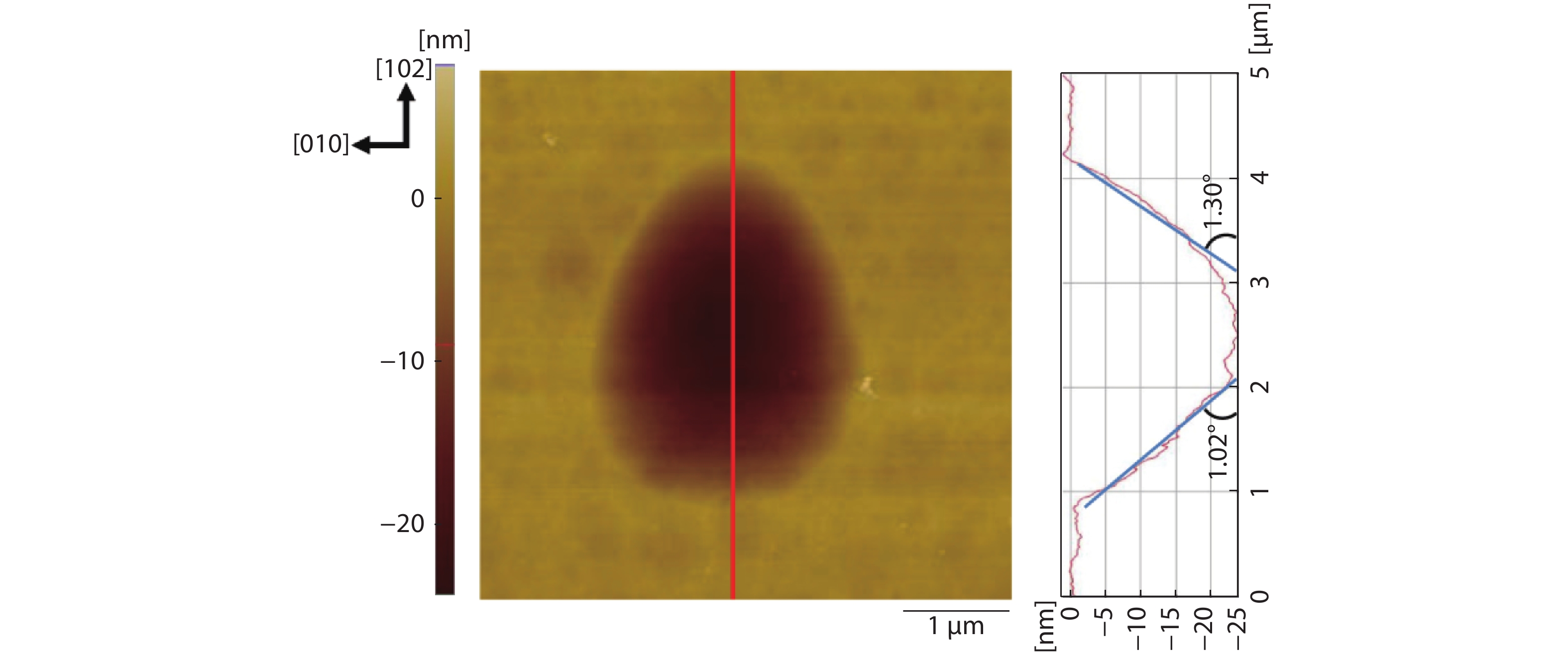
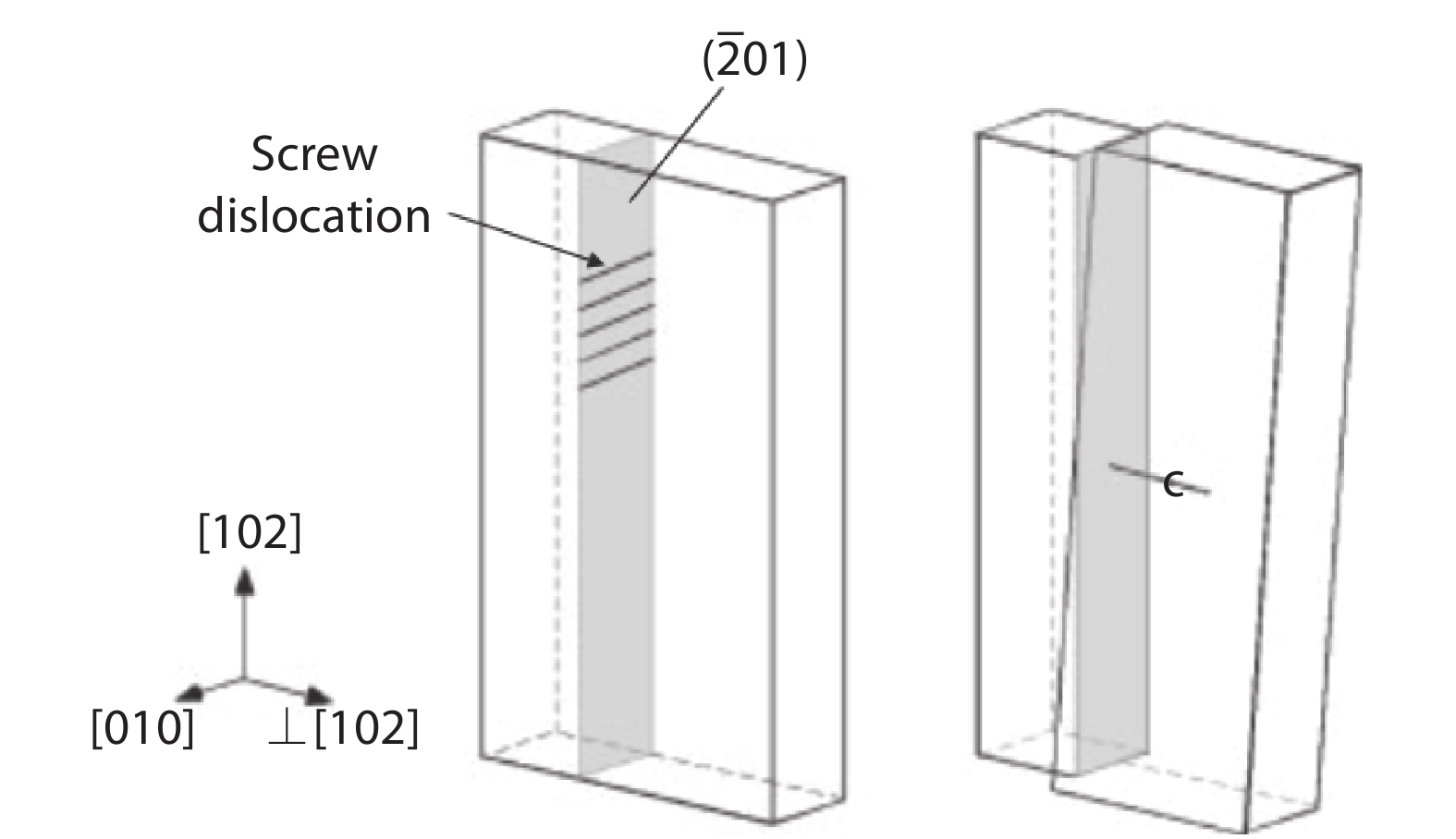
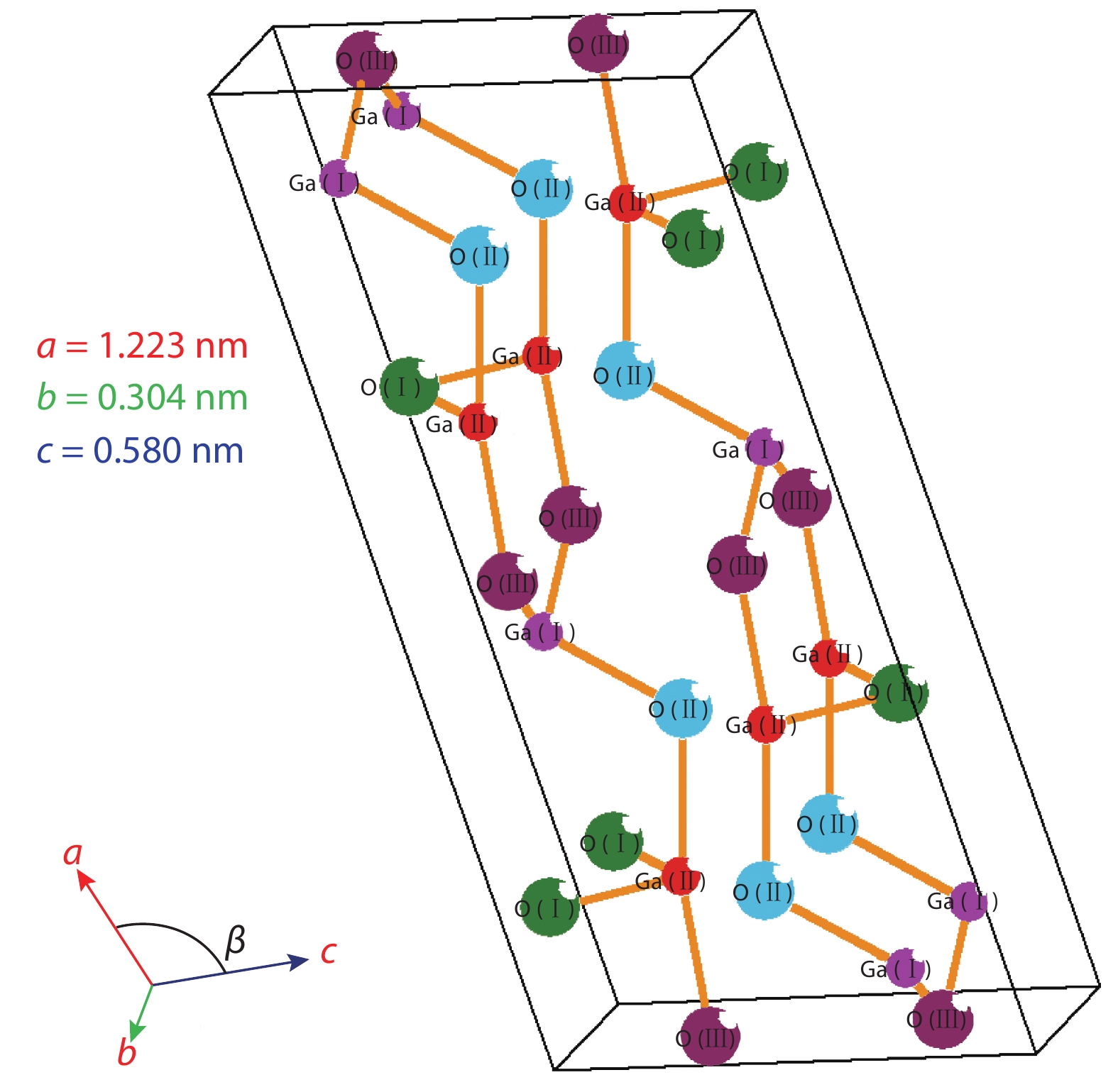
Loading [MathJax]/jax/output/HTML-CSS/jax.js
J. Semicond. > 2019, Volume 40 > Issue 1 > 011804

REVIEWS

A review of β-Ga2O3 single crystal defects, their effects on device performance and their formation mechanism

Bo Fu, Zhitai Jia, Wenxiang Mu, Yanru Yin, Jian Zhang and Xutang Tao

+ Author Affiliations

 Corresponding author: Zhitai Jia, Email: z.jia@sdu.edu.cn; Xutang Tao, txt@sdu.edu.cn

DOI: 10.1088/1674-4926/40/1/011804

PDF

Turn off MathJax

Abstract: As a wide-bandgap semiconductor (WBG), β-Ga2O3 is expected to be applied to power electronics and solar blind UV photodetectors. In this review, defects in β-Ga2O3 single crystals were summarized, including dislocations, voids, twin, and small defects. Their effects on device performance were discussed. Dislocations and their surrounding regions can act as paths for the leakage current of SBD in single crystals. However, not all voids lead to leakage current. There’s no strong evidence yet to show small defects affect the electrical properties. Doping impurity was definitely irrelated to the leakage current. Finally, the formation mechanism of the defects was analyzed. Most small defects were induced by mechanical damages. The screw dislocation originated from a subgrain boundary. The edge dislocation lying on a plane slightly tilted towards the (102) plane, the (101) being the possible slip plane. The voids defects like hollow nanopipes, PNPs, NSGs and line-shaped grooves may be caused by the condensation of excess oxygen vacancies, penetration of tiny bubbles or local meltback. The nucleation of twin lamellae occurred at the initial stage of " shoulder part” during the crystal growth. These results are helpful in controlling the occurrence of crystal defects and improving the device performance.

Key words: β-Ga2O3crystal defectsdevice performanceformation mechanism

Recently, β-Ga2O3 has attracted great attention as an ultra wide band-gap oxide semiconductor for future power and photodetector devices. In order to achieve high-performance and high-reliability of semiconductor devices, it is critical to control crystal defects because those defects could have negative and damaging effects on the device performance. In some cases, those crystal defects can even bring about leakage current and lower breakdown voltage, such as micropipes observed in SiC. Thus, it is essential to characterize defects in the crystal and understand their formation mechanism.

The crystal structure of β-Ga2O3 is shown in Fig. 1. β-Ga2O3 is the most thermodynamically stable one in terms of the six different phases of the α, β, γ, δ, ε, and φ phases[1]. β-Ga2O3 belongs to monoclinic system with lattice constants of a = 1.223 nm, b = 0.304 nm, and c = 0.580 nm, and the angle between the a- and c-axes is β = 103.7°[2]. There exist two inequivalent Ga sites and three inequivalent O sites, denoted by Ga(I), Ga(II), O(I), O(II), and O(III) atoms, respectively. Ga(I) atoms form slightly distorted tetrahedral bonds with 4 O ions, and Ga(II) atoms form a highly distorted cubic close packing arrangement with 6 neighboring O ions. O(I) and O(II) are 3-fold-coordinated, whereas O(III) is 4-fold-coordinated at the corner of three octahedra and one tetrahedron[35].

Figure  1.  (Color online) Monoclinic unit cell of β-Ga2O3 and relative lattice parameters.

The melting point of Ga2O3 is approximately 1800 °C[36]. In order to obtain large size crystal combined with high structural quality, melt growth methods are the most suitable, especially when they are used for industrial production. A few melt growth techniques have been used to grow bulk β-Ga2O3 single crystals successfully, such as Verneuil[68], Optical Floating Zone (OFZ)[911], Vertical Bridgman (VB)/Vertical Gradient Freeze (VGF)[12, 13], Edge-Defined Film-Fed Growth (EFG)[1417] and the Czochralski methods[1823]. The flux[24, 25] and gas phase[26, 27] methods have also been applied to the growth of β-Ga2O3. However, the obtained crystal size is too small for applications, so these methods are not considered here. Similarly, the Verneuil method is also not introduced in this review considering the imperfect β-Ga2O3 crystal quality and inadequate crystal size (only 10 mm in diameter).

Fig. 2 showed the examples of bulk β-Ga2O3 single crystals obtained by melt growth methods: (a) EFG, (b) VB, (c) Czochralski and (d) OFZ. The EFG method employs a die or a shaper that is placed in a metal crucible. The melt is transported from the crucible to a shaped top surface of the die by a narrow slit or channel due to capillary forces. The growth direction is always along the [010] crystallographic direction, which is paralleled to both cleavage planes (100) and (001). Presently, the EFG method is able to fabricate substrate of 2″ (commercialized), 4″ (demonstrated), and possible 6″ (under research & development) as shown in Fig. 2(a). The VB method utilizing a Pt-Rh (70%–30%) alloy crucible to grow β-Ga2O3 single crystal is in development, which is favorable for high oxygen concentration. The crystal of 25 mm in diameter is grown in air without a crystal seed as shown in Fig. 2(b). As for the crystal growth by Czochralski method, crystal spiral growth turns out to be the main challenge. However, the novel approach with a CO2-containing growth atmosphere providing oxygen partial pressures, allows to obtain 2″ in diameter crystals as shown in Fig. 2(c). The OFZ method is a crucible-free technique. The main advantage of this method is the possibility of using highly oxidizing atmosphere to suppress the volatilization of β-Ga2O3. Crystals with 1 in. diameter have been reported as shown in Fig. 2(d).

Figure  2.  (Color online) Bulk β-Ga2O3 crystals obtained by the following melt methods: (a) EFG, (b) VB, (c) Czochralski, and (d) OFZ. Copyright 2017 ECS Journal of Solid State Science and Technology[28]. Copyright 2016 J Cryst Growth[13]. Copyright 2014 J Cryst Growth[47]. Copyright 2004 J Cryst Growth[11].

β-Ga2O3 has attracted much interest as a substrate to grow GaN heteroepitaxy for efficient high-brightness vertically-structured LEDs due to its good conductivity and nice transparency[30, 31]. In addition, its most potential application fields are solar-blind UV photodetectors and high power devices. Because of its ultra wide band gap, 4.9 eV, β-Ga2O3 is highly transparent from the visible to the deep UV region and has an extremely high theoretical breakdown electric field (Ebr) of 8 MV/cm[32]. The potential advantage of β-Ga2O3 is well described by the Baliga's figure of merit (BFOM) which indicates its basic suitability as a semiconductor material for high power applications[2]. β-Ga2O3 has a BFOM about 3000, 10 and 4 times higher than that of Si, SiC and GaN, respectively. This result is graphically depicted in Fig. 3, which showed the theoretical limits of the on-resistance as a function of breakdown voltage for the most studied semiconductors. Due to a much higher BFOM, β-Ga2O3 is predicted to outperform SiC and GaN, meanwhile exceeds the physical limits of Si for power switching applications[33]. Despite of the relatively low electron mobility limited to 200 cm2V−1s−1 by calculation[34], the drastic reduction of the distance between gate and drain will allow the fabrication of high efficient semiconductor switches. Furthermore, compared with SiC and GaN[35], β-Ga2O3 has a relatively low thermal conductivity. Therefore, the development of thermally stable metal contacts and passivation layers would make up for this disadvantage and allow β-Ga2O3-based power electronics to operate under comparatively high temperature.

Figure  3.  (Color online) Theoretical limits of on-resistance versus breakdown voltage in unipolar power devices for β-Ga2O3 and other major semiconductors. Copyright 2014 Physical Status Solidi[29].

In this review, we summarize all kinds of defects observed in β-Ga2O3 single crystal recently. Subsequently, the effects of defects on device performance and their formation mechanism are summarized and analyzed in detail, which will provide a basis reference for device performance improvement in the future.

The dislocations can be divided into two types, screw dislocation and edge dislocation. Nakai et al. found out the screw dislocations on the (010) plane[38], as shown in Fig. 4. The dislocation under etch pit was almost paralleled to [010]. The etch pits of dislocation were approximately 2μm in length and 106–107 cm−2 in density. Most of etch pits align in rows along [100] and [102]. According to the gb invisibility criterion[42], the Burgers vector of dislocations were determined to parallel to [010]. Therefore, the dislocation was defined as screw dislocation because the Burgers vector and dislocation were both paralleled to [010] direction.

Figure  4.  Cross-sectional TEM image of a dislocation viewed from [ ˉ10ˉ2 ]. Copyright 2015 Jpn J Appl Phys[38].

Ueda et al. reported the edge dislocation on the ( ˉ201 ) plane[39], as shown in Fig. 5. The etch pits of edge dislocation mostly lied in a row along the [010] direction as shown in Fig. 5(a). The estimated etch pit density was 104 cm−2. The distance between the etch pits varied in the range 20–100μm. Apart from these pits, isolated etch pits were also observed as shown in Fig. 5(b). The result suggested that the etch pit was four-faceted with a core inside, the surface being rectangular in shape. Its long axis was in the [102] direction. The core of the etch pit was slightly off-centered. According to gb invisibility criterion similar to the determination of screw dislocation, it can be clearly indicated that the defect under the etch pit was an edge dislocation because the Burgers vector was perpendicular to dislocation direction.

Figure  5.  (Color online) (a) Optical micrograph of surface of ( ˉ201 ) plane after etching. (b) Enlarged image of the etch pits. An XTEM sample is indicated by a white line. Copyright 2016 Jpn J Appl Phys[39].

The voids defect has some volume, and thus can be observed on different crystal planes, including hollow nanopipes[38], platelike nanopipes (PNPs)[39], nanometer-sized grooves (NSGs)[40] and line-shaped grooves[44]. Nanopipes were hollow characterized by electron diffraction patterns and EDS. Its size was 0.1 μm in diameter and at least 15 μm in length elongated along [010] because the bottom end of the defect was not located in the TEM sample, as shown in Fig. 6. No strain field was found around them. The etch pits distribution of hollow nanopipes showed no significant orientation, with a density of 102 cm−2.

Figure  6.  Cross-sectional TEM image of a hollow nanopipes defect viewed from [ ˉ10ˉ2 ]. Copyright 2015 Jpn J Appl Phys[38].

A very narrow groove[39] goes deep into the crystal, thus, the defect is called platelike nanopie on the (010) plane as shown in Fig. 7(a) which is different from hollow nanopipe in Fig. 6. The etch pits of PNPs was along the (010) plane and parallelogram-shaped. The PNPs was hollow, too. In addition, Nanometer-sized grooves also were found on the (010) plane[40]. The NSGs length ranged from 50–1200 nm in the [001] direction, and the width of most grooves was approximately 40 nm in the [100] direction as shown inFig. 7(b). The main sidewalls in the grooves were (100) and (001) because they were both thermodynamically stable planes. These NSGs tended to be generated along the [001] direction. All NSGs should terminate within crystal because the grooves disappeared gradually with the etching time. The depth was estimated to be roughly 30 nm. The NSGs were different from micropipes found in SiC crystal[37, 41] that penetrate the whole crystal.

Figure  7.  (a) A cross-sectional FIB-SIM image of an PNPs defects. Copyright 2016 Jpn J Appl Phys[39]. (b) SEM image of three NSGs in an array along the [001] direction. Copyright 2016 Jpn J Appl Phys[40].

Numerous line-shaped grooves[44] extended along the [010] direction and broadened along the [100] direction on the (001) plane as shown inFig. 8. Such line-shaped defects existed not only on the etched surface but also inside the crystal, and can be regarded as voids because these defects had some volume. The etched line-shaped grooves density near the surface was approximately 3 × 102 cm−2. The length of the grooves along [010] varied from 10–400 μm. In addition, a line-shaped etch pattern was also found on the ( ˉ201 ) plane by Kasu et al.[45]. The defect was the same as those observed by Kuramata et al.[46].

Figure  8.  (Color online) DICM images showing line-shaped voids exposed on the surface etching for (a) 5 min and (b) 25 min. (c) Length histogram of the 625 line-shaped voids observed on the 5-min etched surface. Copyright 2017 Jpn J Appl Phys[44].

A large number of defects were reported on (010), (001), and ( ˉ201 ) crystal planes. In contrast, the defects reported on (100) is very rare. Galazka et al. even considered the (100) plane as almost dislocation-free plane because the dislocations were all parallel to the (100) cleavage plane and did not lead to etch pits on (100) surface at all[47]. However, an important defect, twin, was observed on the (100) plane[39]. The shapes of the etch pits corresponding to the defects of PNPs on both sides of the dotted line had mirror symmetry. The plane corresponding to the dotted line was a (100) twin boundary also shown in Fig. 9(a). A schematic diagram of the atomic structure of the twin lamellae is shown in Fig. 9(b).

Figure  9.  (a) An SEM image of etched surface of ( 0ˉ10 ) plane including a twin boundary. (b) The atomic structure of a region including a twin lamellae in β-Ga2O3 crystal viewed from the ( 0ˉ10 ) direction. Copyright 2016 Jpn J Appl Phys[39].

Apart from the mentioned defects above, small defects were also found. However, the small defects exist in the shape of different types of etch pits, including arrow-shaped etch pit[44, 45] and gourd-shaped etch pit[45]. The arrow’s head faced toward the [102] direction. Some of the etch pits tended to form an array toward the [010] direction.Fig. 10 showed an AFM image of the arrow-shaped etch pit. The average density was 7 × 104 cm−2. The depth of the etch pit was approximately 600 nm. The origin of the arrow-shaped etch pit was predicted to be from a dislocation.

Figure  10.  (Color online) AFM images of an arrow-shaped etch pit. Copyright 2017 Jpn J Appl Phys[45].

Fig. 11 showed the AFM image of a gourd-shaped etch pit. The point head faced toward the [102] direction. The average density was 9 × 104 cm−2. The depth of the gourd-shaped etch pit was 25 nm, which was much less than that of the arrow-shaped etch pit (600 nm). Thus, the gourd-shaped etch pit tended to be shallower than the arrow-shaped etch pit. Some gourd-shaped etch pits also tended to form an array along the [010] direction. The origin of the gourd-shaped etch pit should be a dislocation similar to the arrow-shaped etch pit.

Figure  11.  (Color online) AFM image of a gourd-shaped etch pit. Copyright 2017 Jpn J Appl Phys[45].

Furthermore, Hanada et al.[43] pointed out that etch pits of various shapes were observed on (010) plane and divided into types A-G according to the shape of etch pits as shown in Figs. 12 and 13. The type-A etch pit became type-B etch pit after etching for 10 min, and subsequently became the type-C etch pit after further etching for 10 min. Finally, the type-C etch pit changed to type-D after etching for 20 more min. Therefore, it could be concluded that type A, B, C, and D originate from void-type crystal defects. The type-G void defect could become type-A etch pit after etching as shown in Fig. 13. Thus, the void defects must change in shape similar to type-G→A→B→C→D etch pits by etching. In addition, the size of the type-E and type-F etch pit increased after etching, nevertheless, the shape remained unchanged. This suggested that the type-E and type-F etch pit contained a dislocation as its core in the depth direction.

Figure  12.  SEM images of six etch pits of different shapes (Types A, B, C, D, E, and F) according to shapes of the etch pits on β-Ga2O3 (010) single crystal surface. Copyright 2016 Jpn J Appl Phys.[43]
Figure  13.  SEM images of the same pit at the same position on the same β-Ga2O3 (010) single crystal surface etched for the etching times of 0, 2, 4, and 10 min. Copyright 2016 Jpn J Appl Phys[43].

Table 1 covers all types of defects, except small defects [discussed in 3.2], observed on different β-Ga2O3 crystal planes. Actually, in terms of defects features, these defects can be classified into three types: (1) dislocation (edge dislocation and screw dislocation),(2) defects that originated from voids (hollow nanopipes, PNPs, NSGs, line-shaped grooves), (3) twin. The Burgers vector of edge and screw dislocation observed on ( ˉ201 ) and (010) respectively are both paralleled to [010] direction. However, the distribution direction of etch pits and the dislocation extending direction are completely different. In addition, it is found that the extending direction of void defects are all paralleled to the [010] direction. The etch pits distribution of PNPs and NSGs observed on (010) lie in rows along [100] and [001] direction, respectively. Furthermore, the etch pits distribution of hollow nanopipes and line-shaped grooves observed on (010) and ( ˉ201 ), (001) respectively do not show significant direction. The twin crystal found on ( 0ˉ10 ) is the (100) crystal plane.

Table  1.  All kinds of defects observed on different β-Ga2O3 crystal plane.
Parameter Edge dislocation Screw dislocation Twin Hollow nanopipes PNPs NSGs Line-shaped grooves
Crystal plane ( {\bar{2}01} $) (010) ( 0ˉ10) (010) (010) (010) ( ˉ201)(001)
Crystal direction //[010] //[100]//[102] No direction //[100] //[001] No direction
Dislocation direction Not exactly normal to ( ˉ201) but
slightly tilting to [102]
//[010]
Burgers vector //[010] //[010]
Twin plane (100)
Void direction //[010] //[010] //[010] //[010]
DownLoad: CSV  | Show Table

In this section, four types of defects have been found in β-Ga2O3, and their effects on device performance are to be summarized. The effects on device performances caused by dislocation and void have been discussed by Kasu et al.[48] Fig. 14(a) showed the relationship between the number of dislocations and the reverse leakage current (IR) in SBD. In this figure, the reverse leakage current at −15 V was represented by the colors of the circles. The black, yellow, and red circles indicated low, intermediate, and high reverse leakage currents (IR), respectively. They found that in the rich dislocation region at the upper center to the middle right of the sample, the reverse leakage current (IR) was high, which suggested that there was a strong relationship between the number of dislocations and the reverse leakage current. Dislocations were considered to run mainly along the [010] direction. Dislocation defects and their surroundings through the whole sample were regarded to act as a path of leakage current. Fig. 14(b) showed the relationship between the number of dislocations and the forward leakage current (IF). In this figure, the forward leakage current was defined to be a current at a bias of 0.4 V. The forward leakage current (IF) distribution seemed similar to the reverse leakage current (IR) distribution.

Fig. 14(c) showed the relationship between the number of void etch pits and the reverse leakage current (IR). The number of voids was represented by the diameter of the circle. The black, yellow, and red circles represented low, intermediate, and high reverse leakage currents (IR), respectively. The SBDs in the lower left-hand region showed a large number of voids and a high leakage current. Therefore, the void defects in this region produced a leakage current.

In addition, on the right-hand side, SBDs with large number of dislocations showed a low reverse leakage current (black circles) in the Fig. 14(c). The void defects in this region, however, did not produce leakage current. Therefore, it seemed that not all void-type defects produce a leakage current. At present, it can be confirmed that voids were terminated within the crystal[40, 43]. Thus, some voids may become current paths between the ( 0ˉ10 ) surface and the (010) back face, but others may not. Fig. 14(d) showed the relationship between the number of voids and the forward leakage current. The forward leakage current showed a similar distribution to the reverse leakage current.

Figure  14.  (Color online) (a) Distributions of number of dislocations and reverse leakage current (IR) in SBD. (b) Distributions of number of dislocations and forward leakage current (IF) in SBDs. (c) Distributions of number of voids and reverse leakage current (IR) in SBDs. (d) Distributions of number of voids and forward leakage current (IF) in SBDs. Copyright 2016 Jpn J Appl Phys[48].

It is common knowledge that dislocation only terminates on crystal surface or boundary. In other words, once the dislocation is formed, it goes through the whole crystal plate easily. Subsequently, dislocation and the surrounding regions will act as paths for the leakage current of SBD in single crystal. However, not all voids produce leakage current. It not only depends on the orientation relationship between the extending direction of the void and the crystal plane, but also on the length of the void. The line-shaped grooves observed on the (001) and ( ˉ201 ) did not alter the electrical properties because they rarely appeared on the surface and extended along [010] direction, which were paralleled to the substrate plane. On the other hand, some voids observed on ( 0ˉ10 ) caused the leakage current because they were long enough to run through the whole crystal plate and form a leakage current path from the ( 0ˉ10 ) surface to the (010) back surface. That helped to understand why the etch pit density on the ( ˉ201 ) surface was higher than that on the (010) surface, but the number of SBDs with high leakage current on the ( ˉ201 ) surface was much lower than that on the (010) surface.

Apart from the defects of dislocation and void, it was not confirmed whether arrow-shaped etch pits[45] observed on the ( ˉ201 ) and (001) surface affected the electrical properties or not by using the etch-pitting method, as shown in Fig. 15(a). Similarly, there was no obvious relationship between the reverse leakage current and gourd-shaped etch pit density[45] on the ( ˉ201 ) surface as shown in Fig. 15(b). In addition, doping impurity was not related to the leakage current[44].

Figure  15.  (a) Relationship between the reverse leakage current and the number of arrow-shaped etch pits in SBD. (b) Relationship between the reverse leakage current and the number of gourd-shaped etch pits in SBD. The area of each SBD (S) is 1 × 10⁻³ cm2. Copyright 2017 Jpn J Appl Phys[45].

In addition to the reported effects of dislocation on the leakage current for power device above, the dislocation in β-Ga2O3 single crystal may have other impacts on the electrical properties. The dislocation may generate a large number of electrically active centers due to the uncoordinated atoms in the dislocation core, which can lead to the formation of new energy levels in the band gap. In addition, the dislocation may also change parameters related to carriers, such as carrier lifetime and mobility, because it can become the capture center of carriers[49, 50].

The effects of twin on electrical properties have not been reported up to now. However, the optical and electrical properties of β-Ga2O3 single crystal, such as photoabsorption and carrier characteristics, may change due to the existence of twin[51].

It is of great importance to improve the quality of crystals by clarifying the formation mechanism of the defects, in order that they may provide adequate support for device performance. In Section 2.5, the defects observed in β-Ga2O3 crystal were divided into three types: dislocation, void and twin. However, the small defects, including the arrow-shaped and gourd-shaped etch pits, were not regarded as intrinsic defects. It is well known that the crystal plate must be polished before etching. Presently, chemical mechanic polishing (CMP) is very popular with wafer manufacture because it can cause little polishing scratch and mechanical damage compared with common mechanical polish. However, CMP also causes unintentional damage to wafers. Most small defects are induced by mechanical damages[44]. Therefore, they are not defined as the native defects in β-Ga2O3 single crystal.

The dislocation can be induced by many conditions when growing bulk single crystal. The common case is that the dislocations existing in crystals are caused by the extension of defect from the seed to the grown crystal. In most cases, that can be eliminated by the technology of “neck”[55, 56]. The dislocations can also be induced easily at the “seed” stage because of the thermal shock, which can be overcome and improved by extending the meltback distance of the seed[57]. In addition, crystalline interface morphology[58], stress[59], component segregation[60] and inclusion[61] can also lead to the occurence of dislocations. As for dislocations in β-Ga2O3 crystal, Nakai et al.[38] carried out a more detailed analysis. They interpreted that screw dislocations aligning along [102] form a subgrain boundary, as shown in Fig. 16. The subgrain boundary was a twist boundary with a rotation axis perpendicular to the boundary plane ( ˉ201 ). The rotation angle θ can be estimated from the following equation[53]:

Figure  16.  Schematic of a subgrain boundary. Copyright 2015 Jpn J Appl Phys[38].

θ=b/D,

where b was the magnitude of the Burgers vector and D was the spacing between dislocations. So far, they have no TEM results of the dislocations under etch pits aligning along [100]. However, the shape of the etch pits was similar to that aligning along [102]. Therefore, they supposed that the defects under etch pits aligning along [100] were also screw dislocations.

Edge dislocations lying on a plane slightly tilted towards the (102) plane, with a possible slip plane being the (101) plane, which has also been reported by Yamaguchi et al.[52]. Since the generation mechanism of edge dislocations has not yet been proved, further researches are necessary to prove.

Indeed, both PNPs and NSGs can be classified as hollow nanopipes. These hollow nanopipes have no surrounding strain field, therefore, the formation mechanism of them are different from the defects of micropipe observed in SiC. The micropipe is known to be hollow with a diameter of 2–3μm[37]. The formation mechanism is that a screw dislocation with a Burgers vector larger than a critical value of the order of 1.0 nm magnitude produces a hollow pipe in the core to reduce the strain energy around the dislocation[54]. Therefore, the micropipe has a large strain field that can be detected by X-ray topography. However, the nanopipe in β-Ga2O3 has no surrounding strain field, which suggests that the hollow nanopipe formation is not caused by a screw dislocation with a large Burgers vector. As is mentioned in Section 2.5 above, hollow nanopipes, PNPs, NSGs and line-shaped grooves were all originated from voids. Regarding the generation mechanisms for voids, Ueda et al. proposed the following conditions[39]:

(1) The condensation of excess oxygen vacancies in the grown crystal generates multiple vacancy-type stacking faults on the crystal plane and finally forms voids.

(2) The voids are formed by the penetration of tiny bubbles at the liquid–solid interface into grain boundaries.

(3) The voids are formed by local meltback at some grown-in defects such as screw-type dislocations during growth.

Up to now, numerous experiments and tests are being done in order to clarify the generation mechanism of voids, but no conclusion has been drawn.

Referring to the crystal growth methods related to CZ, twins are typical defects that often generate in the early stage, namely, the shoulder part of the bulk crystals. It is also well known that twins are assumed to be generated by strain relaxation during the crystal growth, and they can be suppressed by adjusting the growth conditions. Twins are originated commonly from the TPB point (intersection of liquid-solid-gas)[62]. Hurle summarized the three factors leading to the existence of twins easily when using CZ to grow crystal[63]:

(1) The facet at the position of TPB point appears on the crystal surface.

(2) Special shoulder angle is required to form the twin on the external surface and make the facet exist continuously. At the same time, the contact angle between the growing surface and the meniscus surface makes the tension balanced at the TPB point exactly.

(3) There is a big degree of supercooling outside the crystal surface.

As for the twins observed in β-Ga2O3 crystal[39], it was assumed that the nucleation of twin lamellae was an initial stage of the “shoulder part” during crystal growth. After the twin lamellae were nucleated, their width increased with the relaxation of accumulated strain in the grown crystal. However, the origin of the twin lamellae remains unclear at present. Further study needs to be conducted.

In this paper, we have presented four types of defects in β-Ga2O3 single crystal, discussed their effects on device performance and analyzed their formation mechanisms in detail.

Four types of defects, namely dislocations, voids, twin and small defects, were found in β-Ga2O3. The dislocations can be divided into two types, screw and edge dislocation. The hollow nanopipes, PNPs, NSGs and line-shaped grooves were originated from the voids defects. An important defect, twin, was observed on the (100) crystal plane.

The effects of those defects on device performance were also discussed. The dislocation and the surrounding regions can act as paths for the leakage current of SBD in single crystal. However, not all voids produced leakage current. It not only depended on the orientation relationship between the extending direction of the void and the crystal plane, but also on the length of the void. There’s no strong evidence yet to show that the etch-pitting method plays a role in proving small defects affect the electrical properties. In addition, doping impurity was definitely not related to the leakage current.

The formation mechanism of defects in β-Ga2O3 single crystal was analyzed in detail. Most of the small defects, such as the arrow-shaped and gourd-shaped etch pits, were induced by mechanical damages. The screw dislocation was originated from a subgrain boundary. The edge dislocation lying on a plane slightly tilted towards the (102) plane, with the (101) plane being the possible slip plane. The voids defect, including hollow nanopipes, PNPs, NSGs and line-shaped grooves may be caused by the condensation of excess oxygen vacancies, the penetration of tiny bubbles or local meltback. The nucleation of twin lamellae was formed at an initial stage of the “shoulder part” during the crystal growth.

These findings also suggest that the formation of defects can be controlled by adjusting the growth condition of the bulk crystal and the subsequent substrate fabrication process. Thus, it is hopeful to fabricate devices with better electrical performance on β-Ga2O3 single crystal.

We gratefully acknowledge the Financial support from the National key Research and Development Program of China (Nso. 2018YFB0406502,2016YFB1102201), the National Natural Science Foundation of China (Grant No.51321091), the key Research and Development Program of Shandong Province (No. 2018CXGC0410), the Young Scholars Program of Shandong University (No. 2015WLJH36), and the 111 Project 2.0 (No. BP2018013).


[1]
Baldini M, Galazka Z, Wagner G. Recent progress in the growth of β-Ga2O3 for power electronics applications. Mater Sci Semicond Process, 2017, 78, 132 doi: 10.1016/j.mssp.2017.10.040
[2]
Pearton S J, Yang J, Cary IV P H, et al. A review of Ga2O3 materials, processing, and devices. Appl Phys Rev, 2018, 5(1): 011301. doi: 10.1063/1.5006941
[3]
Jang S, Jung S, Beers K, et al. A comparative study of wet etching and contacts on (2-01) and (010) oriented β-Ga2O3. J Alloys Compd, 2018, 731: 118-125. doi: 10.1016/j.jallcom.2017.09.336
[4]
Ghose S. Growth and characterization of wide bandgap semiconductor oxide thin films. PhD Dissertations, Texas State University, 2017
[5]
Stepanov S I, Nikolaev V I, Bougrov V E, et al. Gallium oxide: properties and applica a review. Rev Adv Mater Sci, 2016, 44: 63
[6]
Harwig T, Wubs G J, Dirksen G J. Electrical properties of β-Ga2O3 single crystals. Solid State Commun, 1976, 18(9/10): 1223 doi: 10.1016/0038-1098(76)90944-3
[7]
Chase A O. Growth of β-Ga2O3 by the Verneuil Technique. J Am CeramSoc, 1964, 47(9): 470 doi: 10.1111/jace.1964.47.issue-9
[8]
Lorenz M R, Woods J F, Gambino R J. Some electrical properties of the semiconductor β-Ga2O3. J Phys Chem of Solids, 1967, 28(3): 403 doi: 10.1016/0022-3697(67)90305-8
[9]
Víllora E G, Yamaga M, Inoue T, et al. Optical spectroscopy study on β-Ga2O3. Jpn J Appl Phys, 2002, 41(6A): L622 doi: 10.1143/jjap.41.l622
[10]
Zhang J, Li B, Xia C, et al. Growth and spectral characterization of β-Ga2O3 single crystals. J Phys Chem Solids, 2006, 67(12): 2448 doi: 10.1016/j.jpcs.2006.06.025
[11]
Víllora E G; Shimamura K; Yoshikawa Y, et al. Large-size β-Ga2O3 single crystals and wafers. J Cryst Growth 2004, 270 (3/4), 420 doi: 10.1016/j.jcrysgro.2004.06.027
[12]
Ohba E, Kobayashi T, Kado M, et al. Defect characterization of β-Ga2O3 single crystals grown by vertical Bridgman method. Jpn J Appl Phys, 2016, 55(12): 1202BF. doi: 10.7567/JJAP.55.1202BF
[13]
Hoshikawa K; Ohba E; Kobayashi T; et al. Growth of β-Ga2O3 single crystals using vertical Bridgman method in ambient air. J Cryst Growth 2016, 447: 36- doi: 10.1016/j.jcrysgro.2016.04.022
[14]
Hideo A; Kengo N; Hidetoshi T; et al. Growth of β-Ga2O3 single crystals by the edge-defined, film fed growth method. Jpn J Appl Phys 2008, 47, (11R): 8506. doi: 10.1143/JJAP.47.8506
[15]
Bell R O. Modeling of the time dependence of EFG crystal growth. J Cryst Growth, 1990, 104(1): 23 doi: 10.1016/0022-0248(90)90303-3
[16]
Braescu L, Duffar T. Effect of buoyancy and Marangoni forces on the dopant distribution in a single crystal fiber grown from the melt by edge-defined film-fed growth (EFG) method. J Cryst Growth, 2008, 310(2): 484 doi: 10.1016/j.jcrysgro.2007.10.046
[17]
Bunoiu O, Nicoara I, Santailler J L, et al. Fluid flow and solute segregation in EFG crystal growth process. J Cryst Growth, 2005, 275(1/2): e799 doi: 10.1016/j.jcrysgro.2004.11.052
[18]
Galazka Z, Uecker R, Fornari R. A novel crystal growth technique from the melt: levitation-assisted self-seeding crystal growth method. J Cryst Growth, 2014, 388: 61 doi: 10.1016/j.jcrysgro.2013.11.049
[19]
Shimamura K, Villora E G. Czochralski-Based growth and characteristics of selected novel single crystals for optical applications. Acta Phys Polon A, 2013, 124(2): 265 doi: 10.12693/APhysPolA.124.265
[20]
Galazka Z, Uecker R, Irmscher K, et al. Czochralski growth and characterization of β-Ga2O3 single crystals. Cryst Res Technol, 2010, 45(12): 1229 doi: 10.1002/crat.v45.12
[21]
Irmscher K, Galazka Z, Pietsch M, et al. Electrical properties of β-Ga2O3 single crystals grown by the Czochralski method. J Appl Phys, 2011, 110(6): 063720. doi: 10.1063/1.3642962
[22]
Tomm Y, Reiche P, Klimm D, et al. Czochralski grown Ga2O3 crys-tals. J Cryst Growth, 2000, 220(4), 510 doi: 10.1016/S0022-0248(00)00851-4
[23]
Galazka Z, Uecker R, Klimm D, et al. Scaling-up of bulk β-Ga2O3 single crystals by the Czochralski method. ECS J Solid State Sci Technol, 2017, 6(2): Q3007 doi: 10.1149/2.0021702jss
[24]
Katz G, Roy R. Flux Growth and characterization of β-Ga2O3 single crystals. J Am Ceram Soc, 1966, 49(3): 168 doi: 10.1111/jace.1966.49.issue-3
[25]
Chani V I, Inoue K, Shimamura K, et al. Segregation coefficients in β-Ga2O3:Cr crystals grown from a B2O3 based flux. J Cryst Growth, 1993, 132(1/2): 335 doi: 10.1016/0022-0248(93)90278-5
[26]
Matsumoto T, Aoki M, Kinoshita A, et al, Jpn J Appl Phys, 1974, 13: 1578 doi: 10.1143/JJAP.13.1578
[27]
Juskowiak H, Pajaczkowska A. Chemical transport of β-Ga2O3 using chlorine as a transporting agent. J Mater Sci, 1986, 21(10): 3430 doi: 10.1007/BF02402983
[28]
Mastro M A, Kuramata A, Calkins J, et al. Perspective—opportunities and future directions for Ga2O3. ECS J Solid State Sci Technol, 2017, 6(5): 356 doi: 10.1149/2.0031707jss
[29]
Higashiwaki M, Sasaki K, Kuramata A, et al. Development of gallium oxide power devices. Physl Status Solidi A, 2014, 211(1): 21 doi: 10.1002/pssa.201330197
[30]
Shimamura K, Víllora E G, Domen K, et al. Epitaxial growth of GaN on (1 0 0) β-Ga2O3 substrates by metalorganic vapor phase epitaxy. Jpn J Appl Phys, 2004, 44(1L): L7. doi: 10.1143/JJAP.44.L7
[31]
Wellmann P J. Power electronic semiconductor materials for automotive and energy saving applications–SiC, GaN, Ga2O3, and diamond. Zeitschrift für anorganische und allgemeine Chemie, 2017, 643(21): 1312 doi: 10.1002/zaac.v643.21
[32]
Higashiwaki M, Sasaki K, Kuramata A, et al. Gallium oxide (Ga2O3) metal-semiconductor field-effect transistors on single-crystal β-Ga2O3 (010) substrates. Appl Phys Lett, 2012, 100(1): 013504. doi: 10.1063/1.3674287
[33]
Higashiwaki M, Sasaki K, Murakami H, et al. Recent progress in Ga2O3 power devices. Semicond Sci Technol, 2016, 31(3): 034001. doi: 10.1088/0268-1242/31/3/034001
[34]
Ma N, Tanen N, Verma A, et al. Intrinsic electron mobility limits in β-Ga2O3. Appl Phys Lett, 2016, 109(21): 212101. doi: 10.1063/1.4968550
[35]
Fujita S. Wide-bandgap semiconductor materials: For their full bloom. Jpn J Appl Phys, 2015, 54(3): 030101. doi: 10.7567/JJAP.54.030101
[36]
Burns R P. Systematics of the evaporation coefficient Al2O3, Ga2O3, In2O3[J]. The Journal of Chemical Physics, 1966, 44(9): 3307 doi: 10.1063/1.1727229
[37]
Takahashi J, Kanaya M, Fujiwara Y. Sublimation growth of SiC single crystalline ingots on faces perpendicular to the (0001) basal plane. J Cryst Growth, 1994, 135(1/2): 61 doi: 10.1016/0022-0248(94)90726-9
[38]
Nakai K, Nagai T, Noami K, et al. Characterization of defects in β-Ga2O3 single crystals. Jpn J Appl Phys, 2015, 54(5): 051103. doi: 10.7567/JJAP.54.051103
[39]
Ueda O, Ikenaga N, Koshi K, et al. Structural evaluation of defects in β-Ga2O3 single crystals grown by edge-defined film-fed growth process. Jpn J Appl Phys, 2016, 55(12): 1202BD. doi: 10.7567/JJAP.55.1202BD
[40]
Hanada K, Moribayashi T, Uematsu T, et al. Observation of nanometer-sized crystalline grooves in as-grown β-Ga2O3 single crystals. Jpn J Appl Phys, 2016, 55(3): 030303. doi: 10.7567/JJAP.55.030303
[41]
Neudeck P G, Powell J A. Performance limiting micropipe defects in silicon carbide wafers[J]. IEEE Electron Device Letters, 1994, 15(2): 63 doi: 10.1109/55.285372
[42]
Crimp M A, Simkin B A, Ng B C. Demonstration of the g· bxu = 0 edge dislocation invisibility criterion for electron channelling contrast imaging. Philosophical Magazine Letters, 2001, 81(12): 833 doi: 10.1080/09500830110088755
[43]
Hanada K, Moribayashi T, Koshi K, et al. Origins of etch pits in β-Ga2O3 (010) single crystals. Jpn J Appl Phys, 2016, 55(12): 1202BG. doi: 10.7567/JJAP.55.1202BG
[44]
Oshima T, Hashiguchi A, Moribayashi T, et al. Electrical properties of Schottky barrier diodes fabricated on (001) β-Ga2O3 substrates with crystal defects. Jpn J Appl Phys, 2017, 56(8): 086501. doi: 10.7567/JJAP.56.086501
[45]
Kasu M, Oshima T, Hanada K, et al. Crystal defects observed by the etch-pit method and their effects on Schottky-barrier-diode characteristics on (-201) β-Ga2O3. Jpn J Appl Phys, 2017, 56(9): 091101. doi: 10.7567/JJAP.56.091101
[46]
Kuramata A, Koshi K, Watanabe S, et al. High-quality β-Ga2O3 single crystals grown by edge-defined film-fed growth. Jpn J Appl Phys, 2016, 55(12): 12022. doi: 10.7567/JJAP.55.1202A2
[47]
Galazka Z, Irmscher K, Uecker R, et al. On the bulk β-Ga2O3 single crystals grown by the Czochralski method. J Cryst Growth, 2014, 404: 184 doi: 10.1016/j.jcrysgro.2014.07.021
[48]
Kasu M, Hanada K, Moribayashi T, et al. Relationship between crystal defects and leakage current in β-Ga2O3 Schottky barrier diodes. Jpn J Appl Phys, 2016, 55(12): 1202BB. doi: 10.7567/JJAP.55.1202BB
[49]
Assali L V C. Electrically active centers in partial dislocations in semiconductors. Physica B, 2001, 308: 489 doi: 10.1016/S0921-4526(01)00819-5
[50]
Capan I, Borjanović V, Pivac B. Dislocation-related deep levels in carbon rich p-type polycrystalline silicon. Sol Energy Mater Sol Cells, 2007, 91(10): 931 doi: 10.1016/j.solmat.2007.02.011
[51]
Ikonić Z, Srivastava G P, Inkson J C. Electronic properties of twin boundaries and twinning superlattices in diamond-type and zinc-blende-type semiconductors. Phys Rev B, 1993, 48(23): 17181. doi: 10.1103/PhysRevB.48.17181
[52]
Yamaguchi H, Kuramata A, Masui T. Slip system analysis and X-ray topographic study on β-Ga2O3. Superlattices Microstruct, 2016, 99: 99 doi: 10.1016/j.spmi.2016.04.030
[53]
Read W T. Dislocations in crystals. New York: McGraw-Hill, 1953.
[54]
Frank F C. Capillary equilibria of dislocated crystals. Acta Crystallographica, 1951, 4(6): 497 doi: 10.1107/S0365110X51001690
[55]
Dash W C. Silicon crystals free of dislocations. J Appl Phys, 1958, 29(4): 736 doi: 10.1063/1.1723264
[56]
Dash W C. Improvements on the Pedestal Method of Growing Silicon and Germanium Crystals. J Appl Phys, 1960, 31(4): 736 doi: 10.1063/1.1735682
[57]
Taishi T, Huang X, Yonenaga I, et al. Behavior of the edge dislocation propagating along the growth direction in Czochralski Si crystal growth. J Cryst Growth, 2005, 275(1/2): e2147 doi: 10.1016/j.jcrysgro.2004.11.287
[58]
Taishi T, Ohno Y, Yonenaga I, et al. Influence of seed/crystal interface shape on dislocation generation in Czochralski Si crystal growth. Physica B, 2007, 401: 560 doi: 10.1016/j.physb.2007.09.021
[59]
Noor J W, Dam B. The growth spiral morphology on {100} KDP related to impurity effects and step kinetics. J Cryst Growth, 1986, 76(2): 243 doi: 10.1016/0022-0248(86)90367-2
[60]
Tiller W A. The science of crystallization: macroscopic phenomena and defect generation. Cambridge University Press, 1991
[61]
Chaldyshev V V, Kolesnikova A L, Bert N A, et al. Investigation of dislocation loops associated with As–Sb nanoclusters in GaAs. J Appl Phys, 2005, 97(2): 024309. doi: 10.1063/1.1833581
[62]
Neubert M, Kwasniewski A, Fornari R. Analysis of twin formation in sphalerite-type compound semiconductors: A model study on bulk InP using statistical methods. J Cryst Growth, 2008, 310(24): 5270 doi: 10.1016/j.jcrysgro.2008.09.163
[63]
Chung H, Dudley M, Larson D J Jr, et al. The mechanism of growth-twin formation in zincblende crystals: new insights from a study of magnetic liquid encapsulated Czochralski-grown InP single crystals. J Cryst Growth, 1998, 187(1): 9 doi: 10.1016/S0022-0248(97)00843-9
Fig. 1.  (Color online) Monoclinic unit cell of β-Ga2O3 and relative lattice parameters.

Fig. 2.  (Color online) Bulk β-Ga2O3 crystals obtained by the following melt methods: (a) EFG, (b) VB, (c) Czochralski, and (d) OFZ. Copyright 2017 ECS Journal of Solid State Science and Technology[28]. Copyright 2016 J Cryst Growth[13]. Copyright 2014 J Cryst Growth[47]. Copyright 2004 J Cryst Growth[11].

Fig. 3.  (Color online) Theoretical limits of on-resistance versus breakdown voltage in unipolar power devices for β-Ga2O3 and other major semiconductors. Copyright 2014 Physical Status Solidi[29].

Fig. 4.  Cross-sectional TEM image of a dislocation viewed from [ ˉ10ˉ2 ]. Copyright 2015 Jpn J Appl Phys[38].

Fig. 5.  (Color online) (a) Optical micrograph of surface of ( ˉ201 ) plane after etching. (b) Enlarged image of the etch pits. An XTEM sample is indicated by a white line. Copyright 2016 Jpn J Appl Phys[39].

Fig. 6.  Cross-sectional TEM image of a hollow nanopipes defect viewed from [ ˉ10ˉ2 ]. Copyright 2015 Jpn J Appl Phys[38].

Fig. 7.  (a) A cross-sectional FIB-SIM image of an PNPs defects. Copyright 2016 Jpn J Appl Phys[39]. (b) SEM image of three NSGs in an array along the [001] direction. Copyright 2016 Jpn J Appl Phys[40].

Fig. 8.  (Color online) DICM images showing line-shaped voids exposed on the surface etching for (a) 5 min and (b) 25 min. (c) Length histogram of the 625 line-shaped voids observed on the 5-min etched surface. Copyright 2017 Jpn J Appl Phys[44].

Fig. 9.  (a) An SEM image of etched surface of ( 0ˉ10 ) plane including a twin boundary. (b) The atomic structure of a region including a twin lamellae in β-Ga2O3 crystal viewed from the ( 0ˉ10 ) direction. Copyright 2016 Jpn J Appl Phys[39].

Fig. 10.  (Color online) AFM images of an arrow-shaped etch pit. Copyright 2017 Jpn J Appl Phys[45].

Fig. 11.  (Color online) AFM image of a gourd-shaped etch pit. Copyright 2017 Jpn J Appl Phys[45].

Fig. 12.  SEM images of six etch pits of different shapes (Types A, B, C, D, E, and F) according to shapes of the etch pits on β-Ga2O3 (010) single crystal surface. Copyright 2016 Jpn J Appl Phys.[43]

Fig. 13.  SEM images of the same pit at the same position on the same β-Ga2O3 (010) single crystal surface etched for the etching times of 0, 2, 4, and 10 min. Copyright 2016 Jpn J Appl Phys[43].

Fig. 14.  (Color online) (a) Distributions of number of dislocations and reverse leakage current (IR) in SBD. (b) Distributions of number of dislocations and forward leakage current (IF) in SBDs. (c) Distributions of number of voids and reverse leakage current (IR) in SBDs. (d) Distributions of number of voids and forward leakage current (IF) in SBDs. Copyright 2016 Jpn J Appl Phys[48].

Fig. 15.  (a) Relationship between the reverse leakage current and the number of arrow-shaped etch pits in SBD. (b) Relationship between the reverse leakage current and the number of gourd-shaped etch pits in SBD. The area of each SBD (S) is 1 × 10⁻³ cm2. Copyright 2017 Jpn J Appl Phys[45].

Fig. 16.  Schematic of a subgrain boundary. Copyright 2015 Jpn J Appl Phys[38].

Table 1.   All kinds of defects observed on different β-Ga2O3 crystal plane.

Parameter Edge dislocation Screw dislocation Twin Hollow nanopipes PNPs NSGs Line-shaped grooves
Crystal plane ( \smallˉ201 ) (010) ( 0ˉ10 ) (010) (010) (010) ( ˉ201 )(001)
Crystal direction //[010] //[100]//[102] No direction //[100] //[001] No direction
Dislocation direction Not exactly normal to ( ˉ201 ) but
slightly tilting to [102]
//[010]
Burgers vector //[010] //[010]
Twin plane (100)
Void direction //[010] //[010] //[010] //[010]
DownLoad: CSV
[1]
Baldini M, Galazka Z, Wagner G. Recent progress in the growth of β-Ga2O3 for power electronics applications. Mater Sci Semicond Process, 2017, 78, 132 doi: 10.1016/j.mssp.2017.10.040
[2]
Pearton S J, Yang J, Cary IV P H, et al. A review of Ga2O3 materials, processing, and devices. Appl Phys Rev, 2018, 5(1): 011301. doi: 10.1063/1.5006941
[3]
Jang S, Jung S, Beers K, et al. A comparative study of wet etching and contacts on (2-01) and (010) oriented β-Ga2O3. J Alloys Compd, 2018, 731: 118-125. doi: 10.1016/j.jallcom.2017.09.336
[4]
Ghose S. Growth and characterization of wide bandgap semiconductor oxide thin films. PhD Dissertations, Texas State University, 2017
[5]
Stepanov S I, Nikolaev V I, Bougrov V E, et al. Gallium oxide: properties and applica a review. Rev Adv Mater Sci, 2016, 44: 63
[6]
Harwig T, Wubs G J, Dirksen G J. Electrical properties of β-Ga2O3 single crystals. Solid State Commun, 1976, 18(9/10): 1223 doi: 10.1016/0038-1098(76)90944-3
[7]
Chase A O. Growth of β-Ga2O3 by the Verneuil Technique. J Am CeramSoc, 1964, 47(9): 470 doi: 10.1111/jace.1964.47.issue-9
[8]
Lorenz M R, Woods J F, Gambino R J. Some electrical properties of the semiconductor β-Ga2O3. J Phys Chem of Solids, 1967, 28(3): 403 doi: 10.1016/0022-3697(67)90305-8
[9]
Víllora E G, Yamaga M, Inoue T, et al. Optical spectroscopy study on β-Ga2O3. Jpn J Appl Phys, 2002, 41(6A): L622 doi: 10.1143/jjap.41.l622
[10]
Zhang J, Li B, Xia C, et al. Growth and spectral characterization of β-Ga2O3 single crystals. J Phys Chem Solids, 2006, 67(12): 2448 doi: 10.1016/j.jpcs.2006.06.025
[11]
Víllora E G; Shimamura K; Yoshikawa Y, et al. Large-size β-Ga2O3 single crystals and wafers. J Cryst Growth 2004, 270 (3/4), 420 doi: 10.1016/j.jcrysgro.2004.06.027
[12]
Ohba E, Kobayashi T, Kado M, et al. Defect characterization of β-Ga2O3 single crystals grown by vertical Bridgman method. Jpn J Appl Phys, 2016, 55(12): 1202BF. doi: 10.7567/JJAP.55.1202BF
[13]
Hoshikawa K; Ohba E; Kobayashi T; et al. Growth of β-Ga2O3 single crystals using vertical Bridgman method in ambient air. J Cryst Growth 2016, 447: 36- doi: 10.1016/j.jcrysgro.2016.04.022
[14]
Hideo A; Kengo N; Hidetoshi T; et al. Growth of β-Ga2O3 single crystals by the edge-defined, film fed growth method. Jpn J Appl Phys 2008, 47, (11R): 8506. doi: 10.1143/JJAP.47.8506
[15]
Bell R O. Modeling of the time dependence of EFG crystal growth. J Cryst Growth, 1990, 104(1): 23 doi: 10.1016/0022-0248(90)90303-3
[16]
Braescu L, Duffar T. Effect of buoyancy and Marangoni forces on the dopant distribution in a single crystal fiber grown from the melt by edge-defined film-fed growth (EFG) method. J Cryst Growth, 2008, 310(2): 484 doi: 10.1016/j.jcrysgro.2007.10.046
[17]
Bunoiu O, Nicoara I, Santailler J L, et al. Fluid flow and solute segregation in EFG crystal growth process. J Cryst Growth, 2005, 275(1/2): e799 doi: 10.1016/j.jcrysgro.2004.11.052
[18]
Galazka Z, Uecker R, Fornari R. A novel crystal growth technique from the melt: levitation-assisted self-seeding crystal growth method. J Cryst Growth, 2014, 388: 61 doi: 10.1016/j.jcrysgro.2013.11.049
[19]
Shimamura K, Villora E G. Czochralski-Based growth and characteristics of selected novel single crystals for optical applications. Acta Phys Polon A, 2013, 124(2): 265 doi: 10.12693/APhysPolA.124.265
[20]
Galazka Z, Uecker R, Irmscher K, et al. Czochralski growth and characterization of β-Ga2O3 single crystals. Cryst Res Technol, 2010, 45(12): 1229 doi: 10.1002/crat.v45.12
[21]
Irmscher K, Galazka Z, Pietsch M, et al. Electrical properties of β-Ga2O3 single crystals grown by the Czochralski method. J Appl Phys, 2011, 110(6): 063720. doi: 10.1063/1.3642962
[22]
Tomm Y, Reiche P, Klimm D, et al. Czochralski grown Ga2O3 crys-tals. J Cryst Growth, 2000, 220(4), 510 doi: 10.1016/S0022-0248(00)00851-4
[23]
Galazka Z, Uecker R, Klimm D, et al. Scaling-up of bulk β-Ga2O3 single crystals by the Czochralski method. ECS J Solid State Sci Technol, 2017, 6(2): Q3007 doi: 10.1149/2.0021702jss
[24]
Katz G, Roy R. Flux Growth and characterization of β-Ga2O3 single crystals. J Am Ceram Soc, 1966, 49(3): 168 doi: 10.1111/jace.1966.49.issue-3
[25]
Chani V I, Inoue K, Shimamura K, et al. Segregation coefficients in β-Ga2O3:Cr crystals grown from a B2O3 based flux. J Cryst Growth, 1993, 132(1/2): 335 doi: 10.1016/0022-0248(93)90278-5
[26]
Matsumoto T, Aoki M, Kinoshita A, et al, Jpn J Appl Phys, 1974, 13: 1578 doi: 10.1143/JJAP.13.1578
[27]
Juskowiak H, Pajaczkowska A. Chemical transport of β-Ga2O3 using chlorine as a transporting agent. J Mater Sci, 1986, 21(10): 3430 doi: 10.1007/BF02402983
[28]
Mastro M A, Kuramata A, Calkins J, et al. Perspective—opportunities and future directions for Ga2O3. ECS J Solid State Sci Technol, 2017, 6(5): 356 doi: 10.1149/2.0031707jss
[29]
Higashiwaki M, Sasaki K, Kuramata A, et al. Development of gallium oxide power devices. Physl Status Solidi A, 2014, 211(1): 21 doi: 10.1002/pssa.201330197
[30]
Shimamura K, Víllora E G, Domen K, et al. Epitaxial growth of GaN on (1 0 0) β-Ga2O3 substrates by metalorganic vapor phase epitaxy. Jpn J Appl Phys, 2004, 44(1L): L7. doi: 10.1143/JJAP.44.L7
[31]
Wellmann P J. Power electronic semiconductor materials for automotive and energy saving applications–SiC, GaN, Ga2O3, and diamond. Zeitschrift für anorganische und allgemeine Chemie, 2017, 643(21): 1312 doi: 10.1002/zaac.v643.21
[32]
Higashiwaki M, Sasaki K, Kuramata A, et al. Gallium oxide (Ga2O3) metal-semiconductor field-effect transistors on single-crystal β-Ga2O3 (010) substrates. Appl Phys Lett, 2012, 100(1): 013504. doi: 10.1063/1.3674287
[33]
Higashiwaki M, Sasaki K, Murakami H, et al. Recent progress in Ga2O3 power devices. Semicond Sci Technol, 2016, 31(3): 034001. doi: 10.1088/0268-1242/31/3/034001
[34]
Ma N, Tanen N, Verma A, et al. Intrinsic electron mobility limits in β-Ga2O3. Appl Phys Lett, 2016, 109(21): 212101. doi: 10.1063/1.4968550
[35]
Fujita S. Wide-bandgap semiconductor materials: For their full bloom. Jpn J Appl Phys, 2015, 54(3): 030101. doi: 10.7567/JJAP.54.030101
[36]
Burns R P. Systematics of the evaporation coefficient Al2O3, Ga2O3, In2O3[J]. The Journal of Chemical Physics, 1966, 44(9): 3307 doi: 10.1063/1.1727229
[37]
Takahashi J, Kanaya M, Fujiwara Y. Sublimation growth of SiC single crystalline ingots on faces perpendicular to the (0001) basal plane. J Cryst Growth, 1994, 135(1/2): 61 doi: 10.1016/0022-0248(94)90726-9
[38]
Nakai K, Nagai T, Noami K, et al. Characterization of defects in β-Ga2O3 single crystals. Jpn J Appl Phys, 2015, 54(5): 051103. doi: 10.7567/JJAP.54.051103
[39]
Ueda O, Ikenaga N, Koshi K, et al. Structural evaluation of defects in β-Ga2O3 single crystals grown by edge-defined film-fed growth process. Jpn J Appl Phys, 2016, 55(12): 1202BD. doi: 10.7567/JJAP.55.1202BD
[40]
Hanada K, Moribayashi T, Uematsu T, et al. Observation of nanometer-sized crystalline grooves in as-grown β-Ga2O3 single crystals. Jpn J Appl Phys, 2016, 55(3): 030303. doi: 10.7567/JJAP.55.030303
[41]
Neudeck P G, Powell J A. Performance limiting micropipe defects in silicon carbide wafers[J]. IEEE Electron Device Letters, 1994, 15(2): 63 doi: 10.1109/55.285372
[42]
Crimp M A, Simkin B A, Ng B C. Demonstration of the g· bxu = 0 edge dislocation invisibility criterion for electron channelling contrast imaging. Philosophical Magazine Letters, 2001, 81(12): 833 doi: 10.1080/09500830110088755
[43]
Hanada K, Moribayashi T, Koshi K, et al. Origins of etch pits in β-Ga2O3 (010) single crystals. Jpn J Appl Phys, 2016, 55(12): 1202BG. doi: 10.7567/JJAP.55.1202BG
[44]
Oshima T, Hashiguchi A, Moribayashi T, et al. Electrical properties of Schottky barrier diodes fabricated on (001) β-Ga2O3 substrates with crystal defects. Jpn J Appl Phys, 2017, 56(8): 086501. doi: 10.7567/JJAP.56.086501
[45]
Kasu M, Oshima T, Hanada K, et al. Crystal defects observed by the etch-pit method and their effects on Schottky-barrier-diode characteristics on (-201) β-Ga2O3. Jpn J Appl Phys, 2017, 56(9): 091101. doi: 10.7567/JJAP.56.091101
[46]
Kuramata A, Koshi K, Watanabe S, et al. High-quality β-Ga2O3 single crystals grown by edge-defined film-fed growth. Jpn J Appl Phys, 2016, 55(12): 12022. doi: 10.7567/JJAP.55.1202A2
[47]
Galazka Z, Irmscher K, Uecker R, et al. On the bulk β-Ga2O3 single crystals grown by the Czochralski method. J Cryst Growth, 2014, 404: 184 doi: 10.1016/j.jcrysgro.2014.07.021
[48]
Kasu M, Hanada K, Moribayashi T, et al. Relationship between crystal defects and leakage current in β-Ga2O3 Schottky barrier diodes. Jpn J Appl Phys, 2016, 55(12): 1202BB. doi: 10.7567/JJAP.55.1202BB
[49]
Assali L V C. Electrically active centers in partial dislocations in semiconductors. Physica B, 2001, 308: 489 doi: 10.1016/S0921-4526(01)00819-5
[50]
Capan I, Borjanović V, Pivac B. Dislocation-related deep levels in carbon rich p-type polycrystalline silicon. Sol Energy Mater Sol Cells, 2007, 91(10): 931 doi: 10.1016/j.solmat.2007.02.011
[51]
Ikonić Z, Srivastava G P, Inkson J C. Electronic properties of twin boundaries and twinning superlattices in diamond-type and zinc-blende-type semiconductors. Phys Rev B, 1993, 48(23): 17181. doi: 10.1103/PhysRevB.48.17181
[52]
Yamaguchi H, Kuramata A, Masui T. Slip system analysis and X-ray topographic study on β-Ga2O3. Superlattices Microstruct, 2016, 99: 99 doi: 10.1016/j.spmi.2016.04.030
[53]
Read W T. Dislocations in crystals. New York: McGraw-Hill, 1953.
[54]
Frank F C. Capillary equilibria of dislocated crystals. Acta Crystallographica, 1951, 4(6): 497 doi: 10.1107/S0365110X51001690
[55]
Dash W C. Silicon crystals free of dislocations. J Appl Phys, 1958, 29(4): 736 doi: 10.1063/1.1723264
[56]
Dash W C. Improvements on the Pedestal Method of Growing Silicon and Germanium Crystals. J Appl Phys, 1960, 31(4): 736 doi: 10.1063/1.1735682
[57]
Taishi T, Huang X, Yonenaga I, et al. Behavior of the edge dislocation propagating along the growth direction in Czochralski Si crystal growth. J Cryst Growth, 2005, 275(1/2): e2147 doi: 10.1016/j.jcrysgro.2004.11.287
[58]
Taishi T, Ohno Y, Yonenaga I, et al. Influence of seed/crystal interface shape on dislocation generation in Czochralski Si crystal growth. Physica B, 2007, 401: 560 doi: 10.1016/j.physb.2007.09.021
[59]
Noor J W, Dam B. The growth spiral morphology on {100} KDP related to impurity effects and step kinetics. J Cryst Growth, 1986, 76(2): 243 doi: 10.1016/0022-0248(86)90367-2
[60]
Tiller W A. The science of crystallization: macroscopic phenomena and defect generation. Cambridge University Press, 1991
[61]
Chaldyshev V V, Kolesnikova A L, Bert N A, et al. Investigation of dislocation loops associated with As–Sb nanoclusters in GaAs. J Appl Phys, 2005, 97(2): 024309. doi: 10.1063/1.1833581
[62]
Neubert M, Kwasniewski A, Fornari R. Analysis of twin formation in sphalerite-type compound semiconductors: A model study on bulk InP using statistical methods. J Cryst Growth, 2008, 310(24): 5270 doi: 10.1016/j.jcrysgro.2008.09.163
[63]
Chung H, Dudley M, Larson D J Jr, et al. The mechanism of growth-twin formation in zincblende crystals: new insights from a study of magnetic liquid encapsulated Czochralski-grown InP single crystals. J Cryst Growth, 1998, 187(1): 9 doi: 10.1016/S0022-0248(97)00843-9
1

2-inch diameter (010) principal-face β-Ga2O3 single crystals grown by EFG method

Xuyang Dong, Wenxiang Mu, Pei Wang, Yue Dong, Hao Zhao, et al.

Journal of Semiconductors. doi: 10.1088/1674-4926/24110029

2

High-precision X-ray characterization for basic materials in modern high-end integrated circuit

Weiran Zhao, Qiuqi Mo, Li Zheng, Zhongliang Li, Xiaowei Zhang, et al.

Journal of Semiconductors, 2024, 45(7): 071101. doi: 10.1088/1674-4926/24030016

3

Tunneling via surface dislocation in W/β-Ga2O3 Schottky barrier diodes

Madani Labed, Ji Young Min, Amina Ben Slim, Nouredine Sengouga, Chowdam Venkata Prasad, et al.

Journal of Semiconductors, 2023, 44(7): 072801. doi: 10.1088/1674-4926/44/7/072801

4

A large-area multi-finger β-Ga2O3 MOSFET and its self-heating effect

Xuanze Zhou, Guangwei Xu, Shibing Long

Journal of Semiconductors, 2023, 44(7): 072804. doi: 10.1088/1674-4926/44/7/072804

5

Large-area β-Ga2O3 Schottky barrier diode and its application in DC–DC converters

Wei Guo, Zhao Han, Xiaolong Zhao, Guangwei Xu, Shibing Long, et al.

Journal of Semiconductors, 2023, 44(7): 072805. doi: 10.1088/1674-4926/44/7/072805

6

A comprehensive review of recent progress on enhancement-mode β-Ga2O3 FETs: Growth, devices and properties

Botong Li, Xiaodong Zhang, Li Zhang, Yongjian Ma, Wenbo Tang, et al.

Journal of Semiconductors, 2023, 44(6): 061801. doi: 10.1088/1674-4926/44/6/061801

7

A landscape of β-Ga2O3 Schottky power diodes

Man Hoi Wong

Journal of Semiconductors, 2023, 44(9): 091605. doi: 10.1088/1674-4926/44/9/091605

8

Preparation and photodetection performance of high crystalline quality and large size β-Ga2O3 microwires

Yuefei Wang, Yurui Han, Chong Gao, Bingsheng Li, Jiangang Ma, et al.

Journal of Semiconductors, 2023, 44(6): 062806. doi: 10.1088/1674-4926/44/6/062806

9

2.83-kV double-layered NiO/β-Ga2O3 vertical p-n heterojunction diode with a power figure-of-merit of 5.98 GW/cm2

Tingting Han, Yuangang Wang, Yuanjie Lv, Shaobo Dun, Hongyu Liu, et al.

Journal of Semiconductors, 2023, 44(7): 072802. doi: 10.1088/1674-4926/44/7/072802

10

Comprehensive, in operando, and correlative investigation of defects and their impact on device performance

Yong Zhang, David J. Smith

Journal of Semiconductors, 2022, 43(4): 041102. doi: 10.1088/1674-4926/43/4/041102

11

Growth and characterization of β-Ga2O3 thin films grown on off-angled Al2O3 substrates by metal-organic chemical vapor deposition

Yabao Zhang, Jun Zheng, Peipei Ma, Xueyi Zheng, Zhi Liu, et al.

Journal of Semiconductors, 2022, 43(9): 092801. doi: 10.1088/1674-4926/43/9/092801

12

Investigation of current collapse and recovery time due to deep level defect traps in β-Ga2O3 HEMT

R. Singh, T. R. Lenka, R. T. Velpula, B. Jain, H. Q. T. Bui, et al.

Journal of Semiconductors, 2020, 41(10): 102802. doi: 10.1088/1674-4926/41/10/102802

13

Growth and fundamentals of bulk β-Ga2O3 single crystals

H. F. Mohamed, Changtai Xia, Qinglin Sai, Huiyuan Cui, Mingyan Pan, et al.

Journal of Semiconductors, 2019, 40(1): 011801. doi: 10.1088/1674-4926/40/1/011801

14

Improving the photocatalytic performance of TiO2 via hybridizing with graphene

K S Divya, Athulya K Madhu, T U Umadevi, T Suprabha, P. Radhakrishnan Nair, et al.

Journal of Semiconductors, 2017, 38(6): 063002. doi: 10.1088/1674-4926/38/6/063002

15

The effect of nitridation and sulfur passivation for In0.53Ga0.47As surfaces on their Al/Al2O3/InGaAs MOS capacitors properties

Zizeng Lin, Mingmin Cao, Shengkai Wang, Qi Li, Gongli Xiao, et al.

Journal of Semiconductors, 2016, 37(2): 026002. doi: 10.1088/1674-4926/37/2/026002

16

Effects of defects on the electronic properties of WTe2 armchair nanoribbons

Bahniman Ghosh, Abhishek Gupta, Bhupesh Bishnoi

Journal of Semiconductors, 2014, 35(11): 113002. doi: 10.1088/1674-4926/35/11/113002

17

Structural and optical properties of Zn-doped β-Ga2O3 films

Yue Wei, Yan Jinliang, Wu Jiangyan, Zhang Liying

Journal of Semiconductors, 2012, 33(7): 073003. doi: 10.1088/1674-4926/33/7/073003

18

Electrical and optical properties of deep ultraviolet transparent conductive Ga2O3/ITO films by magnetron sputtering

Liu Jianjun, Yan Jinliang, Shi Liang, Li Ting

Journal of Semiconductors, 2010, 31(10): 103001. doi: 10.1088/1674-4926/31/10/103001

19

Synthesis and Characterization of GaN Nanorods by Ammoniating Ga2O3/Co Films Deposited on Si(111) Substrates

Qin Lixia, Xue Chengshan, Zhuang Huizhao, Yang Zhaozhu, Chen Jinhua, et al.

Journal of Semiconductors, 2008, 29(2): 210-213.

20

A High Performance Sub-100nm Nitride/Oxynitride Stack Gate Dielectric CMOS Device with Refractory W/TiN Metal Gates

Zhong Xinghua, Zhou Huajie, Lin Gang, Xu Qiuxia

Chinese Journal of Semiconductors , 2006, 27(3): 448-453.

1. Xu, M., Wang, Z., Wang, R. et al. Morphology features of β-Ga2O3 bulk crystals by EFG and CZ methods: A review. Progress in Crystal Growth and Characterization of Materials, 2025, 71(1): 100658. doi:10.1016/j.pcrysgrow.2024.100658
2. Liu, D., Yan, Y., Bi, Y. et al. Temperature effects on anisotropic mechanical properties of cast-grown β-Ga2O3. Journal of Applied Physics, 2025, 137(12): 125702. doi:10.1063/5.0252592
3. Huang, D., Huang, H., Pan, M. et al. Growth and Properties of β-Ga2O3 Single Crystal by Vertical Bridgman Method | [垂直布里奇曼法生长氧化镓单晶及其性能表征]. Rengong Jingti Xuebao/Journal of Synthetic Crystals, 2025, 54(2): 190-196. doi:10.16553/j.cnki.issn1000-985x.2024.0301
4. Yue, Y., Wang, M., Xie, W. et al. Modulation of ferromagnetism through electron doping in Pd-doped β-Ga2O3. Journal of Magnetism and Magnetic Materials, 2025. doi:10.1016/j.jmmm.2024.172693
5. Zhang, J., Chen, S., Liu, Y. et al. Dopant Segregation at the Solid-Liquid Interface in the Single Crystal Growth of β-Ga2O3 by an Edge-Defined Film-Fed Growth Method. Crystal Growth and Design, 2025, 25(2): 340-346. doi:10.1021/acs.cgd.4c01343
6. Liu, J., He, S., Xu, G. et al. The characteristics of line-shaped defects and their impact mechanism on device performance in β-Ga2O3 Schottky barrier diodes. Applied Physics Letters, 2025, 126(1): 012111. doi:10.1063/5.0244107
7. Sharma, A., Rangra, V.S. Effect of gadolinium doping on the structural, morphological, vibrational, and optical properties of β−Ga2O3: A solid-state combustion approach. Ceramics International, 2025. doi:10.1016/j.ceramint.2025.01.532
8. Shin, A.-R., Gu, T.-H., Shin, Y.-J. et al. Pre-Melting-Assisted Impurity Control of β-Ga2O3 Single Crystals in Edge-Defined Film-Fed Growth. Nanomaterials, 2025, 15(1): 7. doi:10.3390/nano15010007
9. Jiang, T., Wang, H., Zhu, H. et al. Single-Crystalline β-Ga2O3 Homoepitaxy on a Near Van der Waals Surface of (100) Substrate. Advanced Science, 2025. doi:10.1002/advs.202417436
10. Bu, Y., Yang, W., Wei, J. et al. The study of (1¯01) plane in β-Ga2O3 crystal. Applied Surface Science, 2024. doi:10.1016/j.apsusc.2024.161054
11. Sheoran, H., Kaushik, J.K., Kumar, V. et al. Investigation of traps in halide vapor-phase epitaxy-grown β-Ga2O3epilayers/n+-Ga2O3using deep-level transient spectroscopy. Semiconductor Science and Technology, 2024, 39(12): 125007. doi:10.1088/1361-6641/ad83eb
12. Sharma, A., Rangra, V.S. Investigating the structural, morphological, electrical, and optical characteristics of β-Ga2O3 synthesized by solid-state combustion. Journal of Materials Science: Materials in Electronics, 2024, 35(33): 2134. doi:10.1007/s10854-024-13903-8
13. Song, Y., Li, J., Wang, J. et al. Liquid Metal-Printed Semiconductors. Advanced Engineering Materials, 2024, 26(21): 2400029. doi:10.1002/adem.202400029
14. Balog, A.R., Lee, C., Duarte-Ruiz, D. et al. Determination of the β to γ Phase Transformation Mechanism in Sc- and Al-Alloyed β-Ga2O3 Crystals. ACS Applied Electronic Materials, 2024, 6(10): 7095-7105. doi:10.1021/acsaelm.4c00762
15. Almaev, A., Nikolaev, V., Yakovlev, N. et al. Electroconductive and photoelectric properties of Pt/(100) β-Ga2O3 Schottky barrier diode based on Czochralski grown crystal. Journal of Vacuum Science and Technology A: Vacuum, Surfaces and Films, 2024, 42(4): 042802. doi:10.1116/6.0003618
16. Kim, S., Park, J.-H., Kim, H.W. et al. Comparative study of photoinduced wettability and photocatalytic activity in different crystalline Ga2O3 phases. Materials Science in Semiconductor Processing, 2024. doi:10.1016/j.mssp.2024.108289
17. Feng, G., Li, S., Tian, Y. et al. 2 in. Bulk β-Ga2O3 Single Crystals Grown by EFG Method with High Wafer-Scale Quality. ACS Omega, 2024, 9(20): 22084-22089. doi:10.1021/acsomega.4c00405
18. Lee, H.-W., Choi, J.-S., Chung, S.-H. et al. Comparison of electrical characteristics of aerosol-deposited Ga2O3/4H-SiC heterojunctions as a function of thickness. Journal of Materials Science: Materials in Electronics, 2024, 35(10): 683. doi:10.1007/s10854-024-12122-5
19. Carroll, L.R., Downard, A.J., Reeves, R.J. et al. Modifying the Barrier Height of β-Ga2O3 Schottky Contacts Using Covalently Grafted Organic Layers. ACS Applied Electronic Materials, 2024, 6(3): 1628-1637. doi:10.1021/acsaelm.3c01543
20. Cui, M., Zhang, Y., Gu, S. et al. Unraveling evolution of microstructural domains in the heteroepitaxy of β-Ga2O3 on sapphire. Applied Physics Letters, 2024, 124(12): 122103. doi:10.1063/5.0191831
21. Paul, S., Lopez, R., Neal, A.T. et al. Low-temperature electrical properties and barrier inhomogeneities in ITO/β-Ga2O3 Schottky diode. Journal of Vacuum Science and Technology B, 2024, 42(2): 024004. doi:10.1116/6.0003401
22. Yakovlev, N.N., Almaev, A.V., Kushnarev, B.O. et al. β-Ga2O3 Schottky Barrier Diode with Ion Beam Sputter-Deposited Semi-Insulating Layer. Crystals, 2024, 14(2): 123. doi:10.3390/cryst14020123
23. He, X., Song, X., Hu, J. The effect of vacancy defects on the electronic characteristics of the β-Ga2O3/AlN interface. Journal of Crystal Growth, 2024. doi:10.1016/j.jcrysgro.2023.127509
24. Yu, X., Gong, H., Zhou, J. et al. Current Kink Effect in β-Ga2O3 MOSFETs Induced by Incomplete Ionization of Donors. IEEE Transactions on Electron Devices, 2024, 71(10): 5908-5913. doi:10.1109/TED.2024.3440950
25. Chen, P., Jiao, T., Chen, W. et al. Fabrication and Characteristics of p-Si / n-Ga2 O3 Heterojunction | [p-Si / n-Ga2O3 异质结制备与特性研究]. Rengong Jingti Xuebao/Journal of Synthetic Crystals, 2024, 53(1): 73-81.
26. Wang, H.B., Wang, F.F., Yang, J. et al. Electric field-induced anisotropy in the electronic properties of blue phosphorus/WSe2 heterojunction. Materials Today Communications, 2023. doi:10.1016/j.mtcomm.2023.107343
27. Yeon Cha, S., Choi, S., Kim, D. et al. Short-range positional order in phase separated indium gallium oxide islands deposited in a reducing atmosphere. Applied Surface Science, 2023. doi:10.1016/j.apsusc.2023.157943
28. Zhu, G.-L., Lee, H.-Y., Lee, C.-T. Aluminum function in Al-doped HfGaO films deposited at low temperature. Applied Surface Science, 2023. doi:10.1016/j.apsusc.2023.157764
29. Fu, B., Yu, Z., Wang, H. et al. Anisotropies of Structure, Optical Properties, Contact, and Epitaxy on (101)- and (001)-Oriented β-Ga2O3 Crystal Planes. ACS Applied Optical Materials, 2023, 1(9): 1566-1574. doi:10.1021/acsaom.3c00204
30. Sdoeung, S., Otsubo, Y., Sasaki, K. et al. Killer defect responsible for reverse leakage current in halide vapor phase epitaxial (011) β-Ga2O3 Schottky barrier diodes investigated via ultrahigh sensitive emission microscopy and synchrotron x-ray topography. Applied Physics Letters, 2023, 123(12): 122101. doi:10.1063/5.0170398
31. Yang, M., Li, A., Hao, X. et al. Highly Sensitive X-Ray Detector Made of Large Lead-Free Perovskite Cs3Bi2I9 Single Crystals with Anisotropic Response. Advanced Optical Materials, 2023, 11(15): 2203066. doi:10.1002/adom.202203066
32. Labed, M., Sengouga, N., Venkata Prasad, C. et al. On the nature of majority and minority traps in β-Ga2O3: A review. Materials Today Physics, 2023. doi:10.1016/j.mtphys.2023.101155
33. Dhara, S., Kalarickal, N.K., Dheenan, A. et al. β-Ga2O3 trench Schottky diodes by low-damage Ga-atomic beam etching. Applied Physics Letters, 2023, 123(2): 023503. doi:10.1063/5.0151808
34. Zarichny, A.A., Butenko, P.N., Boiko, M.E. et al. The analysis of the etch pits parameters in the (2̅01) plane of the β-Ga2O3 substrate crystals. Materials Physics and Mechanics, 2023, 51(3): 46-51. doi:10.18149/MPM.5132023_6
35. Shin, Y.-J., Lim, S.-M., Jeong, W.-H. et al. Growth of (100) β-Ga2O3 single crystal by controlling the capillary behaviors in EFG system. Japanese Journal of Applied Physics, 2023. doi:10.35848/1347-4065/acc7ac
36. Gao, S., Yang, X., Cheng, J. et al. Deformation and fracture behaviors of monocrystalline β-Ga2O3 characterized using indentation method and first-principles calculations. Materials Characterization, 2023. doi:10.1016/j.matchar.2023.112920
37. Nishikawa, T., Goto, K., Murakami, H. et al. Observation of nanopipes in edge-defined film-fed grown β-Ga2O3 substrate and their effect on homoepitaxial surface hillocks. Japanese Journal of Applied Physics, 2023. doi:10.35848/1347-4065/acc18e
38. Huang, Y., Xu, X., Yang, J. et al. Library of intrinsic defects in β-Ga2O3: First-principles studies. Materials Today Communications, 2023. doi:10.1016/j.mtcomm.2023.105898
39. Hara, Y., Zhu, W., Deng, G. et al. Spatially resolved Raman piezospectroscopy for nondestructive evaluation of residual stress in β-Ga2O3 films. Journal of Physics D: Applied Physics, 2023, 56(12): 125102. doi:10.1088/1361-6463/acbbdb
40. Akshita, K.V., Dhanabalan, D., Hariharan, R. et al. Effect of gamma-irradiation on structural, morphological, and optical properties of β-Ga2O3 single crystals. Journal of Materials Science: Materials in Electronics, 2023, 34(9): 841. doi:10.1007/s10854-023-10228-w
41. Li, Q., Du, B.-D., Gao, J.-Y. et al. Liquid metal gallium-based printing of Cu-doped p-type Ga2O3semiconductor and Ga2O3homojunction diodes. Applied Physics Reviews, 2023, 10(1): 011402. doi:10.1063/5.0097346
42. Chen, B., Mu, W., Liu, Y. et al. Growth and characterization of the β-Ga2O3 (011) plane without line-shaped defects. CrystEngComm, 2023, 25(16): 2404-2409. doi:10.1039/d3ce00052d
43. Chmielewski, A.E., Deng, Z., Duarte-Ruiz, D. et al. Al Coordination and Ga Interstitial Stability in a β-(Al0.2Ga0.8)2O3 Thin Film. ACS Applied Materials and Interfaces, 2023, 15(6): 8601-8608. doi:10.1021/acsami.2c17934
44. Welch, E., Borges, P., Scolfaro, L. Hybrid density functional theory study of substitutional Gd in β-Ga2O3. Physica B: Condensed Matter, 2023. doi:10.1016/j.physb.2022.414558
45. Ma, P., Zheng, J., Zhang, Y. et al. Investigation on n-Type (-201) β-Ga2O3Ohmic Contact via Si Ion Implantation. Tsinghua Science and Technology, 2023, 28(1): 150-154. doi:10.26599/TST.2021.9010039
46. Cooke, J., Ranga, P., Bhattacharyya, A. et al. Sympetalous defects in metalorganic vapor phase epitaxy (MOVPE)-grown homoepitaxial β-Ga2O3films. Journal of Vacuum Science and Technology A: Vacuum, Surfaces and Films, 2023, 41(1): 013406. doi:10.1116/6.0002303
47. Venkata Prasad, C., Rim, Y.S. Review on interface engineering of low leakage current and on-resistance for high-efficiency Ga2O3-based power devices. Materials Today Physics, 2022. doi:10.1016/j.mtphys.2022.100777
48. Manikanthababu, N., Sheoran, H., Siddham, P. et al. Review of Radiation-Induced Effects on β-Ga2O3 Materials and Devices. Crystals, 2022, 12(7): 1009. doi:10.3390/cryst12071009
49. Sugiura, T., Nakano, N. Impact Ionization and Critical Electric Field in 010-Oriented β-Ga2O3Schottky Barrier Diode. IEEE Transactions on Electron Devices, 2022, 69(6): 3068-3072. doi:10.1109/TED.2022.3169105
50. Moon, S.-Y., Jung, S.-W., Lee, H.-J. et al. Effect of nitrogen and oxygen annealing on (Al0.1Ga0.9)2O3/4H-SiC heterojunction diodes. Thin Solid Films, 2022. doi:10.1016/j.tsf.2022.139204
51. Wang, C., Li, S.-W., Fan, W.-H. et al. Annealing temperature controlled crystallization mechanism and properties of gallium oxide film in forming gas atmosphere. Journal of the American Ceramic Society, 2022, 105(6): 4487-4499. doi:10.1111/jace.18368
52. Huang, H.-L., Chae, C., Hwang, J. Perspective on atomic scale investigation of point and extended defects in gallium oxide. Journal of Applied Physics, 2022, 131(19): 190901. doi:10.1063/5.0087053
53. Wang, Y., Su, J., Lin, Z. et al. Recent progress on the effects of impurities and defects on the properties of Ga2O3. Journal of Materials Chemistry C, 2022, 10(37): 13395-13436. doi:10.1039/d2tc01128j
54. Xu, S., Liu, L., Qu, G. et al. Single β -Ga2O3nanowire based lateral FinFET on Si. Applied Physics Letters, 2022, 120(15): 153501. doi:10.1063/5.0086909
55. Ma, P.-P., Zheng, J., Zhang, Y.-B. et al. Lateral β-Ga2O3Schottky barrier diode fabricated on (-201) single crystal substrate and its temperature-dependent current-voltage characteristics. Chinese Physics B, 2022, 31(4): 047302. doi:10.1088/1674-1056/ac2729
56. Fu, B., Jian, G., Mu, W. et al. Crystal growth and design of Sn-doped β-Ga2O3: Morphology, defect and property studies of cylindrical crystal by EFG. Journal of Alloys and Compounds, 2022. doi:10.1016/j.jallcom.2021.162830
57. Vogt, P., Hensling, F.V.E., Azizie, K. et al. Extending the Kinetic and Thermodynamic Limits of Molecular-Beam Epitaxy Utilizing Suboxide Sources or Metal-Oxide-Catalyzed Epitaxy. Physical Review Applied, 2022, 17(3): 034021. doi:10.1103/PhysRevApplied.17.034021
58. Kim, S., Jeon, S., Chae, S.Y. et al. Reversible photoinduced wettability and antimicrobial activity of Ga2O3 thin film upon UVC irradiation. Materials Chemistry and Physics, 2022. doi:10.1016/j.matchemphys.2022.125746
59. Zhang, J., Li, A., Li, B. et al. Top-Seed Solution-Based Growth of Perovskite Cs3Bi2I9Single Crystal for High Performance X-ray Detection. ACS Photonics, 2022, 9(2): 641-651. doi:10.1021/acsphotonics.1c01647
60. Chi, Z., Asher, J.J., Jennings, M.R. et al. Ga2O3 and Related Ultra‐Wide Bandgap Power Semiconductor Oxides: New Energy Electronics Solutions for CO2 Emission Mitigation. Materials, 2022, 15(3): 1164. doi:10.3390/ma15031164
61. Dolabella, S., Borzì, A., Dommann, A. et al. Lattice Strain and Defects Analysis in Nanostructured Semiconductor Materials and Devices by High-Resolution X-Ray Diffraction: Theoretical and Practical Aspects. Small Methods, 2022, 6(2): 2100932. doi:10.1002/smtd.202100932
62. Wang, H., Tang, C., Yang, W. et al. Recrystallization behavior, oxygen vacancy and photoluminescence performance of sputter-deposited Ga2O3 films via high-vacuum in situ annealing. Ceramics International, 2022, 48(3): 3481-3488. doi:10.1016/j.ceramint.2021.10.126
63. Fu, B., Jian, G., He, G. et al. Investigation on β-Ga2O3 (101) plane with high-density surface dangling bonds. Journal of Alloys and Compounds, 2022. doi:10.1016/j.jallcom.2021.161714
64. McCloy, J.S., Jesenovec, J., Dutton, B.L. et al. Growth and defect characterization of doped and undoped β-Ga2O3crystals. Proceedings of SPIE - The International Society for Optical Engineering, 2022. doi:10.1117/12.2611852
65. Fu, B., Mu, W., Li, Y. et al. Investigation of the blue color center in β-Ga2O3crystals by the EFG method. CrystEngComm, 2021, 23(47): 8360-8366. doi:10.1039/d1ce01078f
66. Tse, G.. The electronic, optical, elastic, and mechanical properties of triclinic Ga2O3 with density functional theory. Computational Condensed Matter, 2021. doi:10.1016/j.cocom.2021.e00593
67. Bonavolontà, C., Vettoliere, A., Falco, G. et al. Reduced graphene oxide on silicon-based structure as novel broadband photodetector. Scientific Reports, 2021, 11(1): 13015. doi:10.1038/s41598-021-92518-z
68. Yuan, Y., Hao, W., Mu, W. et al. Toward emerging gallium oxide semiconductors: A roadmap. Fundamental Research, 2021, 1(6): 697-716. doi:10.1016/j.fmre.2021.11.002
69. Chmielewski, A., Deng, Z., Saleh, M. et al. Atomic-scale characterization of structural and electronic properties of Hf doped β-Ga2O3. Applied Physics Letters, 2021, 119(17): 172102. doi:10.1063/5.0062739
70. Kumari, M., Vijayan, N., Nayak, D. et al. Investigation on unidirectionally grown < 010 > potassium acid phthalate single crystal by Sankaranarayanan–Ramasamy (SR) method for optical applications. Applied Physics A: Materials Science and Processing, 2021, 127(10): 780. doi:10.1007/s00339-021-04922-x
71. Singh, A., Koksal, O., Tanen, N. et al. Ultrafast dynamics of gallium vacancy charge states in β-Ga2 O3. Physical Review Research, 2021, 3(2): 023154. doi:10.1103/PhysRevResearch.3.023154
72. Fu, B., He, G., Mu, W. et al. Laser damage mechanism and: In situ observation of stacking fault relaxation in a β-Ga2O3single crystal by the EFG method. CrystEngComm, 2021, 23(20): 3724-3730. doi:10.1039/d1ce00131k
73. Xu, Y.-M., Zhou, H., Zhang, J.-Q. et al. Experimental study on friction and wear properties of nanoscale single crystal gallium oxide. Surface Technology, 2021, 50(4): 244-252. doi:10.16490/j.cnki.issn.1001-3660.2021.04.024
74. Choi, Y.H., Baik, K.H., Kim, S. et al. Photoelectrochemical etching of ultra-wide bandgap β-Ga2O3 semiconductor in phosphoric acid and its optoelectronic device application. Applied Surface Science, 2021. doi:10.1016/j.apsusc.2020.148130
75. Kim, S., Ryou, H., Lee, I.G. et al. Impact of Al doping on a hydrothermally synthesized β-Ga2O3nanostructure for photocatalysis applications. RSC Advances, 2021, 11(13): 7338-7346. doi:10.1039/d1ra00021g
76. Chen, B., Yang, Y., Leng, G. et al. Research progress of preparation technology of β-Ga2O3 single crystal | [β-Ga2O3单晶制备工艺的研究进展]. Gongneng Cailiao/Journal of Functional Materials, 2021, 52(1): 01070-01077. doi:10.3969/j.issn.1001-9731.2021.01.011
77. Prez-Toms, A., Chikoizde, E., Rogers, D. A walk on the frontier of energy electronics with power ultra-wide bandgap oxides and ultra-thin neuromorphic 2D materials. Proceedings of SPIE - The International Society for Optical Engineering, 2021. doi:10.1117/12.2590747
78. Ren, S.-S., Ma, J., Zhao, H. et al. The effort of finding p-type β-Ga2O3-a review of theoretical and experimental research. Proceedings of SPIE - The International Society for Optical Engineering, 2021. doi:10.1117/12.2586313
79. Li, Y., Xiu, X., Xu, W. et al. Microstructural analysis of heteroepitaxial β-Ga2O3films grown on (0001) sapphire by halide vapor phase epitaxy. Journal of Physics D: Applied Physics, 2021, 54(1): 014003. doi:10.1088/1361-6463/abb6ac
80. Sprincean, V., Lupan, O., Caraman, I. et al. Crystallinity and optical properties of β-Ga2O3/Ga2S3 layered structure obtained by thermal annealing of Ga2S3 semiconductor. Materials Science in Semiconductor Processing, 2021. doi:10.1016/j.mssp.2020.105314
81. Anber, E.A., Foley, D., Lang, A.C. et al. Structural transition and recovery of Ge implanted β -Ga2O3. Applied Physics Letters, 2020, 117(15): 152101. doi:10.1063/5.0022170
82. Ngo, T.S., Le, D.D., Lee, J. et al. Investigation of defect structure in homoepitaxial (2¯01) β-Ga2O3 layers prepared by plasma-assisted molecular beam epitaxy. Journal of Alloys and Compounds, 2020. doi:10.1016/j.jallcom.2020.155027
83. Fu, B., Mu, W., Zhang, J. et al. A study on the technical improvement and the crystalline quality optimization of columnar β-Ga2O3crystal growth by an EFG method. CrystEngComm, 2020, 22(30): 5060-5066. doi:10.1039/d0ce00683a
84. Yadav, M.K., Sharma, S.K., Bag, A. Evaluation of diode characteristics for fully vertical β-Ga2O3 on silicon (100) substrate. Journal of Materials Science: Materials in Electronics, 2020, 31(16): 13845-13856. doi:10.1007/s10854-020-03944-0
85. Hinuma, Y., Kamachi, T., Hamamoto, N. et al. Surface Oxygen Vacancy Formation Energy Calculations in 34 Orientations of β-Ga2O3and θ-Al2O3. Journal of Physical Chemistry C, 2020, 124(19): 10509-10522. doi:10.1021/acs.jpcc.0c00994
86. Li, L., Liao, F., Hu, X. The possibility of N–P codoping to realize P type β-Ga2O3. Superlattices and Microstructures, 2020. doi:10.1016/j.spmi.2020.106502
87. Zhang, H., Yuan, L., Tang, X. et al. Progress of Ultra-Wide Bandgap Ga2O3 Semiconductor Materials in Power MOSFETs. IEEE Transactions on Power Electronics, 2020, 35(5): 5157-5179. doi:10.1109/TPEL.2019.2946367
88. McCluskey, M.D.. Point defects in Ga2O3. Journal of Applied Physics, 2020, 127(10): 101101. doi:10.1063/1.5142195
89. Nikolaev, V.I., Pechnikov, A.I., Nikolaev, V.V. et al. HVPE growth of α-and ϵ-Ga2O3 on patterned sapphire substrates. Journal of Physics: Conference Series, 2019, 1400(5): 055049. doi:10.1088/1742-6596/1400/5/055049
90. Guo, D.-Y., Li, P.-G., Chen, Z.-W. et al. Ultra-wide bandgap semiconductor of β-Ga2O3 and its research progress of deep ultraviolet transparent electrode and solar-blind photodetector | [超宽禁带半导体β-Ga2O3及深紫外透明电极, 日盲探测器的研究进展]. Wuli Xuebao/Acta Physica Sinica, 2019, 68(7): 078501. doi:10.7498/aps.68.20181845
91. Yang, J., Fares, C., Elhassani, R. et al. Reverse breakdown in large area, field-plated, vertical β-Ga2O3 rectifiers. ECS Journal of Solid State Science and Technology, 2019, 8(7): Q3159-Q3164. doi:10.1149/2.0211907jss
  • Search

    Advanced Search >>

    GET CITATION

    Bo Fu, Zhitai Jia, Wenxiang Mu, Yanru Yin, Jian Zhang, Xutang Tao. A review of β-Ga2O3 single crystal defects, their effects on device performance and their formation mechanism[J]. Journal of Semiconductors, 2019, 40(1): 011804. doi: 10.1088/1674-4926/40/1/011804
    B Fu, Z T Jia, W X Mu, Y R Yin, J Zhang, X T Tao, A review of β-Ga2O3 single crystal defects, their effects on device performance and their formation mechanism[J]. J. Semicond., 2019, 40(1): 011804. doi: 10.1088/1674-4926/40/1/011804.
    shu

    Export: BibTex EndNote

    Article Metrics

    Article views: 7275 Times PDF downloads: 594 Times Cited by: 91 Times

    History

    Received: 03 August 2018 Revised: 02 November 2018 Online: Accepted Manuscript: 26 December 2018Uncorrected proof: 28 December 2018Published: 07 January 2019

    Catalog

      Email This Article

      User name:
      Email:*请输入正确邮箱
      Code:*验证码错误
      Bo Fu, Zhitai Jia, Wenxiang Mu, Yanru Yin, Jian Zhang, Xutang Tao. A review of β-Ga2O3 single crystal defects, their effects on device performance and their formation mechanism[J]. Journal of Semiconductors, 2019, 40(1): 011804. doi: 10.1088/1674-4926/40/1/011804 ****B Fu, Z T Jia, W X Mu, Y R Yin, J Zhang, X T Tao, A review of β-Ga2O3 single crystal defects, their effects on device performance and their formation mechanism[J]. J. Semicond., 2019, 40(1): 011804. doi: 10.1088/1674-4926/40/1/011804.
      Citation:
      Bo Fu, Zhitai Jia, Wenxiang Mu, Yanru Yin, Jian Zhang, Xutang Tao. A review of β-Ga2O3 single crystal defects, their effects on device performance and their formation mechanism[J]. Journal of Semiconductors, 2019, 40(1): 011804. doi: 10.1088/1674-4926/40/1/011804 ****
      B Fu, Z T Jia, W X Mu, Y R Yin, J Zhang, X T Tao, A review of β-Ga2O3 single crystal defects, their effects on device performance and their formation mechanism[J]. J. Semicond., 2019, 40(1): 011804. doi: 10.1088/1674-4926/40/1/011804.

      A review of β-Ga2O3 single crystal defects, their effects on device performance and their formation mechanism

      DOI: 10.1088/1674-4926/40/1/011804
      More Information

      Catalog

        /

        DownLoad:  Full-Size Img  PowerPoint
        Return
        Return