J. Semicond. > 2020, Volume 41 > Issue 1 > 011301

REVIEWS

Boron-doped III–V semiconductors for Si-based optoelectronic devices

Chao Zhao1, 2, 3, 4, , Bo Xu3, 4, Zhijie Wang3, 4, and Zhanguo Wang3, 4

+ Author Affiliations

 Corresponding author: Chao Zhao, E-mail: zhaochao83@gmail.com; Zhijie Wang, wangzj@semi.ac.cn

DOI: 10.1088/1674-4926/41/1/011301

PDF

Turn off MathJax

Abstract: Optoelectronic devices on silicon substrates are essential not only to the optoelectronic integrated circuit but also to low-cost lasers, large-area detectors, and so forth. Although heterogeneous integration of III–V semiconductors on Si has been well-developed, the thermal dissipation issue and the complicated fabrication process still hinders the development of these devices. The monolithic growth of III–V materials on Si has also been demonstrated by applying complicated buffer layers or interlayers. On the other hand, the growth of lattice-matched B-doped group-III–V materials is an attractive area of research. However, due to the difficulty in growth, the development is still relatively slow. Herein, we present a comprehensive review of the recent achievements in this field. We summarize and discuss the conditions and mechanisms involved in growing B-doped group-III–V materials. The unique surface morphology, crystallinity, and optical properties of the epitaxy correlating with their growth conditions are discussed, along with their respective optoelectronic applications. Finally, we detail the obstacles and challenges to exploit the potential for such practical applications fully.

Key words: BGaAsSiphotodetectorepitaxy

Silicon-based optoelectronic devices offer a solution for the increasing demand for high speed and high amount of data transmission. However, the bottleneck for the development turns out to be the lack of suitable light source on silicon due to the indirect bandgap of the material. In the meantime, group III–V semiconductor-based light sources are mature. Different light-emitting diodes and lasers have been realized by either GaAs or GaN[13], either using quantum well or quantum dots, either edge-emitting or surface-emitting[4].

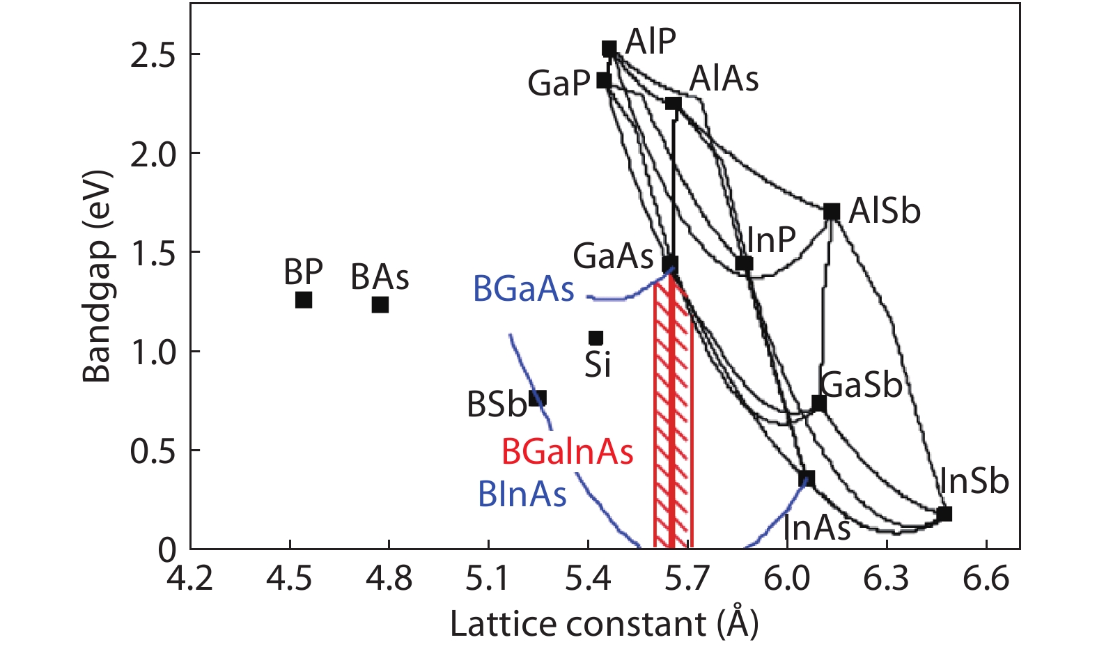
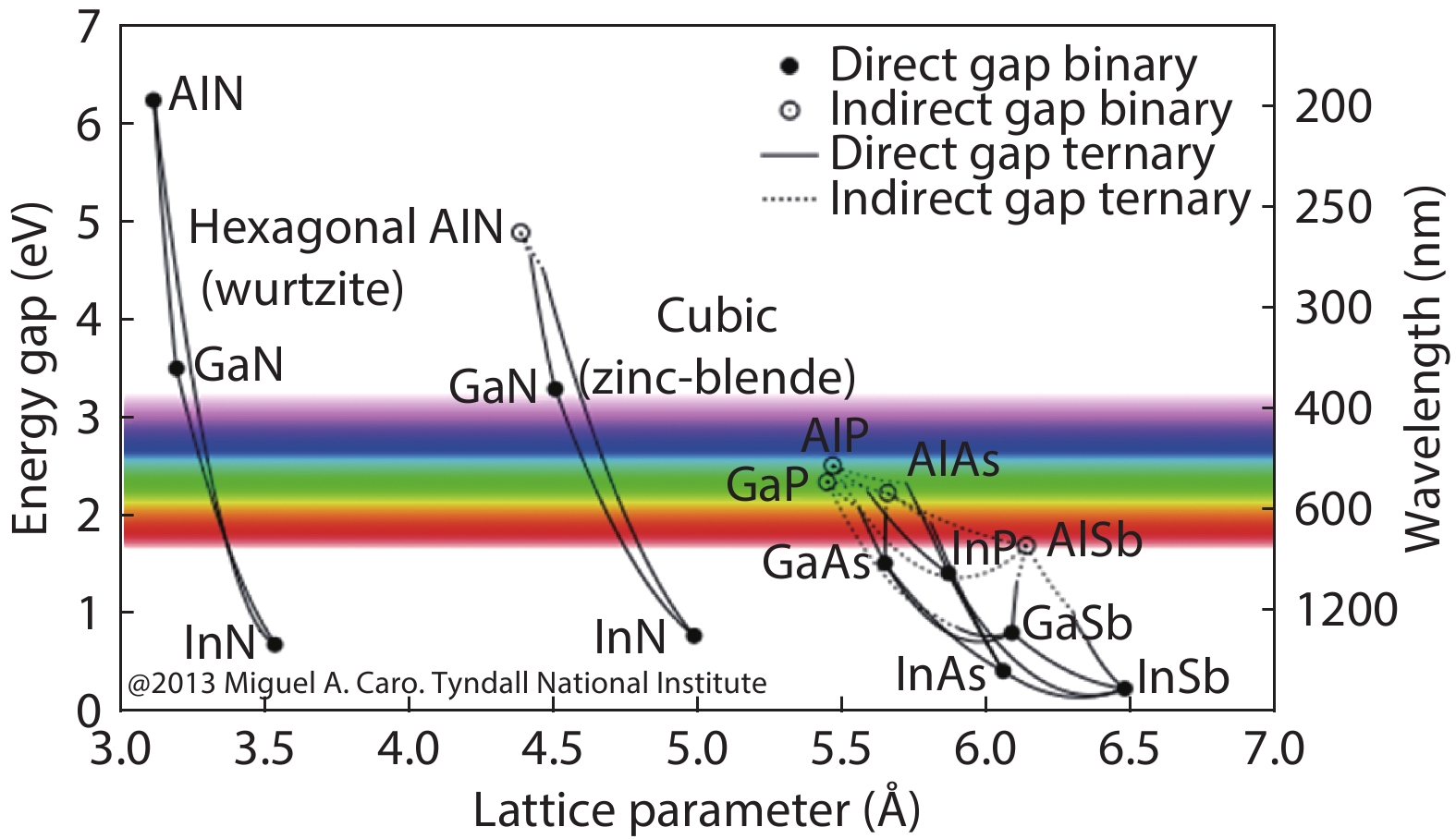
Compared to their antecessor Si, III–V compound semiconductors have versatile properties such as direct bandgap, higher carrier mobility, and smaller electron effective mass, making them highly attractive for microelectronic and optoelectronic applications in solid-state lighting, wireless communication, artificial intelligence, high-speed train, clean energy generation, and radar systems[58]. Fig. 1 shows the energy bandgap of III–V semiconductors as a function of their lattice parameters[9]. The materials have either zinc-blende or wurtzite crystal structures, most of which with direct bandgap. The wurtzite III-nitrides have bandgap value from 0.7 to 6.0 eV, while the zinc-blende arsenides from 0.35 to 2.24 eV, which covers a wide range of the electromagnetic spectrum.

Figure  1.  (Color online) The bandgap energy versus lattice constant of the III–V semiconductor material system. Reproduced with permission from Ref. [10]. Copyright 2013, Miguel ángel Caro Bayo.

The natural solution is to integrate III–V lasers on Si substrates by heterogeneous or monolithic ways. In heterogeneous integration, the III–V laser is wafer bonded to a Si substrate. The heat dissipation problem may deteriorate the device performance. John Bower et al. from the University of California, Santa Barbara demonstrated the on-chip and inter-chip optical interconnects using light-emitting devices bonded onto silicon substrates[11]. While for monolithic integration, III–V optoelectronic devices were grown on the Si substrate directly. However, it faces the challenge of lattice mismatch, thermal mismatch, and antiphase formation when growing III–V on Si. Liu et al. demonstrated high-performance quantum dot lasers directly grown on silicon substrates by using a nucleation layer and dislocation filter layers to reduce threading dislocations in the III–V epilayers[12].

Besides light emitters, a photodetector, especially in the infrared range on Si, will enable widespread applications on military action, artificial intelligence, and so on. A wafer-scale fabrication process will lead to the large-area photodetector, which also makes it affordable. Although silicon itself is an efficient photodetector, it can only cover up to ~1.1 μm. III–V materials grown by metamorphic approaches lead to excessive dark currents. Therefore, a lattice-matching way of growing III–V materials on Si is needed.

In the early days, boron was introduced to remove the defect states in AlGaAs. In 1992, B-doped (Al, Ga)As was investigated by Tischler from IBM T. J. Watson Research Center to study the possibility to eliminate the DX centers in (Al, Ga)As[13], which was common when the Al composition exceed 20%. Since the DX centers are originated from the lattice distortion after Si doping for n-type (Al, Ga)As, the introduction of B was expected to mitigate the distortion effect. However, except for the reduction in growth rate and increase in AlAs mole fraction, the incorporation of boron was not found leading to the elimination of DX centers.

Furthermore, the BGaInAs alloy was found can be tuned to be lattice-matched to GaAs and Si with a bandgap smaller than GaAs[14]. Although the attractive properties of B-doped III–V compounds, these materials did not attract much attention, mainly due to the difficulties in growth. It is challenging to increase the boron content in BGaInAs alloys due to the large miscibility gap of the BAs–Ga(In)As system and complicated kinetics of boron incorporation[14, 15]. In addition, boron arsenide has two different forms: B12As with rhombohedral structure, and BAs with zinc blended structure, which is needed for BGaAs growth[16, 17], and was also studied more intensively due to the ultrahigh thermal conductivity[1820]. The boron antisite defects and its segregation to the surface for B12As2 formation, make it difficult to achieve high-quality boron-doped III–V semiconductors[21].

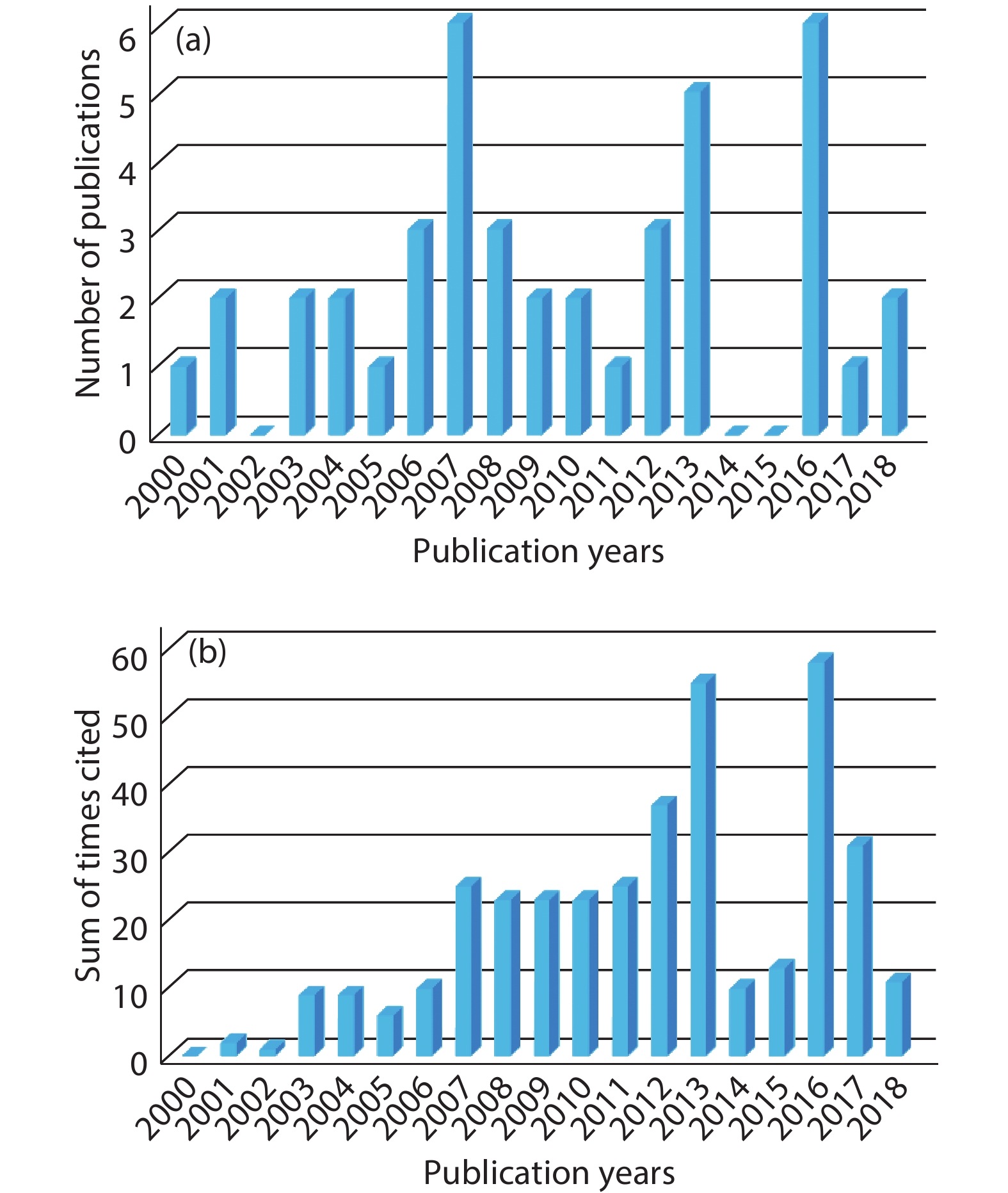
Because of the problems in the epitaxy such as B surface segregation, deteriorated surface, and B antisite formation, the research on B-doped III–V semiconductors is sparse[17, 22, 21]. Fig. 2 shows the number of publications per year and the sum of times cited per year from an ISI Web of Science search using the keywords “BGaAs”. These numbers show a slow development in this field. However, despite the difficulty of getting high-quality materials, their ability to be grown on silicon and GaAs substrates without mismatch strain, make it very attractive for next-generation optoelectronic and microelectronic devices.

Figure  2.  (Color online) (a) The number of publications and (b) times cited on BGaAs per year since 2000. Keyword: “BGaAs”. Web of Science search conducted: August 9, 2019.

Until now, we lack a useful review that appropriately summarizes the development, problems, and current situation of these boron-doped III–V semiconductors, along with their various applications. In this review, we focus on the epitaxy of BGaAs semiconductors and discuss the broad potential optoelectronic applications, including light emitters and photodetectors. The growth mechanisms, growth techniques, including metal-organic chemical vapor deposition (MOCVD) and molecular-beam epitaxy (MBE), and the optical properties of BGaAs are summarized in Section 2. In Section 3, we discuss different BGaAs compounds, investigating their characteristics and applications, followed by an elaboration on challenges and problems of boron-doped III–V semiconductors in Section 4. Finally, we give a summary and future perspectives of these materials in Section 5.

Since boron has highly different properties than other III and V elements, it is expected its incorporation into III–V semiconductors will induce a huge change in the properties of III–V semiconductors[23]. Because of the small covalent radius of boron atoms compared to gallium and indium, BAs has a zinc-blende structure with a reduced lattice constant of 4.77 Å and a bandgap of 1.46 eV[22, 24]. When boron atoms enter a GaAs lattice, they can go to either a gallium site or an arsenic site, which is determined by growth conditions. It was found that isovalent boron incorporation happened under As-rich conditions, which is preferred for BGaAs growth; on the other hand, boron atoms go to the arsenic site under Ga-rich conditions, leading to the formation of boron “antisite” defect where the boron acts as an acceptor[15].

Because of the lattice constant, BGaAs has been suggested as a strain-compensation barrier in InGaAs(N) system. Although there are still arguments on the bandgap variation of BGaAs with boron composition, it is clear it can be a replacement for InGaAs(N) in the infrared wavelength range when adding indium to the compounds[25]. Fig. 3 shows the bandgap of various boron-doped III–V semiconductors, and the boron incorporation may expand the range for bandgap engineering[26].

Figure  3.  (Color online) Calculated bandgap versus lattice-constant for III–V compounds including B-doped alloy. Reproduced with permission from Ref. [26]. Copyright 2019, OSA Publishing.

Similar to GaAs, BGaAs has been grown both by MOCVD and MBE. In the initial work, B-doped (Al, Ga)As was grown in a low-pressure metalorganic vapor phase epitaxy (MOVPE) system. In these systems, trimethylgallium (TMGa), trimethylaluminum (TMAl), and arsine (AsH3) were used as precursors for Ga, Al, and As. Diborane (B2H6) and trimethyl boron have been used as boron precursors[13]. In this way, Geisz et al. reported the first growth of BGaInAs alloys by MOCVD[27]. However, the parasitic reactions between precursors made it difficult to study the growth mechanism[25].

BGaAs was first grown by Hoke from Raytheon Research Division using MBE in 1993[16]. Because of the low vapor pressure of boron, a high-temperature source is necessary for an MBE system. However, the use of a PBN crucible leads to a measurable nitrogen background in the chamber, which incorporates into the BGaAs films. In MBE, the substrate temperature has to be optimized. At high temperature, the surface mobility of boron is enhanced, which leads to the formation of B–B bonds, the reduced substitutional B incorporation, and the crystal quality degradation. Differently, in V. K. Gupta’s system, a pyrolytic graphite liner inside a tungsten crucible was used for producing boron flux[17].

In this part, we will review the development and research progress of boron-doped III–V semiconductors from various groups. Since most groups reported the growth using MOCVD, we will introduce the progress in this field, then also cover MBE related growth and a few theoretical works.

The early study mainly focused on the growth conditions optimization and characterization of B(In)GaAs layers on GaAs substrates. In 2000, Geisz et al. from National Renewable Energy Laboratory reported the growth of BGaInAs alloys with boron concentration up to 4%, which has a lattice matched to GaAs[27]. Taking advantage of a small atom radius, boron has been used to offset the lattice expansion of InGaAs. With the same bandgap of 1.34 eV, the authors found the BxGa1–xyInyAs layer much less strained than the Ga1–xInyAs layer when both grown on GaAs. The bowing parameter of 4–8 meV/%B is close to other III–V alloy systems. These epilayers had specular morphology, and the boron composition was estimated from the peak splitting in the double-crystal X-ray diffraction (DCXRD), as shown in Fig. 4.

Figure  4.  Rocking curves of BGaAs and BxGa1–xyInyAs. Reproduced with permission from Ref. [27]. Copyright 2000, AIP Publishing.

To further improve the boron incorporation, the precursors used in MOCVD were studied systematically. In 2001, they first analyzed the boron incorporation into BxGa1–xAs using different Ga precursors (TEG and TMG) in MOCVD, although they behave differently, the incorporation efficiency and maximum achievable boron concentration both decrease when growth temperatures are higher than 600 °C[14]. It was later also found the incorporation at high temperatures could be recovered by using surfactants such as Bi[21], and a very high V/III ratio is needed to avoid the formation of B–B bonds in BxGa1–xAs. The kinetics, instead of thermodynamics of the growth play an essential factor in the boron incorporation, which is allowed in MOCVD and MBE process. Besides Ga precursors, the group also investigated the use of different boron precursors in MOVPE for BGaAs epitaxy in a separate work. It was found that it is possible to incorporate boron below 600 °C, above which the incorporation drop dramatically due to the nature of the gas-phase reaction. Although the boron composition was extended to 4%–7%, the immiscibility of GaAs and BAs inhibited further improvement[28].

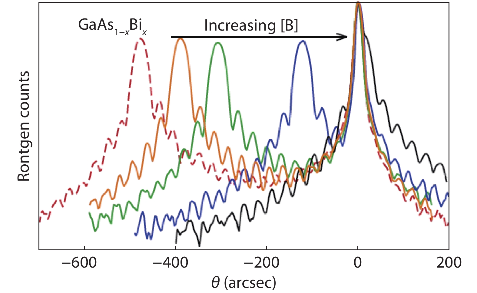
Bi has been used as a conventional surfactant in other material systems. To further improve the growth, the lab studied the growth of quaternary BGaAsBi lattice-matched to GaAs substrates in 2012[29]. Since bismuth is a large atom, co-doping with small boron atoms allows for strain compensation, which can be deduced from the XRD results in Fig. 5. The authors found the addition of boron atoms does not affect the bismuth incorporation, but if the boron amount in excess, antisite boron is incorporated, leading to an increase in hole density.

Figure  5.  (Color online) XRD rocking curves of the (004) peak for a GaAsBi ternary alloy and BGaAsBi alloy with different boron content. Reproduced with permission from Ref. [29]. Copyright 2012, Elsevier.

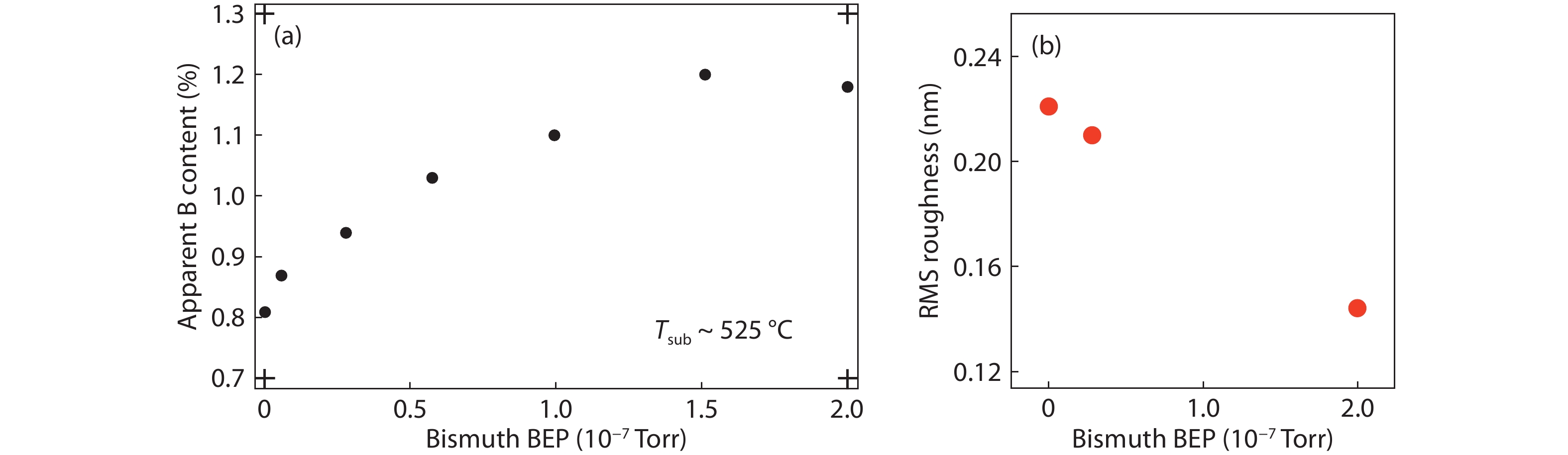
Similar to other reports, the amount of substitutional boron decreases with increasing substrate temperatures. However, the addition of a bismuth surfactant appears to force boron onto substitutional sites (see Fig. 6(a)), and makes the epilayers smoother (see Fig. 6(b))[30].

Figure  6.  (Color online) (a) Apparent boron concentration and (b) surface roughness versus Bi flux for samples. Reproduced with permission from Ref. [30]. Copyright 2012, Elsevier.

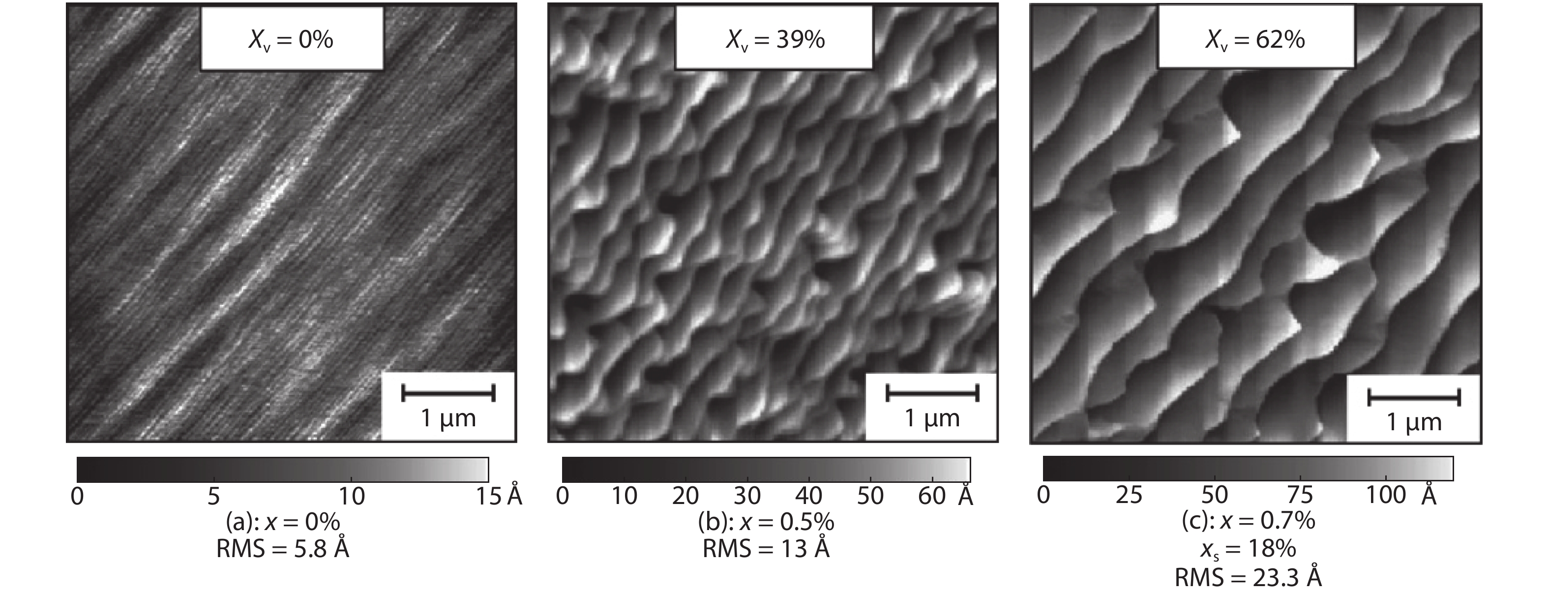
In 2003, H. Dumont from Université Claude Bernard Lyon 1 studied the growth of BGaAs on GaAs substrates[22, 25]. Similar to previous reports, the optimum temperature for boron incorporation is found to be 550–600 °C. The surface shows increasing surface roughnesses and a boron surface segregation, as shown in the atomic force microscopy (AFM) images in Fig. 7 and their X-ray photoelectron spectroscopy (XPS) results. The group later studied the thermodynamic conditions which determine the direction of the formation reaction of BGaAs. On the contrary, the kinetic conditions which determine formation conditions were not the focus of the study[31].

Figure  7.  AFM images of the surface with increasing boron content. Reproduced with permission from Refs. [17, 22]. Copyright 2003, AIP Publishing.

Besides surface morphology, the group also studied the optical properties of these BGaAs epilayers in 2004, which is necessary for their applications in optoelectronic devices. The temperature-dependent photoluminescence peak position showed an S-shaped behavior, which is a sign of the localized states due to nonuniform doping of boron atoms within the BGaAs epilayer. Similar behavior is also common in InGaAs layers grown on GaAs where indium segregation is observed. This is also verified by the large broadening of the BGaAs PL peak[32]. However, compared to dilute nitride GaNAs, it showed a reduced localization[33]. In 2009, they further investigated the boron incorporation in GaAs from the temperature-dependent PL measurements. A shift between theoretical fitting using Varshni law and experimental values was attributed to carriers trapped by localized states, which are mainly caused by the boron clustering in BGaAs[34, 35]. A similar phenomenon has also been observed in the BInGaAs system, as shown in Fig. 8(a)[36, 37].

Figure  8.  (a) Temperature dependence of PL peak energy of BGaAs epilayers. Reproduced with permission from Ref. [36]. Copyright 2010, Elsevier. (b) Low-temperature PL spectra of BInGaAs epilayer and quantum well. Reproduced with permission from Ref. [39]. Copyright 2012, Elsevier.

The group also investigated the BInGaAs single quantum well (SQW) grown by MOVPE[38, 39], as shown in Fig. 8(b). It is found the BInGaAs epilayer exhibits multiple PL peaks associated with the exciton bond induced by the boron clusters. In comparison, the PL of BInGaAs SQW only showed the interband transition influenced by the confinement of electron-hole pairs in the well.

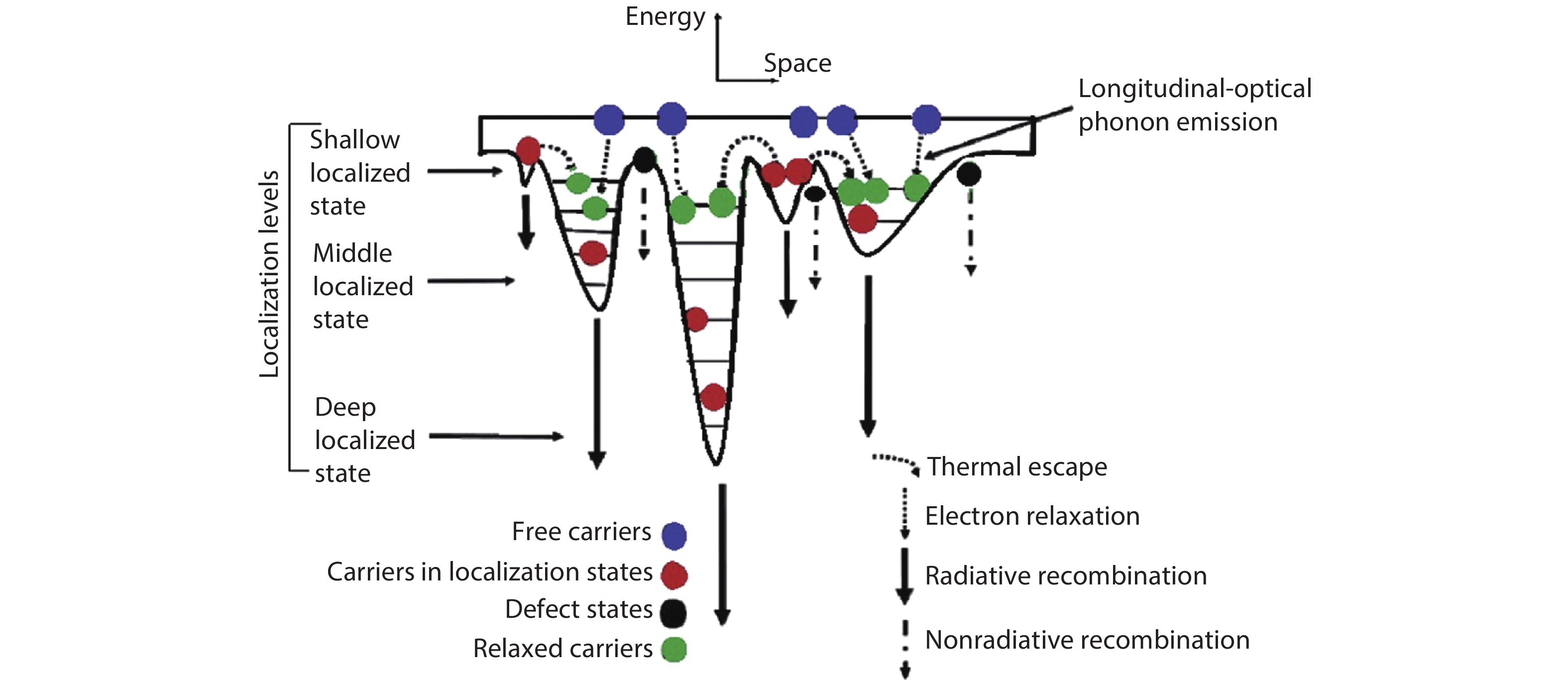
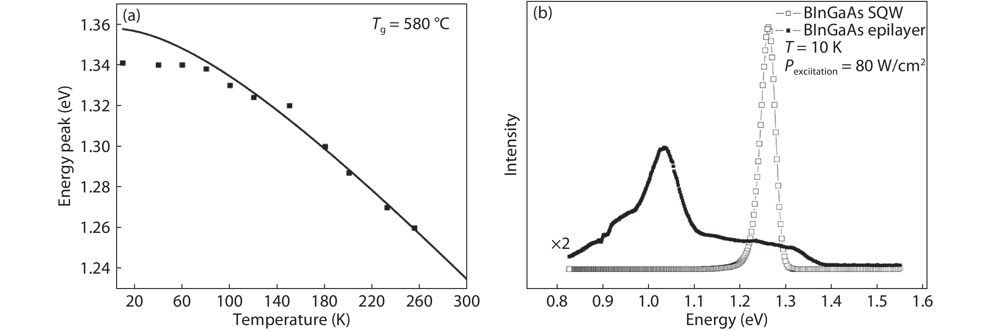
Furthermore, BInGaAs/GaAs quantum well with high indium composition was studied, it shows that a BInGaAs can be grown lattice-matched to GaAs as predicted. The temperature dependence of the PL peak energy showed an S-shaped behavior as a result of the competition process between localized and delocalized states of boron clusters. A model of carrier dynamics model was developed, as shown in Fig. 9. It explains the potential fluctuation caused by clusters, localized states, and possible paths for carrier transport and recombination in the material when the temperature increases[4043].

Figure  9.  (Color online) Schematic of spatial potential fluctuation and possible paths of carrier movement. Reproduced with permission from Ref. [41]. Copyright 2016, Elsevier.

Besides, the group also studied the influence of boron surface enrichment on the growth of BGaAs by MOVPE[44]. It was found the BGaAs step-bunching in Fig. 10 is related to the boron surface segregation with increasing diborane flow-rates during the MOVPE growth, which works as a surfactant to increase the surface mobility of Ga atoms.

Figure  10.  AFM images of 200 nm BGaAs/GaAs epilayers with various diborane flow-rates. Reproduced with permission from Ref. [44]. Copyright 2008, Elsevier.

Besides the AFM, PL characterization, photo-thermal deflection (PTD) technique was adopted to study the nonradiative recombination process in BGaAs/GaAs alloy in 2013. It was found with the increase of the boron composition, the induced localized states, clusters at BGaAs/GaAs interface, and roughness and imperfection of the surface change the transport properties of the BGaAs epilayer. Moreover, the thermal conductivity of BGaAs layers was found to decrease due to the allowing effects[4547].

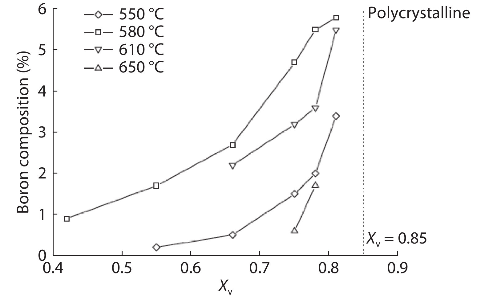
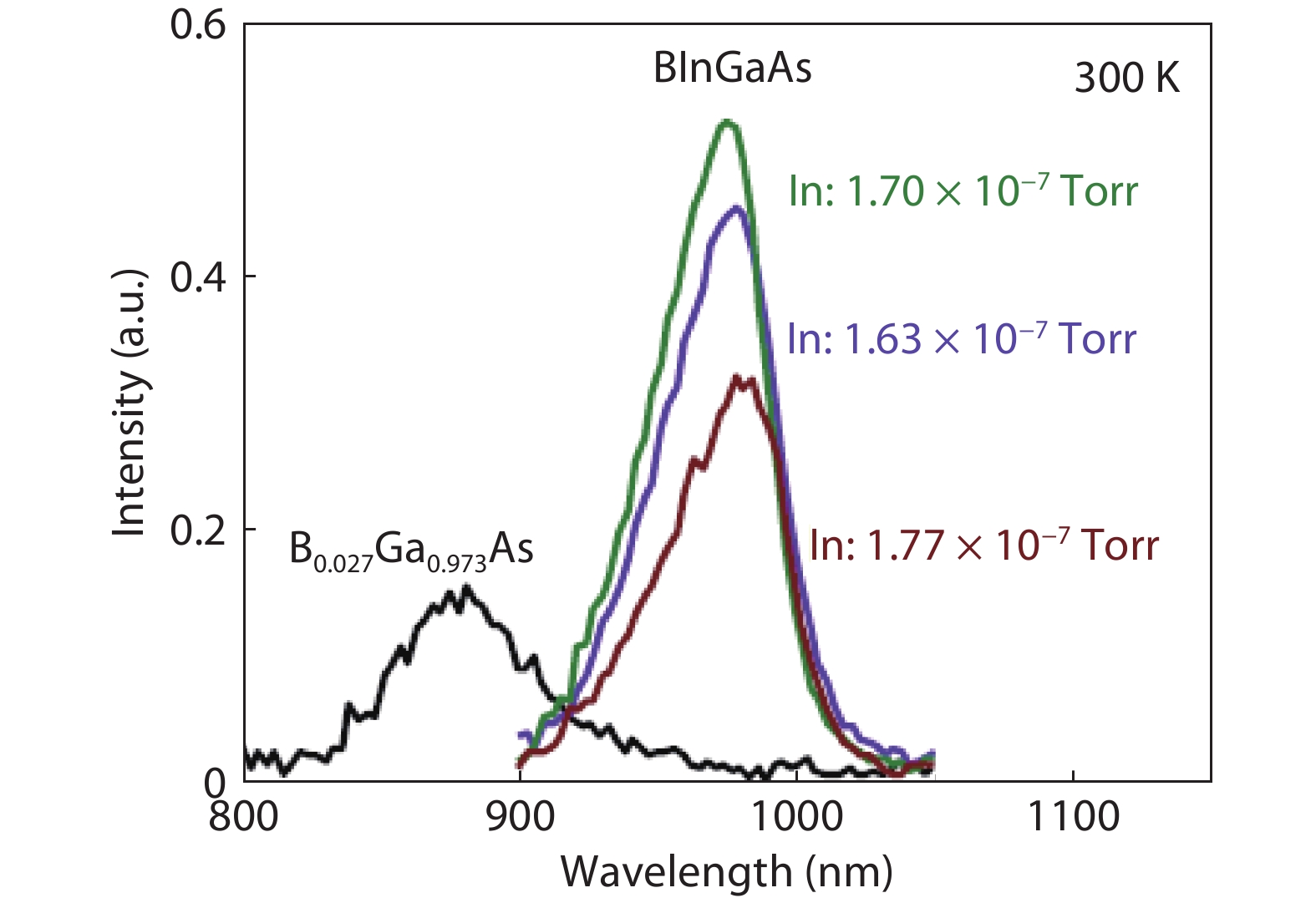
In 2008, Xiaomin Ren’s group from Beijing University of Posts and Telecommunications studied the growth of BGaAs on GaAs using LP-MOCVD[21, 48]. It was found that the boron incorporation decreases both at temperatures higher than 610 °C and temperatures lower than 550 °C. At the temperature from 550 to 610 °C, single-crystal films with specular surfaces could be grown when the boron concentration is within the range of 0.42–0.81, as shown in Fig. 11. At even higher temperatures, the boron-contained intermediate species may recombine or polymerize to the high molecular-weight species, which are difficult to be incorporated[49]. There is also a critical value for boron concentration, beyond which the polycrystalline or amorphous BGaAs with degraded surfaces formed. The group further demonstrated the growth of BAlAs and BGaInAs on GaAs substrates in 2009[49]. Low-temperature PL measurement of BGaInAs with boron composition of about 4% showed the emission wavelength of 1.24 μm.

Figure  11.  Boron composition of BGaAs as a function of boron concentration in the gas phase. Reproduced with permission from Ref. [50]. Copyright 2008, Elsevier.

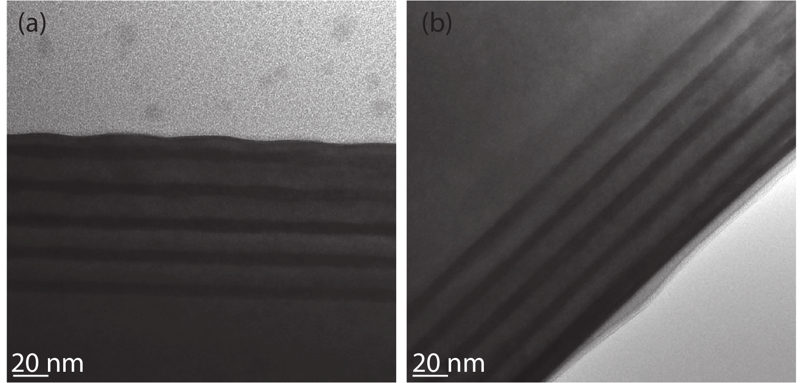
In 2013, the group further studied the effect of boron incorporation on the InGaAs/GaAs MQWs[34]. It was found when the strain is small, the boron incorporation will deteriorate the crystal quality. However, when the indium content in InGaAs/GaAs MQWs exceeds 40%, boron incorporation will help to reduce the compressive strain, leading to the flat surface, as shown in the transmission electron microscope (TEM) image in Fig. 12.

Figure  12.  Cross-sectional TEM images of (a) InGaAs/GaAs and (b) BInGaAs/GaAs. Reproduced with permission from Ref. [24]. Copyright 2013, AIP Publishing.

Compared to MOCVD, the study on BGaAs grown by MBE is relatively less. Gupta et al. from the University of Rochester reported BGaAs single crystal layer with boron composition up to 0.25% grown by MBE in 2000[17]. The layers showed a specular surface and p-type conductivity. The p-type conductivity was attributed due to the formation of boron antisites, which act as a double acceptor[51]. It was found that the low temperature will increase the boron incorporation in BGaAs. However, higher boron composition and higher growth temperature will both lead to the formation of boron-boron complexes, so the growth window for BGaAs is quite narrow.

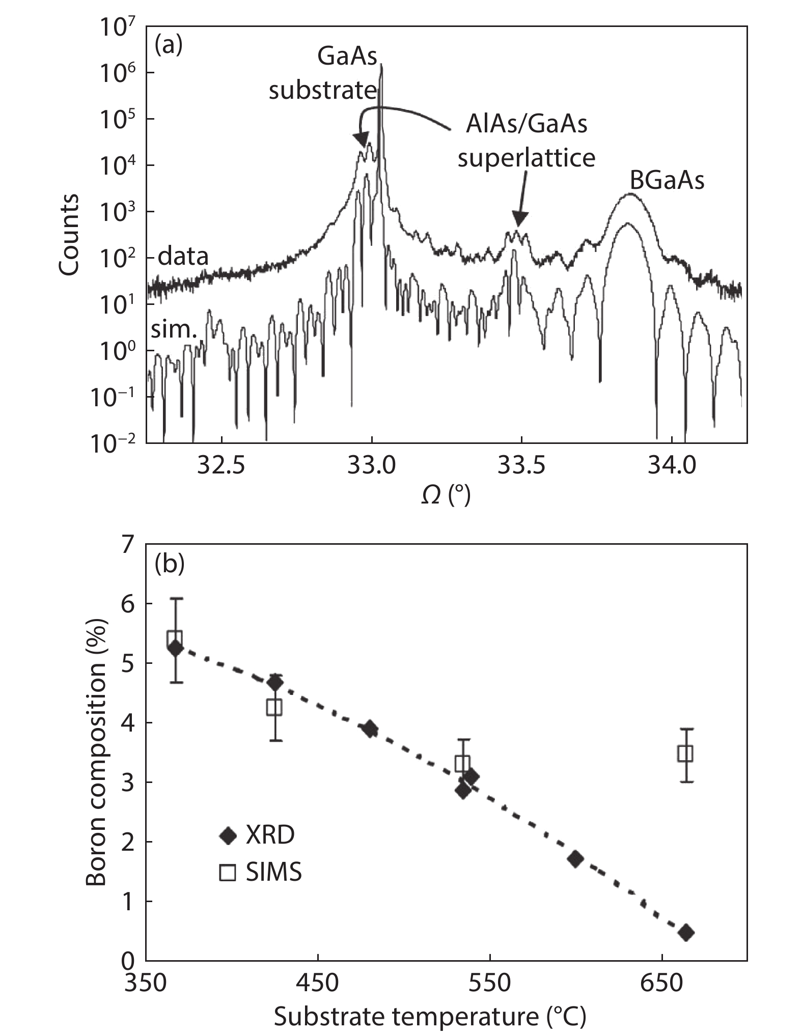
In 2004, Groenert from Infineon Technologies AG in Germany studied the growth of BGaAs by MBE, where the boron was provided by a high-temperature effusion cell. It was found that by reducing the growth temperature below 540 °C and increasing the V/III ratio above 20 it would improve the boron incorporation in the epitaxial layers; in the meantime, high temperature and low V/III ratio would lead to the B incorporation on interstitial lattice sites. The peak splitting in Fig. 13(a) was used to calculate the boron composition. As shown in the discrepancy of the boron composition at high temperature in Fig. 13(b), a large fraction of B atoms were not on Ga lattice sites at high temperatures. Because of the slow boron surface migration on GaAs and high cohesive energy of binary BAs compared to GaAs[52, 53], stationary boron atoms would be displaced into nearby interstitial sites by energetic highly mobile Ga atoms at high temperatures. Thus reducing Ga surface migration is the key to high boron content BGaAs formation. With the optimized condition, the B content of 7.8% was achieved[54].

Figure  13.  (a) X-ray rocking curve of a BGaAs ternary. (b) Boron composition as a function of substrate temperature. Reproduced with permission from Ref. [54]. Copyright 2004, Elsevier.

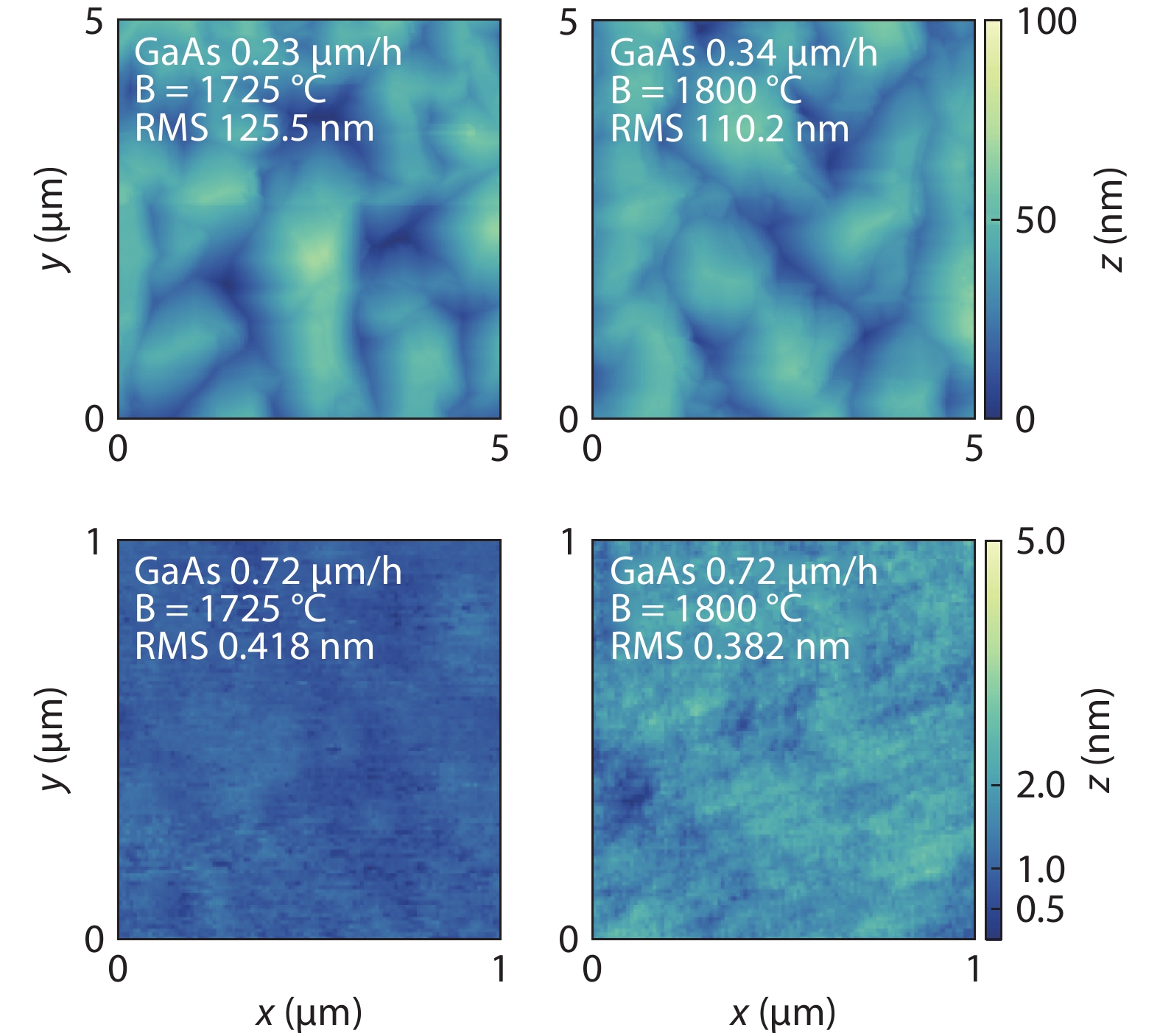
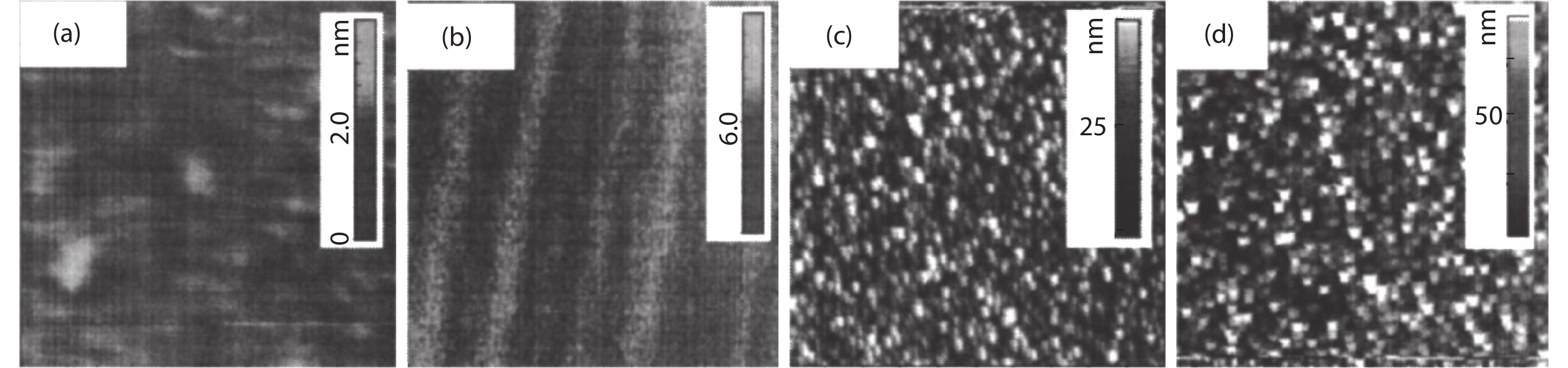
In 2017, Detz et al. from TU Wien studied the boron incorporation depending on the growth rate of GaAs. In their system, a pyrolytic graphite crucible operating at 1725–1800 °C was used for the boron source. It was found that a higher GaAs growth rate leads to a higher BAs growth rate[21]. Moreover, it is evident from the AFM images (see Fig. 14) that samples grown at high GaAs rates show a much smoother surface. The dependence of carrier concentration and mobility on the layer thickness indicates the formation of a different phase on the surface during the growth.

Figure  14.  (Color online) AFM images for BGaAs grown at different conditions. Reproduced with permission from Ref. [50]. Copyright 2017, Elsevier.

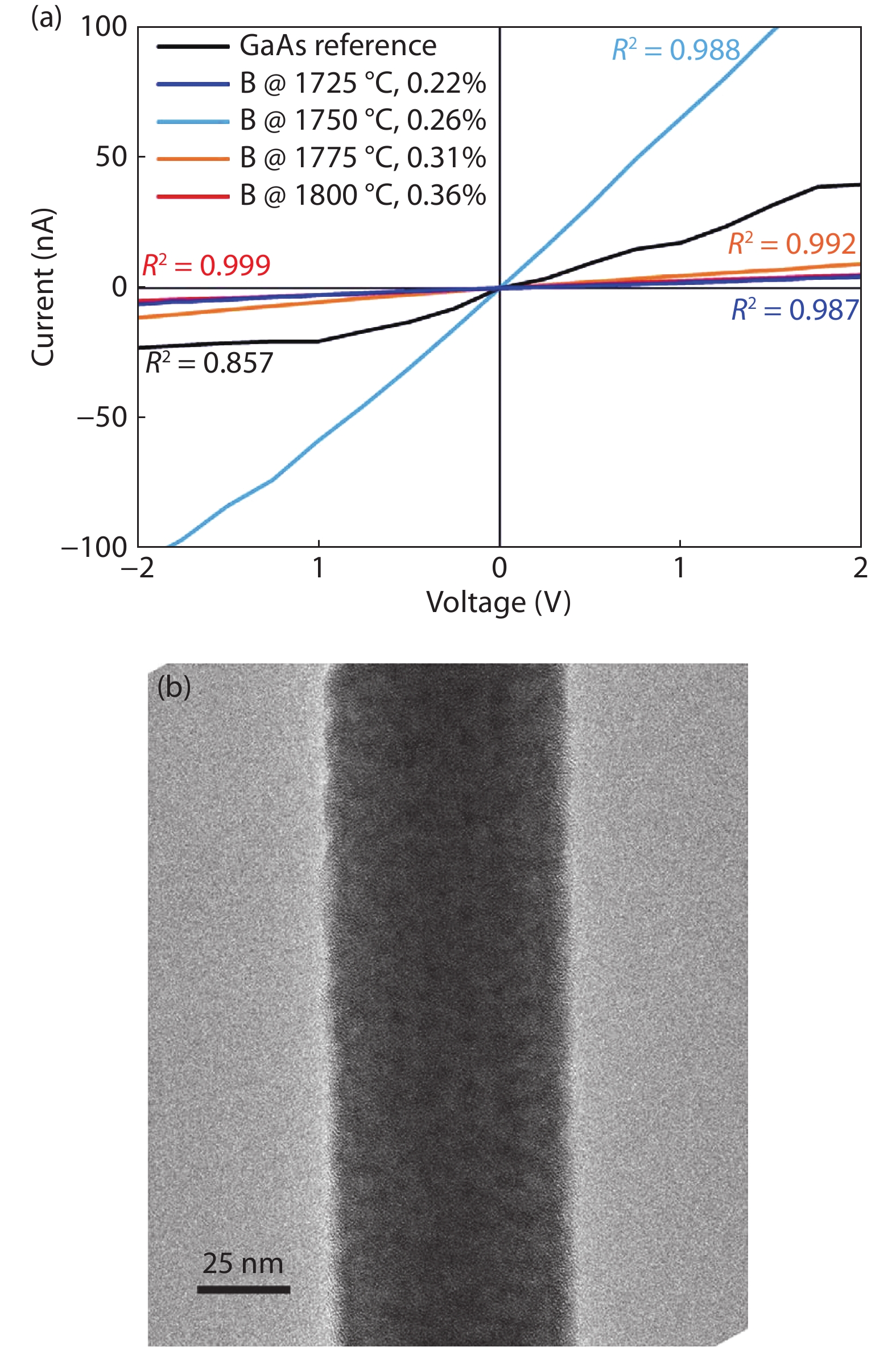
In 2019, Lancaster et al. from TU Wien also studied BGaAs but in the nanowire form. It was found that the surface segregation led to the high boron concentration at the edge. Its incorporation on antisites explains its p-type behavior[55]. As shown in the I–V curves for the samples in Fig. 15(a), the conductivity enhancement in boron-doped samples is attributed to the doping of and an increased contact surface area, as shown in Fig. 15(b). Moreover, because of the surfactant nature of B, it led to the reduced Ga adatom diffusion and consumption. Finally, the contact angle of Ga droplet changes and the crystal structures switch between zinc-blende and wurtzite, which leads to the formation of stacking faults in the nanowires[50].

Figure  15.  (Color online) (a) I–V measurements on nanowires with and without boron; (b) TEM image of nanowires. Reproduced with permission from Ref. [50]. Copyright 2019, John Wiley and Sons.

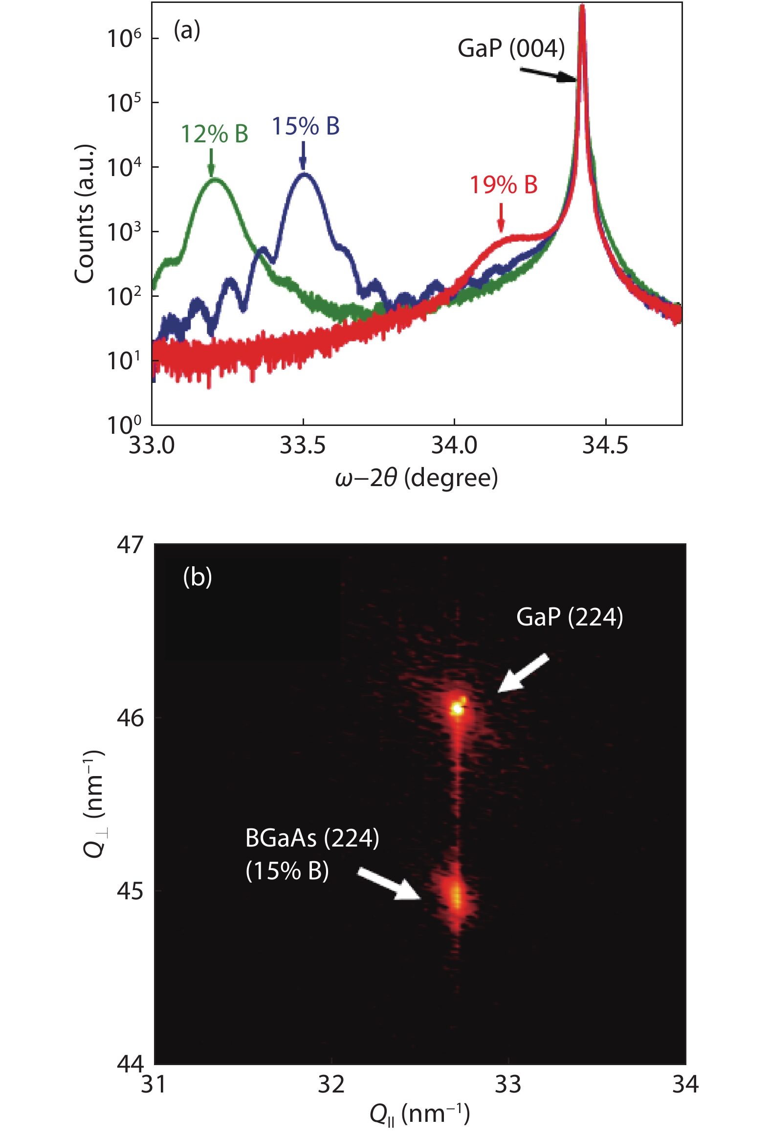
In 2018, Bank from the University of Texas at Austin reported exciting progress in this field. The growth of BGaAs on GaP using their high kinetically-limited growth regime with a high growth rate, a low substrate temperature, and using bismuth as a surfactant to limit surface diffusion of boron and showed promoted boron substitutional incorporation. The further increase of boron for lattice-matching BGaAs to GaP leads to the XRD peaks broadening and absence of fringes due to the phase segregation, as shown in Fig. 16. This happened because of the lack of a P-terminated surface during deoxidation and a GaP buffer layer to screen defects from the substrates[56]. After solving the problems, an improved interface indicated from the fringes in the XRD results and coherent film indicated from the reciprocal space mapping was demonstrated.

Figure  16.  (Color online) (a) ω–2θ scans of BGaAs films grown on a GaP buffer. (b) Reciprocal space mapping (RSM) of BGaAs layers grown on a GaP buffer. Reproduced with permission from Ref. [50]. Copyright 2018, IEEE.

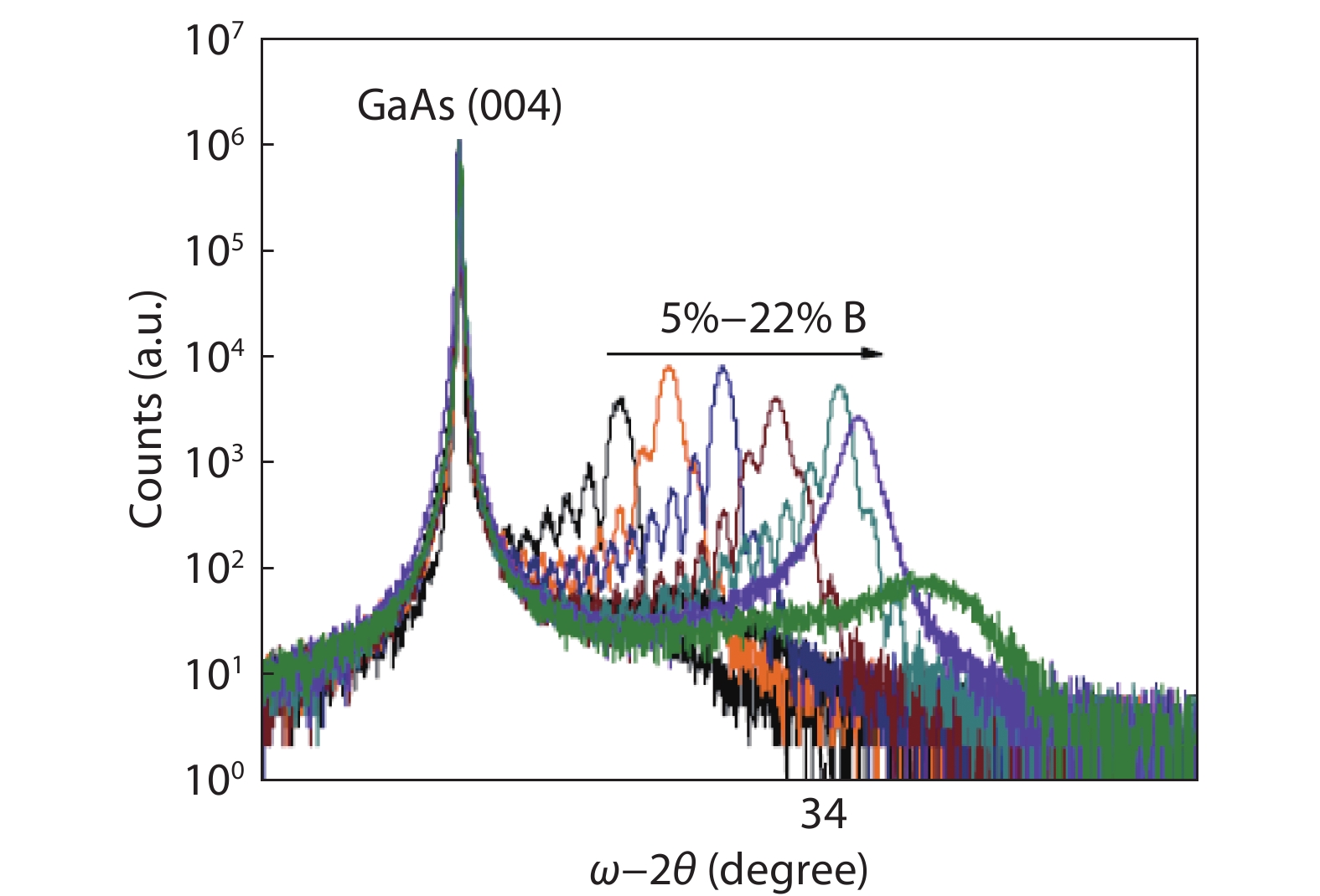
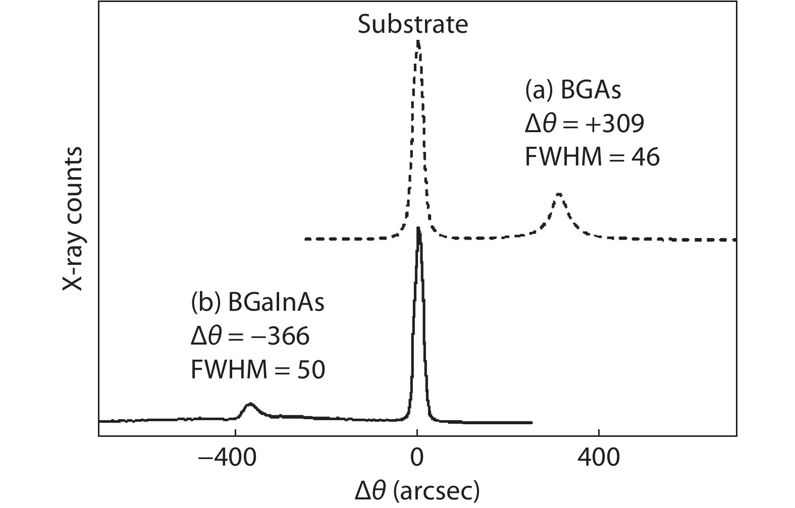
In 2019, Bank’s group further demonstrated 1.31 μm room temperature emission of BGaInAs alloy on GaAs substrates[26]. Since InGaAs QWs can not reach this wavelength range and the dilute nitride InGaAsN does not show the capability of reliable operation, this work opens a new route for laser structure epitaxy growth. Using their high kinetically-limited growth regime, substitutional incorporation of 12% boron is achieved, as shown in Fig. 17. The pendellösung fringes indicate the excellent quality of BGaAs/GaAs interface.

Figure  17.  (Color online) XRD of BGaAs films grown on GaAs substrates. Reproduced with permission from Ref. [26]. Copyright 2019, OSA Publishing.

To further extend the emission wavelength, indium was added into BGaAs alloy. Although BGaAs is a poor emitter due to the boron cluster states. The incorporation of indium atoms lowers the conduction band edge down to boron cluster states[26, 57], thus high internal quantum efficiency was achieved (see Fig. 18). The simultaneous incorporation of indium and boron broaden the wavelength range, which is very attractive for Si-based optoelectronic devices.

Figure  18.  (Color online) Room temperature photoluminescence of BGaAs and BGaInAs alloy. Reproduced with permission from Ref. [26]. Copyright 2019, OSA Publishing.

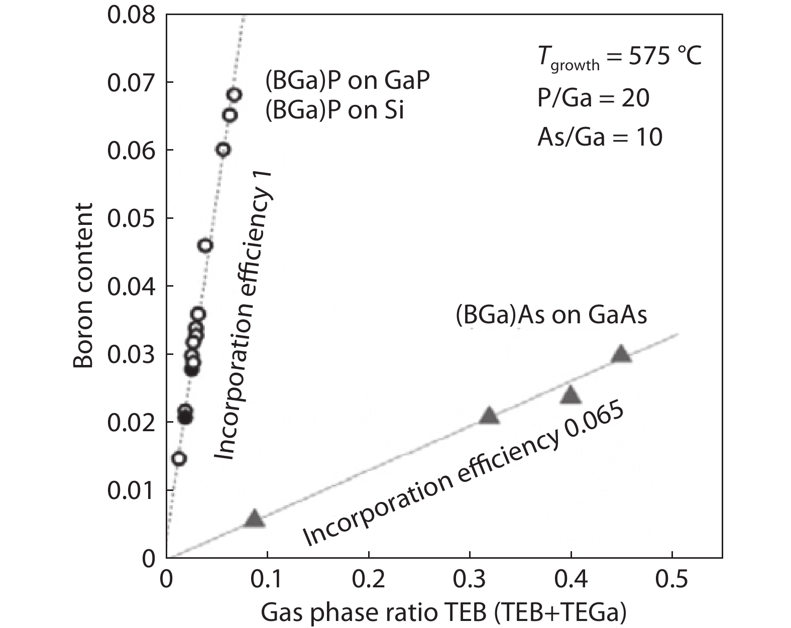
In comparison to boron-doped arsenides, Sommer et al. from Philipps-Universitat investigated the phosphorus-based materials doped with boron. The quaternary system (BGa)(AsP) was also discussed in their report[58]. Especially, the Ga(NAsP)/(BGa)(AsP)/(BGa)P material system is lattice-matched to Si substrate, thus is promising for Si-based microelectronics and optoelectronics. For boron-doped semiconductors, the phase separation into boron and gallium rich domains, together with the breakdown of the crystal structure due to small boron atoms induced local lattice distortions, limited the maximum boron doping concentration. As shown in Fig. 19, the boron incorporation efficiency in GaAs is only 6.5%, whereas it is 100% for GaP. Their work opened a new way for increasing boron incorporation in III–V semiconductors.

Figure  19.  Comparison of the boron concentration in GaP and GaAs. Reproduced with permission Ref. [50]. Copyright 2013, Elsevier.

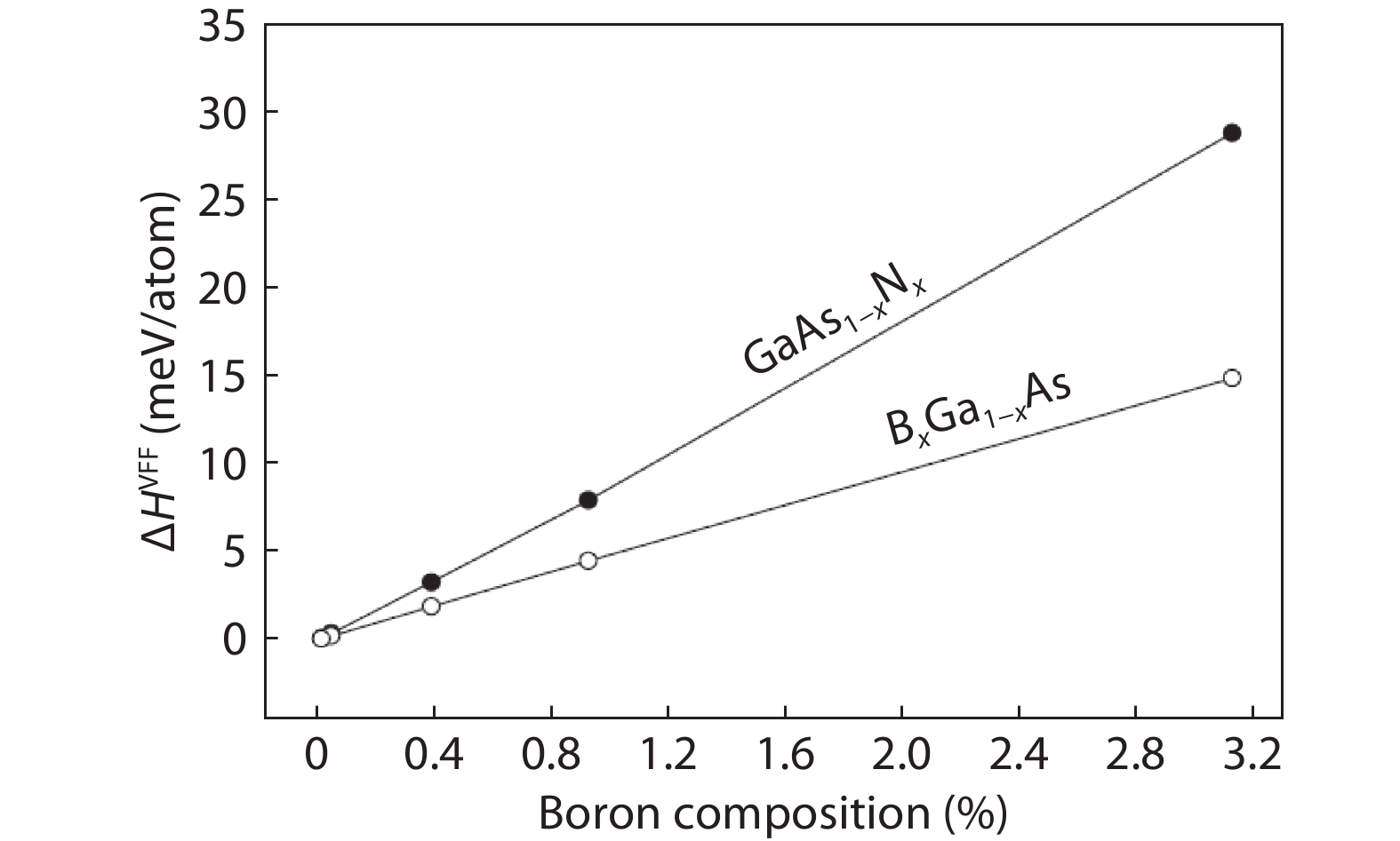
Besides experimental work, few theoretical works have been reported to predict and study the properties of these materials. The National Renewable Energy Laboratory also studied the electronic structure of boron-doped III–V semiconductor alloys[15]. It was found the band structure of BAs is closer to that of silicon than other III–V semiconductors. A smaller bandgap bowing of 3.5 eV for BxGa1−xAs compared to the well-studied GaAs1−xNx was predicted, and alloying GaAs with BAs leads to the increase of the bandgap. Moreover, the enthalpies of mixing BGaAs is lower than the GaAsN (see Fig. 20), which implies a larger composition range of BGaAs, especially for epitaxial layers[59].

Figure  20.  A comparison of calculated mixing enthalpies for GaAs1−xNx and BxGa1−xAs. Reproduced with permission from Ref. [59]. Copyright 2000, AIP Publishing.

Zaoui from Université des Sciences et de la Technologie de Lille studied the bandgap bowing of boron-doped III–V semiconductors[23]. By using a phenomenological model, they summarized the calculated total optical bandgap bowing btot, and its three physical contributions (volume deformation (VD), charge exchange (CE), and structural relaxation (SR)) in Table 1. The available theoretical (bthe) and measured values (bexp) are also listed as a comparison. It is suggested that the bowing of boron-doped III–V semiconductors are decided by strong competition between the three contributions.

Table  1.  Calculated bowing btot as well as its three contributions in eV. Reproduced with permission from Ref. [23]. Copyright 2007, Elsevier.
System bVD bCE bSR btot bthe bexp
Mixed cation
BAlN 4.88 1.62 –1.05 5.45
BGaN 7.47 1.47 –1.66 7.28 4.3 (x = 0.6)
BInN 14.73 2.03 –3.29 13.48
BAlP 4.41 1.20 –0.95 4.65
BGaP 4.61 1.04 –1.00 4.65
BInP 8.74 1.61 –1.92 8.43
BAlAs 2.77 1.17 –0.59 3.35
BGaAs 3.03 1.02 –0.66 3.39 3.5 (x < 0.6) 2.3 (x < 0.4)
BInAs 6.08 1.58 –1.34 6.32
BAlSb 0.15 1.07 –0.03 1.18
BGaSb –0.17 0.92 –0.09 0.65
BInSb 0.70 1.48 –0.08 2.10
Mixed anion
BNP 2.10 1.94 3.89 7.94 9.92
BNAs 5.13 2.29 4.87 12.30 9.33
BNSb 14.30 3.52 1.96 19.78 10.27, 21.19
BPSb 4.48 0.56 1.76 6.80 0.038
BPAs 0.52 0.34 0.00 0.87 –0.06
BAsSb 1.94 0.47 1.10 3.50 0.10
DownLoad: CSV  | Show Table

In 2007, Jenichen et al. from Leibniz-Institute for Surface Modification in Germany studied the stabilities and band gaps of B-doped III–V semiconductors using density-functional supercell calculations by considering the arrangement and composition of (B, In) atoms. It was found that in the case of boron antisite instead of isovalent substitution, the bandgap would strongly reduce[60]. Using the same method, the group also studied the surface substitution of (B, In) atoms[61]. It was found the isovalent incorporation of boron is possible under arsenic-rich and less boron exposure conditions, which agrees with previous experimental results. Moreover, they predicted it is energetically more stable to incorporate indium and boron together than to incorporate only one of them, which is exciting news for bandgap engineering of III–V semiconductors. Using density-functional theory, the reaction energies and barrier heights of precursors for MOCVD were calculated[62]. In 2008, Lindsay et al. from Tyndall National Institute in Ireland showed the B atoms have little effect on the bandgap of BGaAs. On the contrary, B pairs will introduce defect levels close to the edge of the conduction band[57].

Until now, different groups have reported the growth of boron-doped III–V semiconductors by MBE or MOCVD; the properties of the materials were also predicted by different theoretical groups. However, there are still many challenges to their development and applications. First, although researchers tried to improve the boron composition doped in these materials, it only reaches 12% on GaAs and 15.5% on GaP recently. A new growth regime is needed to increase the boron composition further and extend the wavelength range of BInGaAs, and make it more practical for infrared applications. Second, the bandgap theory and growth mechanism are still not clear; researchers reported contradictory results on these materials. Moreover, most of the works still focus on material characterization; the material quality is still not at a level ready for different optoelectronic devices. Until now, only very few device results from this material system was reported.

To summarize, we have reviewed the development of boron-doped III–V semiconductors, including different growth techniques such as MBE and MOCVD, the growth mechanism and their characterization, and few applications in optoelectronic devices. Although the first study was reported more than two decades ago, the materials remain undeveloped. To provide a better understanding of this field, we have detailed the progress from various groups, not only those who study the growth of materials but also who predict material properties theoretically, not only by MOCVD but also by MBE. We have further focused on their recent applications in optoelectronic devices such as lasers and detectors. However, it is necessary to further understand the boron doping behavior and extend the device application of boron-doped materials.

With further development in boron-doped III–V semiconductors, they will find practical applications in laser and detectors in the near- and mid-infrared range, not only on III–V substrates but also on large-scale, low-cost Si substrates. These devices will be essential for an optoelectronic integrated circuit. Moving forward, there is enormous potential for employing boron-doped III–V semiconductors in cross-disciplinary applications, such as autonomous vehicles, biomedical instrumentation, and tactical intelligence.


[1]
Janjua B, Ng T K, Zhao C, et al. True yellow light-emitting diodes as phosphor for tunable color-rendering index laser-based white light. ACS Photonics, 2016, 3, 2089 doi: 10.1021/acsphotonics.6b00457
[2]
Zhao C, Ng T K, Tseng C C, et al. InGaN/GaN nanowires epitaxy on large-area MoS2 for high-performance light-emitters. RSC Adv, 2017, 7, 26665 doi: 10.1039/C7RA03590J
[3]
Zhao C, Ebaid M, Zhang H, et al. Quantified hole concentration in AlGaN nanowires for high-performance ultraviolet emitters. Nanoscale, 2018, 10, 15980 doi: 10.1039/C8NR02615G
[4]
Zhao C, Alfaraj N, Subedi R C, et al. III-nitride nanowires on unconventional substrates: From materials to optoelectronic device applications. Prog Quantum Electron, 2018, 61, 1 doi: 10.1016/j.pquantelec.2018.07.001
[5]
Janjua B, Sun H, Zhao C, et al. Self-planarized quantum-disks-in-nanowires ultraviolet-B emitters utilizing pendeo-epitaxy. Nanoscale, 2017, 9, 7805 doi: 10.1039/C7NR00006E
[6]
Ebaid M, Priante D, Liu G, et al. Unbiased photocatalytic hydrogen generation from pure water on stable Ir-treated In0.33Ga0.67N nanorods. Nano Energy, 2017, 37, 158 doi: 10.1016/j.nanoen.2017.05.013
[7]
Zhao C, Chen Y H, Xu B, et al. Study of the wetting layer of InAs/GaAs nanorings grown by droplet epitaxy. Appl Phys Lett, 2008, 92, 063122 doi: 10.1063/1.2883931
[8]
Zhao C, Chen Y H, Xu B, et al. Evolution of InAs nanostructures grown by droplet epitaxy. Appl Phys Lett, 2007, 91, 033112 doi: 10.1063/1.2757151
[9]
Siddiqi G, Pan Z, Hu S. III–V semiconductor photoelectrodes. Semiconductors and Semimetals, 2017, 81
[10]
Caro Bayo M Á. Theory of elasticity and electric polarization effects in the group-III nitrides. PhD Dissertation, University College Cork, 2013
[11]
Roelkens G, Liu L, Liang D, et al. III–V/silicon photonics for on-chip and intra-chip optical interconnects. Laser Photonics Rev, 2010, 4, 751 doi: 10.1002/lpor.200900033
[12]
Chen S, Li W, Wu J, et al. Electrically pumped continuous-wave III–V quantum dot lasers on silicon. Nat Photonics, 2016, 10, 307 doi: 10.1038/nphoton.2016.21
[13]
Tischler M A, Mooney P M, Parker B D, et al. Metalorganic vapor phase epitaxy and characterization of boron-doped (Al,Ga)As. J Appl Phys, 1992, 71, 984 doi: 10.1063/1.351295
[14]
Geisz J F, Friedman D J, Kurtz S, et al. Epitaxial growth of BGaAs and BGaInAs by MOCVD. J Cryst Growth, 2001, 225, 372 doi: 10.1016/S0022-0248(01)00883-1
[15]
Hart G L W, Zunger A. Electronic structure of BAs and boride III–V alloys. Phys Rev B, 2000, 62, 13522 doi: 10.1103/PhysRevB.62.13522
[16]
Hoke W E. Molecular-beam epitaxial growth of boron-doped GaAs films. J Vac Sci Technol B, 1993, 11, 902 doi: 10.1116/1.586734
[17]
Gupta V K, Koch M W, Watkins N J, et al. Molecular beam epitaxial growth of BGaAs ternary compounds. J Electron Mater, 2000, 29, 1387 doi: 10.1007/s11664-000-0123-3
[18]
Tian F, Song B, Chen X, et al. Unusual high thermal conductivity in boron arsenide bulk crystals. Science, 2018, 361, 582 doi: 10.1126/science.aat7932
[19]
Li S, Zheng Q, Lv Y, et al. High thermal conductivity in cubic boron arsenide crystals. Science, 2018, 361, 579 doi: 10.1126/science.aat8982
[20]
Kang J S, Li M, Wu H, et al. Experimental observation of high thermal conductivity in boron arsenide. Science, 2018, 361, 575 doi: 10.1126/science.aat5522
[21]
Detz H, MacFarland D, Zederbauer T, et al. Growth rate dependence of boron incorporation into BxGa1− xAs layers. J Cryst Growth, 2017, 477, 77 doi: 10.1016/j.jcrysgro.2017.02.043
[22]
Dumont H, Rutzinger D, Vincent C, et al. Surface segregation of boron in BxGa1− xAs/GaAs epilayers studied by X-ray photoelectron spectroscopy and atomic force microscopy. Appl Phys Lett, 2003, 82, 1830 doi: 10.1063/1.1561164
[23]
Azzi S, Zaoui A, Ferhat M. On the importance of the band gap bowing in boron-based III–V ternary alloys. Solid State Commun, 2007, 144, 245 doi: 10.1016/j.ssc.2007.08.017
[24]
Pryakhin D A. Growth of BGaAs layers on GaAs substrates by metal–organic vapor-phase epitaxy. Semiconductors, 2005, 39, 11 doi: 10.1134/1.1852634
[25]
Dumont H, Dazord J, Monteil Y, et al. Growth and characterization of high quality BxGa1− xAs/GaAs(001) epilayers. J Cryst Growth, 2003, 248, 463 doi: 10.1016/S0022-0248(02)01822-5
[26]
El-Jaroudi R H, McNicholas K M, Bouslog B A, et al. Boron alloys for GaAs-based 1.3 μm semiconductor lasers. Conference on Lasers and Electro-Optics, 2019
[27]
Geisz J F, Friedman D J, Olson J M, et al. BGaInAs alloys lattice matched to GaAs. Appl Phys Lett, 2000, 76, 1443 doi: 10.1063/1.126058
[28]
Geisz J F, Friedman D J, Kurtz S, et al. Alternative boron precursors for BGaAs epitaxy. J Electron Mater, 2001, 30, 1387 doi: 10.1007/s11664-001-0188-7
[29]
Beaton D A, Ptak A J, Alberi K, et al. Quaternary bismide alloy lattice matched to GaAs. J Cryst Growth, 2012, 351, 37 doi: 10.1016/j.jcrysgro.2012.04.028
[30]
Ptak A J, Beaton D A, Mascarenhas A. Growth of BGaAs by molecular-beam epitaxy and the effects of a bismuth surfactant. J Cryst Growth, 2012, 351, 122 doi: 10.1016/j.jcrysgro.2012.04.026
[31]
Dumont H, Monteil Y. Some aspects on thermodynamic properties, phase diagram and alloy formation in the ternary system BAs–GaAs—Part II: BGaAs alloy formation. J Cryst Growth, 2006, 290, 419 doi: 10.1016/j.jcrysgro.2005.12.080
[32]
Saidi F, Hassen F, Maaref H, et al. Optical study of BxGa1− xAs/GaAs epilayers. Mater Sci Engi C, 2006, 26, 236 doi: 10.1016/j.msec.2005.10.056
[33]
Saidi F, Hassen F, Dumont H, et al. Comparative optical study of GaAs1− xNx/GaAs and BxGa1− xAs/GaAs epilayers. IEE Proc - Optoelectron, 2004, 151, 342 doi: 10.1049/ip-opt:20040938
[34]
Wang Q, Jia Z, Ren X, et al. Effect of boron incorporation on the structural and photoluminescence properties of highly-strained InxGa1− xAs/GaAs multiple quantum wells. AIP Adv, 2013, 3, 072111 doi: 10.1063/1.4815971
[35]
Hamila R, Saidi F, Fouzri A, et al. Clustering effects in optical properties of BGaAs/GaAs epilayers. J Lumin, 2009, 129, 1010 doi: 10.1016/j.jlumin.2009.04.013
[36]
Hamila R, Saidi F, Rodriguez P H, et al. Growth temperature effects on boron incorporation and optical properties of BGaAs/GaAs grown by MOCVD. J Alloys Compnd, 2010, 506, 10 doi: 10.1016/j.jallcom.2010.06.169
[37]
Saidi F, Hamila R, Maaref H, et al. Structural and optical study of BxInyGa1− x yAs/GaAs and InyGa1− yAs/GaAs QW’s grown by MOCVD. J Alloys Compnd, 2010, 491, 45 doi: 10.1016/j.jallcom.2009.10.244
[38]
Rodriguez P, Auvray L, Dumont H, et al. Growth and characterization of BGaAs and BInGaAs epilayers on GaAs by MOVPE. J Cryst Growth, 2007, 298, 81 doi: 10.1016/j.jcrysgro.2006.10.118
[39]
Hamila R, Saidi F, Maaref H, et al. Photoluminescence properties and high resolution X-ray diffraction investigation of BInGaAs/GaAs grown by the metalorganic vapour phase epitaxy method. J Appl Phys, 2012, 112, 063109 doi: 10.1063/1.4752031
[40]
Hamila R, Saidi F, Rodriguez P, et al. Structural and optical study of BInGaAs/GaAs quantum wells grown by MOVPE emitting above 1.1 eV. Microelectron Eng, 2016, 149, 5 doi: 10.1016/j.mee.2015.08.013
[41]
Hidouri T, Saidi F, Maaref H, et al. Localized state exciton model investigation of B-content effect on optical properties of BGaAs/GaAs epilayers grown by MOCVD. Vacuum, 2016, 132, 10 doi: 10.1016/j.vacuum.2016.07.018
[42]
Hidouri T, Saidi F, Maaref H, et al. LSE investigation of the thermal effect on band gap energy and thermodynamic parameters of BInGaAs/GaAs single quantum well. Opt Mater, 2016, 62, 267 doi: 10.1016/j.optmat.2016.10.010
[43]
Hidouri T, Saidi F, Maaref H, et al. Impact of photoluminescence temperature and growth parameter on the exciton localized in BxGa1-xAs/GaAs epilayers grown by MOCVD. Opt Mater, 2016, 60, 487 doi: 10.1016/j.optmat.2016.08.029
[44]
Rodriguez P, Auvray L, Favier A, et al. Influence of boron surface enrichment on the growth mode of BGaAs epilayers grown on GaAs by metalorganic vapour phase epitaxy. Thin Solid Films, 2008, 516, 8424 doi: 10.1016/j.tsf.2008.04.053
[45]
Ilahi S, Baira M, Saidi F, et al. Non-radiative recombination process in BGaAs/GaAs alloys: Two layer photothermal deflection model. J Alloys Compnd, 2013, 581, 358 doi: 10.1016/j.jallcom.2013.07.101
[46]
Ilahi S, Saidi F, Hamila R, et al. Photothermal deflection spectroscopy PDS investigation of optical and thermal properties of BGaAs/GaAs alloys. Curr Appl Phys, 2013, 13, 610 doi: 10.1016/j.cap.2012.11.002
[47]
Ilahi S, Saidi F, Hamila R, et al. Shift of the gap energy and thermal conductivity in BGaAs/GaAs alloys. Physica B, 2013, 421, 105 doi: 10.1016/j.physb.2013.03.045
[48]
Wang Q, Ren X, Wang F, et al. LP-MOCVD growth of ternary BxGa1− xAs epilayers on (001)GaAs substrates using TEB, TMGa and AsH3. Microelectron J, 2008, 39, 1678 doi: 10.1016/j.mejo.2008.02.017
[49]
Wang Q, Ren X, Huang H, et al. Growth of BxGa1− xAs, BxAl1− xAs and BxGa1− x yInyAs epilayers on (001) GaAs by low pressure metalorganic chemical vapor deposition. Microelectron J, 2009, 40, 87 doi: 10.1016/j.mejo.2008.06.066
[50]
Lancaster S, Groiss H, Zederbauer T, et al. Suppression of axial growth by boron incorporation in GaAs nanowires grown by self-catalyzed molecular beam epitaxy. Nanotechnology, 2019, 30, 065602 doi: 10.1088/1361-6528/aaf11e
[51]
Brierley S K, Hendriks H T, Hoke W E, et al. Observation of boron-related photoluminescence in GaAs layers grown by molecular beam epitaxy. Appl Phys Lett, 1993, 63, 812 doi: 10.1063/1.109916
[52]
Kley A, Ruggerone P, Scheffler M. Novel diffusion mechanism on the GaAs (001) surface: the role of adatom-dimer interaction. Phys Rev Letters, 1997, 79, 5278 doi: 10.1103/PhysRevLett.79.5278
[53]
Paulus B, Fulde P, Stoll H. Cohesive energies of cubic III-V semiconductors. Phys Rev B, 1996, 54, 2556 doi: 10.1103/PhysRevB.54.2556
[54]
Groenert M E, Averbeck R, Hösler W, et al. Optimized growth of BGaAs by molecular beam epitaxy. J Cryst Growth, 2004, 264, 123 doi: 10.1016/j.jcrysgro.2004.01.010
[55]
Lancaster S, Andrews A M, Stoeger-Pollach M, et al. Influence of boron antisite defects on the electrical properties of MBE-grown GaAs nanowires. Phys Status Solidi B, 2019, 256, 1800368 doi: 10.1002/pssb.201800368
[56]
Bank S R, McNicholas K M, El-Jaroudi R H, et al. Improved MWIR LED arrays on Si substrates for scene projectors. IEEE Research and Applications of Photonics In Defense Conference (RAPID), 2018
[57]
Lindsay A, O’Reilly E P. Theory of electronic structure of BGaAs and related alloys. Phys Status Solidi C, 2008, 5, 454 doi: 10.1002/pssc.200777456
[58]
Sommer N, Buss R, Ohlmann J, et al. Growth of (BGa)As, (BGa)P, (BGa)(AsP) and (BGaIn)P by MOVPE. J Cryst Growth, 2013, 370, 191 doi: 10.1016/j.jcrysgro.2012.07.035
[59]
Zhang S B, Zunger A. Surface-reconstruction-enhanced solubility of N, P, As, and Sb in III–V semiconductors. Appl Phys Lett, 1997, 71, 677 doi: 10.1063/1.119827
[60]
Jenichen A, Engler C. Stability and band gaps of InGaAs, BGaAs, and BInGaAs alloys: Density-functional supercell calculations. Phys Status Solidi B, 2007, 244, 1957 doi: 10.1002/pssb.200642215
[61]
Jenichen A, Engler C. Boron and indium substitution in GaAs (001) surfaces: Density-functional supercell calculations of the surface stability. Surf Sci, 2007, 601, 900 doi: 10.1016/j.susc.2006.11.043
[62]
Jenichen A, Engler C. Metalorganic chemical-vapour-deposition (MOCVD) of InGaAs, BGaAs, and BInGaAs: Quantum chemical calculations on the mechanisms. J Cryst Growth, 2007, 304, 26 doi: 10.1016/j.jcrysgro.2007.02.019
Fig. 1.  (Color online) The bandgap energy versus lattice constant of the III–V semiconductor material system. Reproduced with permission from Ref. [10]. Copyright 2013, Miguel ángel Caro Bayo.

Fig. 2.  (Color online) (a) The number of publications and (b) times cited on BGaAs per year since 2000. Keyword: “BGaAs”. Web of Science search conducted: August 9, 2019.

Fig. 3.  (Color online) Calculated bandgap versus lattice-constant for III–V compounds including B-doped alloy. Reproduced with permission from Ref. [26]. Copyright 2019, OSA Publishing.

Fig. 4.  Rocking curves of BGaAs and BxGa1–xyInyAs. Reproduced with permission from Ref. [27]. Copyright 2000, AIP Publishing.

Fig. 5.  (Color online) XRD rocking curves of the (004) peak for a GaAsBi ternary alloy and BGaAsBi alloy with different boron content. Reproduced with permission from Ref. [29]. Copyright 2012, Elsevier.

Fig. 6.  (Color online) (a) Apparent boron concentration and (b) surface roughness versus Bi flux for samples. Reproduced with permission from Ref. [30]. Copyright 2012, Elsevier.

Fig. 7.  AFM images of the surface with increasing boron content. Reproduced with permission from Refs. [17, 22]. Copyright 2003, AIP Publishing.

Fig. 8.  (a) Temperature dependence of PL peak energy of BGaAs epilayers. Reproduced with permission from Ref. [36]. Copyright 2010, Elsevier. (b) Low-temperature PL spectra of BInGaAs epilayer and quantum well. Reproduced with permission from Ref. [39]. Copyright 2012, Elsevier.

Fig. 9.  (Color online) Schematic of spatial potential fluctuation and possible paths of carrier movement. Reproduced with permission from Ref. [41]. Copyright 2016, Elsevier.

Fig. 10.  AFM images of 200 nm BGaAs/GaAs epilayers with various diborane flow-rates. Reproduced with permission from Ref. [44]. Copyright 2008, Elsevier.

Fig. 11.  Boron composition of BGaAs as a function of boron concentration in the gas phase. Reproduced with permission from Ref. [50]. Copyright 2008, Elsevier.

Fig. 12.  Cross-sectional TEM images of (a) InGaAs/GaAs and (b) BInGaAs/GaAs. Reproduced with permission from Ref. [24]. Copyright 2013, AIP Publishing.

Fig. 13.  (a) X-ray rocking curve of a BGaAs ternary. (b) Boron composition as a function of substrate temperature. Reproduced with permission from Ref. [54]. Copyright 2004, Elsevier.

Fig. 14.  (Color online) AFM images for BGaAs grown at different conditions. Reproduced with permission from Ref. [50]. Copyright 2017, Elsevier.

Fig. 15.  (Color online) (a) I–V measurements on nanowires with and without boron; (b) TEM image of nanowires. Reproduced with permission from Ref. [50]. Copyright 2019, John Wiley and Sons.

Fig. 16.  (Color online) (a) ω–2θ scans of BGaAs films grown on a GaP buffer. (b) Reciprocal space mapping (RSM) of BGaAs layers grown on a GaP buffer. Reproduced with permission from Ref. [50]. Copyright 2018, IEEE.

Fig. 17.  (Color online) XRD of BGaAs films grown on GaAs substrates. Reproduced with permission from Ref. [26]. Copyright 2019, OSA Publishing.

Fig. 18.  (Color online) Room temperature photoluminescence of BGaAs and BGaInAs alloy. Reproduced with permission from Ref. [26]. Copyright 2019, OSA Publishing.

Fig. 19.  Comparison of the boron concentration in GaP and GaAs. Reproduced with permission Ref. [50]. Copyright 2013, Elsevier.

Fig. 20.  A comparison of calculated mixing enthalpies for GaAs1−xNx and BxGa1−xAs. Reproduced with permission from Ref. [59]. Copyright 2000, AIP Publishing.

Table 1.   Calculated bowing btot as well as its three contributions in eV. Reproduced with permission from Ref. [23]. Copyright 2007, Elsevier.

System bVD bCE bSR btot bthe bexp
Mixed cation
BAlN 4.88 1.62 –1.05 5.45
BGaN 7.47 1.47 –1.66 7.28 4.3 (x = 0.6)
BInN 14.73 2.03 –3.29 13.48
BAlP 4.41 1.20 –0.95 4.65
BGaP 4.61 1.04 –1.00 4.65
BInP 8.74 1.61 –1.92 8.43
BAlAs 2.77 1.17 –0.59 3.35
BGaAs 3.03 1.02 –0.66 3.39 3.5 (x < 0.6) 2.3 (x < 0.4)
BInAs 6.08 1.58 –1.34 6.32
BAlSb 0.15 1.07 –0.03 1.18
BGaSb –0.17 0.92 –0.09 0.65
BInSb 0.70 1.48 –0.08 2.10
Mixed anion
BNP 2.10 1.94 3.89 7.94 9.92
BNAs 5.13 2.29 4.87 12.30 9.33
BNSb 14.30 3.52 1.96 19.78 10.27, 21.19
BPSb 4.48 0.56 1.76 6.80 0.038
BPAs 0.52 0.34 0.00 0.87 –0.06
BAsSb 1.94 0.47 1.10 3.50 0.10
DownLoad: CSV
[1]
Janjua B, Ng T K, Zhao C, et al. True yellow light-emitting diodes as phosphor for tunable color-rendering index laser-based white light. ACS Photonics, 2016, 3, 2089 doi: 10.1021/acsphotonics.6b00457
[2]
Zhao C, Ng T K, Tseng C C, et al. InGaN/GaN nanowires epitaxy on large-area MoS2 for high-performance light-emitters. RSC Adv, 2017, 7, 26665 doi: 10.1039/C7RA03590J
[3]
Zhao C, Ebaid M, Zhang H, et al. Quantified hole concentration in AlGaN nanowires for high-performance ultraviolet emitters. Nanoscale, 2018, 10, 15980 doi: 10.1039/C8NR02615G
[4]
Zhao C, Alfaraj N, Subedi R C, et al. III-nitride nanowires on unconventional substrates: From materials to optoelectronic device applications. Prog Quantum Electron, 2018, 61, 1 doi: 10.1016/j.pquantelec.2018.07.001
[5]
Janjua B, Sun H, Zhao C, et al. Self-planarized quantum-disks-in-nanowires ultraviolet-B emitters utilizing pendeo-epitaxy. Nanoscale, 2017, 9, 7805 doi: 10.1039/C7NR00006E
[6]
Ebaid M, Priante D, Liu G, et al. Unbiased photocatalytic hydrogen generation from pure water on stable Ir-treated In0.33Ga0.67N nanorods. Nano Energy, 2017, 37, 158 doi: 10.1016/j.nanoen.2017.05.013
[7]
Zhao C, Chen Y H, Xu B, et al. Study of the wetting layer of InAs/GaAs nanorings grown by droplet epitaxy. Appl Phys Lett, 2008, 92, 063122 doi: 10.1063/1.2883931
[8]
Zhao C, Chen Y H, Xu B, et al. Evolution of InAs nanostructures grown by droplet epitaxy. Appl Phys Lett, 2007, 91, 033112 doi: 10.1063/1.2757151
[9]
Siddiqi G, Pan Z, Hu S. III–V semiconductor photoelectrodes. Semiconductors and Semimetals, 2017, 81
[10]
Caro Bayo M Á. Theory of elasticity and electric polarization effects in the group-III nitrides. PhD Dissertation, University College Cork, 2013
[11]
Roelkens G, Liu L, Liang D, et al. III–V/silicon photonics for on-chip and intra-chip optical interconnects. Laser Photonics Rev, 2010, 4, 751 doi: 10.1002/lpor.200900033
[12]
Chen S, Li W, Wu J, et al. Electrically pumped continuous-wave III–V quantum dot lasers on silicon. Nat Photonics, 2016, 10, 307 doi: 10.1038/nphoton.2016.21
[13]
Tischler M A, Mooney P M, Parker B D, et al. Metalorganic vapor phase epitaxy and characterization of boron-doped (Al,Ga)As. J Appl Phys, 1992, 71, 984 doi: 10.1063/1.351295
[14]
Geisz J F, Friedman D J, Kurtz S, et al. Epitaxial growth of BGaAs and BGaInAs by MOCVD. J Cryst Growth, 2001, 225, 372 doi: 10.1016/S0022-0248(01)00883-1
[15]
Hart G L W, Zunger A. Electronic structure of BAs and boride III–V alloys. Phys Rev B, 2000, 62, 13522 doi: 10.1103/PhysRevB.62.13522
[16]
Hoke W E. Molecular-beam epitaxial growth of boron-doped GaAs films. J Vac Sci Technol B, 1993, 11, 902 doi: 10.1116/1.586734
[17]
Gupta V K, Koch M W, Watkins N J, et al. Molecular beam epitaxial growth of BGaAs ternary compounds. J Electron Mater, 2000, 29, 1387 doi: 10.1007/s11664-000-0123-3
[18]
Tian F, Song B, Chen X, et al. Unusual high thermal conductivity in boron arsenide bulk crystals. Science, 2018, 361, 582 doi: 10.1126/science.aat7932
[19]
Li S, Zheng Q, Lv Y, et al. High thermal conductivity in cubic boron arsenide crystals. Science, 2018, 361, 579 doi: 10.1126/science.aat8982
[20]
Kang J S, Li M, Wu H, et al. Experimental observation of high thermal conductivity in boron arsenide. Science, 2018, 361, 575 doi: 10.1126/science.aat5522
[21]
Detz H, MacFarland D, Zederbauer T, et al. Growth rate dependence of boron incorporation into BxGa1− xAs layers. J Cryst Growth, 2017, 477, 77 doi: 10.1016/j.jcrysgro.2017.02.043
[22]
Dumont H, Rutzinger D, Vincent C, et al. Surface segregation of boron in BxGa1− xAs/GaAs epilayers studied by X-ray photoelectron spectroscopy and atomic force microscopy. Appl Phys Lett, 2003, 82, 1830 doi: 10.1063/1.1561164
[23]
Azzi S, Zaoui A, Ferhat M. On the importance of the band gap bowing in boron-based III–V ternary alloys. Solid State Commun, 2007, 144, 245 doi: 10.1016/j.ssc.2007.08.017
[24]
Pryakhin D A. Growth of BGaAs layers on GaAs substrates by metal–organic vapor-phase epitaxy. Semiconductors, 2005, 39, 11 doi: 10.1134/1.1852634
[25]
Dumont H, Dazord J, Monteil Y, et al. Growth and characterization of high quality BxGa1− xAs/GaAs(001) epilayers. J Cryst Growth, 2003, 248, 463 doi: 10.1016/S0022-0248(02)01822-5
[26]
El-Jaroudi R H, McNicholas K M, Bouslog B A, et al. Boron alloys for GaAs-based 1.3 μm semiconductor lasers. Conference on Lasers and Electro-Optics, 2019
[27]
Geisz J F, Friedman D J, Olson J M, et al. BGaInAs alloys lattice matched to GaAs. Appl Phys Lett, 2000, 76, 1443 doi: 10.1063/1.126058
[28]
Geisz J F, Friedman D J, Kurtz S, et al. Alternative boron precursors for BGaAs epitaxy. J Electron Mater, 2001, 30, 1387 doi: 10.1007/s11664-001-0188-7
[29]
Beaton D A, Ptak A J, Alberi K, et al. Quaternary bismide alloy lattice matched to GaAs. J Cryst Growth, 2012, 351, 37 doi: 10.1016/j.jcrysgro.2012.04.028
[30]
Ptak A J, Beaton D A, Mascarenhas A. Growth of BGaAs by molecular-beam epitaxy and the effects of a bismuth surfactant. J Cryst Growth, 2012, 351, 122 doi: 10.1016/j.jcrysgro.2012.04.026
[31]
Dumont H, Monteil Y. Some aspects on thermodynamic properties, phase diagram and alloy formation in the ternary system BAs–GaAs—Part II: BGaAs alloy formation. J Cryst Growth, 2006, 290, 419 doi: 10.1016/j.jcrysgro.2005.12.080
[32]
Saidi F, Hassen F, Maaref H, et al. Optical study of BxGa1− xAs/GaAs epilayers. Mater Sci Engi C, 2006, 26, 236 doi: 10.1016/j.msec.2005.10.056
[33]
Saidi F, Hassen F, Dumont H, et al. Comparative optical study of GaAs1− xNx/GaAs and BxGa1− xAs/GaAs epilayers. IEE Proc - Optoelectron, 2004, 151, 342 doi: 10.1049/ip-opt:20040938
[34]
Wang Q, Jia Z, Ren X, et al. Effect of boron incorporation on the structural and photoluminescence properties of highly-strained InxGa1− xAs/GaAs multiple quantum wells. AIP Adv, 2013, 3, 072111 doi: 10.1063/1.4815971
[35]
Hamila R, Saidi F, Fouzri A, et al. Clustering effects in optical properties of BGaAs/GaAs epilayers. J Lumin, 2009, 129, 1010 doi: 10.1016/j.jlumin.2009.04.013
[36]
Hamila R, Saidi F, Rodriguez P H, et al. Growth temperature effects on boron incorporation and optical properties of BGaAs/GaAs grown by MOCVD. J Alloys Compnd, 2010, 506, 10 doi: 10.1016/j.jallcom.2010.06.169
[37]
Saidi F, Hamila R, Maaref H, et al. Structural and optical study of BxInyGa1− x yAs/GaAs and InyGa1− yAs/GaAs QW’s grown by MOCVD. J Alloys Compnd, 2010, 491, 45 doi: 10.1016/j.jallcom.2009.10.244
[38]
Rodriguez P, Auvray L, Dumont H, et al. Growth and characterization of BGaAs and BInGaAs epilayers on GaAs by MOVPE. J Cryst Growth, 2007, 298, 81 doi: 10.1016/j.jcrysgro.2006.10.118
[39]
Hamila R, Saidi F, Maaref H, et al. Photoluminescence properties and high resolution X-ray diffraction investigation of BInGaAs/GaAs grown by the metalorganic vapour phase epitaxy method. J Appl Phys, 2012, 112, 063109 doi: 10.1063/1.4752031
[40]
Hamila R, Saidi F, Rodriguez P, et al. Structural and optical study of BInGaAs/GaAs quantum wells grown by MOVPE emitting above 1.1 eV. Microelectron Eng, 2016, 149, 5 doi: 10.1016/j.mee.2015.08.013
[41]
Hidouri T, Saidi F, Maaref H, et al. Localized state exciton model investigation of B-content effect on optical properties of BGaAs/GaAs epilayers grown by MOCVD. Vacuum, 2016, 132, 10 doi: 10.1016/j.vacuum.2016.07.018
[42]
Hidouri T, Saidi F, Maaref H, et al. LSE investigation of the thermal effect on band gap energy and thermodynamic parameters of BInGaAs/GaAs single quantum well. Opt Mater, 2016, 62, 267 doi: 10.1016/j.optmat.2016.10.010
[43]
Hidouri T, Saidi F, Maaref H, et al. Impact of photoluminescence temperature and growth parameter on the exciton localized in BxGa1-xAs/GaAs epilayers grown by MOCVD. Opt Mater, 2016, 60, 487 doi: 10.1016/j.optmat.2016.08.029
[44]
Rodriguez P, Auvray L, Favier A, et al. Influence of boron surface enrichment on the growth mode of BGaAs epilayers grown on GaAs by metalorganic vapour phase epitaxy. Thin Solid Films, 2008, 516, 8424 doi: 10.1016/j.tsf.2008.04.053
[45]
Ilahi S, Baira M, Saidi F, et al. Non-radiative recombination process in BGaAs/GaAs alloys: Two layer photothermal deflection model. J Alloys Compnd, 2013, 581, 358 doi: 10.1016/j.jallcom.2013.07.101
[46]
Ilahi S, Saidi F, Hamila R, et al. Photothermal deflection spectroscopy PDS investigation of optical and thermal properties of BGaAs/GaAs alloys. Curr Appl Phys, 2013, 13, 610 doi: 10.1016/j.cap.2012.11.002
[47]
Ilahi S, Saidi F, Hamila R, et al. Shift of the gap energy and thermal conductivity in BGaAs/GaAs alloys. Physica B, 2013, 421, 105 doi: 10.1016/j.physb.2013.03.045
[48]
Wang Q, Ren X, Wang F, et al. LP-MOCVD growth of ternary BxGa1− xAs epilayers on (001)GaAs substrates using TEB, TMGa and AsH3. Microelectron J, 2008, 39, 1678 doi: 10.1016/j.mejo.2008.02.017
[49]
Wang Q, Ren X, Huang H, et al. Growth of BxGa1− xAs, BxAl1− xAs and BxGa1− x yInyAs epilayers on (001) GaAs by low pressure metalorganic chemical vapor deposition. Microelectron J, 2009, 40, 87 doi: 10.1016/j.mejo.2008.06.066
[50]
Lancaster S, Groiss H, Zederbauer T, et al. Suppression of axial growth by boron incorporation in GaAs nanowires grown by self-catalyzed molecular beam epitaxy. Nanotechnology, 2019, 30, 065602 doi: 10.1088/1361-6528/aaf11e
[51]
Brierley S K, Hendriks H T, Hoke W E, et al. Observation of boron-related photoluminescence in GaAs layers grown by molecular beam epitaxy. Appl Phys Lett, 1993, 63, 812 doi: 10.1063/1.109916
[52]
Kley A, Ruggerone P, Scheffler M. Novel diffusion mechanism on the GaAs (001) surface: the role of adatom-dimer interaction. Phys Rev Letters, 1997, 79, 5278 doi: 10.1103/PhysRevLett.79.5278
[53]
Paulus B, Fulde P, Stoll H. Cohesive energies of cubic III-V semiconductors. Phys Rev B, 1996, 54, 2556 doi: 10.1103/PhysRevB.54.2556
[54]
Groenert M E, Averbeck R, Hösler W, et al. Optimized growth of BGaAs by molecular beam epitaxy. J Cryst Growth, 2004, 264, 123 doi: 10.1016/j.jcrysgro.2004.01.010
[55]
Lancaster S, Andrews A M, Stoeger-Pollach M, et al. Influence of boron antisite defects on the electrical properties of MBE-grown GaAs nanowires. Phys Status Solidi B, 2019, 256, 1800368 doi: 10.1002/pssb.201800368
[56]
Bank S R, McNicholas K M, El-Jaroudi R H, et al. Improved MWIR LED arrays on Si substrates for scene projectors. IEEE Research and Applications of Photonics In Defense Conference (RAPID), 2018
[57]
Lindsay A, O’Reilly E P. Theory of electronic structure of BGaAs and related alloys. Phys Status Solidi C, 2008, 5, 454 doi: 10.1002/pssc.200777456
[58]
Sommer N, Buss R, Ohlmann J, et al. Growth of (BGa)As, (BGa)P, (BGa)(AsP) and (BGaIn)P by MOVPE. J Cryst Growth, 2013, 370, 191 doi: 10.1016/j.jcrysgro.2012.07.035
[59]
Zhang S B, Zunger A. Surface-reconstruction-enhanced solubility of N, P, As, and Sb in III–V semiconductors. Appl Phys Lett, 1997, 71, 677 doi: 10.1063/1.119827
[60]
Jenichen A, Engler C. Stability and band gaps of InGaAs, BGaAs, and BInGaAs alloys: Density-functional supercell calculations. Phys Status Solidi B, 2007, 244, 1957 doi: 10.1002/pssb.200642215
[61]
Jenichen A, Engler C. Boron and indium substitution in GaAs (001) surfaces: Density-functional supercell calculations of the surface stability. Surf Sci, 2007, 601, 900 doi: 10.1016/j.susc.2006.11.043
[62]
Jenichen A, Engler C. Metalorganic chemical-vapour-deposition (MOCVD) of InGaAs, BGaAs, and BInGaAs: Quantum chemical calculations on the mechanisms. J Cryst Growth, 2007, 304, 26 doi: 10.1016/j.jcrysgro.2007.02.019
1

Multiple SiGe/Si layers epitaxy and SiGe selective etching for vertically stacked DRAM

Zhenzhen Kong, Hongxiao Lin, Hailing Wang, Yanpeng Song, Junjie Li, et al.

Journal of Semiconductors, 2023, 44(12): 124101. doi: 10.1088/1674-4926/44/12/124101

2

Multilayered PdTe2/thin Si heterostructures as self-powered flexible photodetectors with heart rate monitoring ability

Chengyun Dong, Xiang An, Zhicheng Wu, Zhiguo Zhu, Chao Xie, et al.

Journal of Semiconductors, 2023, 44(11): 112001. doi: 10.1088/1674-4926/44/11/112001

3

Surface plasmon assisted high-performance photodetectors based on hybrid TiO2@GaOxNy-Ag heterostructure

Jiajia Tao, Guang Zeng, Xiaoxi Li, Yang Gu, Wenjun Liu, et al.

Journal of Semiconductors, 2023, 44(7): 072806. doi: 10.1088/1674-4926/44/7/072806

4

Epitaxial growth of CsPbBr3/PbS single-crystal film heterostructures for photodetection

Yifan Wang, Xuanze Li, Pei Liu, Jing Xia, Xiangmin Meng, et al.

Journal of Semiconductors, 2021, 42(11): 112001. doi: 10.1088/1674-4926/42/11/112001

5

Hydride vapor phase epitaxy for gallium nitride substrate

Jun Hu, Hongyuan Wei, Shaoyan Yang, Chengming Li, Huijie Li, et al.

Journal of Semiconductors, 2019, 40(10): 101801. doi: 10.1088/1674-4926/40/10/101801

6

Enhancement of photodetection based on perovskite/MoS2 hybrid thin film transistor

Fengjing Liu, Jiawei Wang, Liang Wang, Xiaoyong Cai, Chao Jiang, et al.

Journal of Semiconductors, 2017, 38(3): 034002. doi: 10.1088/1674-4926/38/3/034002

7

Strain effect on intersubband transitions in rolled-up quantum well infrared photodetectors

Han Wang, Shilong Li, Honglou Zhen, Xiaofei Nie, Gaoshan Huang, et al.

Journal of Semiconductors, 2017, 38(5): 054006. doi: 10.1088/1674-4926/38/5/054006

8

Research progress of Si-based germanium materials and devices

Buwen Cheng, Cheng Li, Zhi Liu, Chunlai Xue

Journal of Semiconductors, 2016, 37(8): 081001. doi: 10.1088/1674-4926/37/8/081001

9

Photodetectors based on two dimensional materials

Zheng Lou, Zhongzhu Liang, Guozhen Shen

Journal of Semiconductors, 2016, 37(9): 091001. doi: 10.1088/1674-4926/37/9/091001

10

Comment on Chen et al. "Fabrication and photovoltaic conversion enhancement of graphene/n-Si Schottky barrier solar cells by electrophoretic deposition", Electrochimica Acta, 2014

Lara Valentic, Nima E. Gorji

Journal of Semiconductors, 2015, 36(9): 094012. doi: 10.1088/1674-4926/36/9/094012

11

N+P photodetector characterization using the quasi-steady state photoconductance decay method

Omeime Xerviar Esebamen

Journal of Semiconductors, 2012, 33(12): 123002. doi: 10.1088/1674-4926/33/12/123002

12

Facile fabrication of UV photodetectors based on ZnO nanorod networks across trenched electrodes

Li Yingying, Cheng Chuanwei, Dong Xiang, Gao Junshan, Zhang Haiqian, et al.

Journal of Semiconductors, 2009, 30(6): 063004. doi: 10.1088/1674-4926/30/6/063004

13

Optical properties in 1D photonic crystal structure using Si/C60 multilayers

Chen Jing, Tang Jiyu, Han Peide, Chen Junfang

Journal of Semiconductors, 2009, 30(4): 043001. doi: 10.1088/1674-4926/30/4/043001

14

DCXRD Investigation of a Ge/Si(001) Island Multilayer Structure

Shi Wenhua, Xue Chunlai, Luo Liping, Wang Qiming

Chinese Journal of Semiconductors , 2007, 28(2): 145-148.

15

Impact of Transition-Metal Contamination on Oxygen Precipitation in Czochralski Silicon Under Rapid Thermal Processing

Wu Dongdong, Yang Deren, Xi Zhenqiang, Que Duanlin

Chinese Journal of Semiconductors , 2006, 27(3): 413-418.

16

Design and Simulation of Si-Based Resonant-Cavity-Enhanced Waveguide Photodetectors

Chen Liqun, Li Cheng

Chinese Journal of Semiconductors , 2006, 27(8): 1476-1479.

17

9μm Cutoff 128×128 AlGaAs/GaAs Quantum Well Infrared Photodetector Focal Plane Arrays

Li Xianjie, Liu Yingbin, Feng Zhen, Guo Fan, Zhao Yonglin, et al.

Chinese Journal of Semiconductors , 2006, 27(8): 1355-1359.

18

Rapid Thermal Annealing Characteristics of the Ge/Si(001)Nano-Island Multilayer

Shi Wenhua, Luo Liping, Zhao Lei, Zuo Yuhua, Wang Qiming, et al.

Chinese Journal of Semiconductors , 2006, 27(S1): 136-139.

19

Fabrication of 1.55μm Si-Based Resonant Cavity Enhanced Photodetectors

Mao Rongwei, Zuo Yuhua, Li Chuanbo, Cheng Buwen, Teng Xuegong, et al.

Chinese Journal of Semiconductors , 2005, 26(2): 271-275.

20

A GaAs-Based MOEMS Tunable RCE Photodetector with Single Cantilever Beam

Chinese Journal of Semiconductors , 2005, 26(6): 1087-1093.

1. Dubey, S.K., Nandi, S., Sravani, K.G. et al. Heterojunction concept and technology for FET developments. Field Effect Transistors, 2025. doi:10.1002/9781394248506.ch19
2. Abdullah, R., Jalil, A.A., Asmadi, M. et al. Recent advances in zinc oxide-based photoanodes for photoelectrochemical water splitting. International Journal of Hydrogen Energy, 2025. doi:10.1016/j.ijhydene.2024.05.461
3. Abdullah, R., Jalil, A.A., Asmadi, M. et al. Recent advances in zinc oxide-based photoanodes for photoelectrochemical water splitting. International Journal of Hydrogen Energy, 2025. doi:10.1016/j.ijhydene.2024.05.461
4. Fang, R., Zhou, S., Cao, W. et al. Research progress on irradiation effect of InP-based high electron mobility transistors | [磷化铟基高电子迁移率晶体管辐照效应研究现状]. He Jishu/Nuclear Techniques, 2025, 48(1): 010003. doi:10.11889/j.0253-3219.2025.hjs.48.230127
5. Luniov, S., Shygorin, P., Venhryn, B. THE INFLUENCE OF MECHANICAL STRAINS AND QUANTUM-SIZE EFFECTS ON THE PHOTOSENSITIVITY OF Ge/Ge(x)Si(1–x) NANOFILM. Romanian Journal of Physics, 2024, 69(1-2): 602. doi:10.59277/RomJPhys.2024.69.602
6. Zhang, Y., Zhou, T., Zhong, F. et al. Interfacial Effect on the Transient Dielectric Function and Charge Transfer in a Monolayer WS2/Si Heterojunction. ACS Applied Materials and Interfaces, 2023, 15(51): 59981-59988. doi:10.1021/acsami.3c16009
7. Chao, X., Yan, C., Zhao, H. et al. Micro-nano structural electrode architecture for high power energy storage. Journal of Semiconductors, 2023, 44(5): 050201. doi:10.1088/1674-4926/44/5/050201
8. He, S., Wang, Z., Wang, Z. et al. Recent progress and future prospect of novel multi-ion storage devices. Journal of Semiconductors, 2023, 44(4): 040201. doi:10.1088/1674-4926/44/4/040201
9. Nabi, S., Anwar, A.W., Wazir, Z. et al. First Principle Computation of Pure and (Sc, P, Bi)-Doped AlSb for Optoelectronic and Photonic Applications. Journal of Inorganic and Organometallic Polymers and Materials, 2023. doi:10.1007/s10904-023-02922-3
10. Wu, W., Wang, L., Shen, G. Flexible photoplethysmographic sensing devices for intelligent medical treatment. Journal of Materials Chemistry C, 2022, 11(1): 97-112. doi:10.1039/d2tc03318f
11. Hussein, S.S., Al-shatravi, A.G., Al-khursan, A.H. Optical absorption from boron-containing quantum dot structures. Micro and Nanostructures, 2022. doi:10.1016/j.micrna.2022.207375
12. Hu, Y., Qiu, C., Shen, T. et al. Direct calculations on the band offsets of large-lattice-mismatched and heterovalent Si and III–V semiconductors. Journal of Semiconductors, 2021, 42(11): 112102. doi:10.1088/1674-4926/42/11/112102
13. Liu, D., Tang, J., Meng, Y. et al. Ultra-low Vpp and high-modulation-depth InP-based electro-optic microring modulator. Journal of Semiconductors, 2021, 42(8): 082301. doi:10.1088/1674-4926/42/8/082301
14. Deshmukh, M.A., Park, S.-J., Hedau, B.S. et al. Recent progress in solar cells based on carbon nanomaterials. Solar Energy, 2021. doi:10.1016/j.solener.2021.04.001
15. Zhao, C., Li, Z., Tang, T. et al. Novel III-V semiconductor epitaxy for optoelectronic devices through two-dimensional materials. Progress in Quantum Electronics, 2021. doi:10.1016/j.pquantelec.2020.100313
16. He, Y., Lu, Z., Kuai, X. et al. Heterogeneous integration of InP and Si3N4 waveguides based on interlayer coupling for an integrated optical gyroscope. Applied Optics, 2021, 60(3): 662-669. doi:10.1364/AO.405799
17. Zhang, B.-T., Liu, H., Liu, Y. et al. Application trends of nanofibers in analytical chemistry. TrAC - Trends in Analytical Chemistry, 2020. doi:10.1016/j.trac.2020.115992
18. Ma, M., Huang, Y., Liu, J. et al. Engineering the photoelectrochemical behaviors of ZnO for efficient solar water splitting. Journal of Semiconductors, 2020, 41(9): 091702. doi:10.1088/1674-4926/41/9/091702
  • Search

    Advanced Search >>

    GET CITATION

    Chao Zhao, Bo Xu, Zhijie Wang, Zhanguo Wang. Boron-doped III–V semiconductors for Si-based optoelectronic devices[J]. Journal of Semiconductors, 2020, 41(1): 011301. doi: 10.1088/1674-4926/41/1/011301
    C Zhao, B Xu, Z J Wang, Z G Wang, Boron-doped III–V semiconductors for Si-based optoelectronic devices[J]. J. Semicond., 2020, 41(1): 011301. doi: 10.1088/1674-4926/41/1/011301.
    shu

    Export: BibTex EndNote

    Article Metrics

    Article views: 6027 Times PDF downloads: 261 Times Cited by: 18 Times

    History

    Received: 07 November 2019 Revised: Online: Accepted Manuscript: 06 December 2019Uncorrected proof: 13 December 2019Published: 02 January 2020

    Catalog

      Email This Article

      User name:
      Email:*请输入正确邮箱
      Code:*验证码错误
      Chao Zhao, Bo Xu, Zhijie Wang, Zhanguo Wang. Boron-doped III–V semiconductors for Si-based optoelectronic devices[J]. Journal of Semiconductors, 2020, 41(1): 011301. doi: 10.1088/1674-4926/41/1/011301 ****C Zhao, B Xu, Z J Wang, Z G Wang, Boron-doped III–V semiconductors for Si-based optoelectronic devices[J]. J. Semicond., 2020, 41(1): 011301. doi: 10.1088/1674-4926/41/1/011301.
      Citation:
      Chao Zhao, Bo Xu, Zhijie Wang, Zhanguo Wang. Boron-doped III–V semiconductors for Si-based optoelectronic devices[J]. Journal of Semiconductors, 2020, 41(1): 011301. doi: 10.1088/1674-4926/41/1/011301 ****
      C Zhao, B Xu, Z J Wang, Z G Wang, Boron-doped III–V semiconductors for Si-based optoelectronic devices[J]. J. Semicond., 2020, 41(1): 011301. doi: 10.1088/1674-4926/41/1/011301.

      Boron-doped III–V semiconductors for Si-based optoelectronic devices

      DOI: 10.1088/1674-4926/41/1/011301
      More Information

      Catalog

        /

        DownLoad:  Full-Size Img  PowerPoint
        Return
        Return