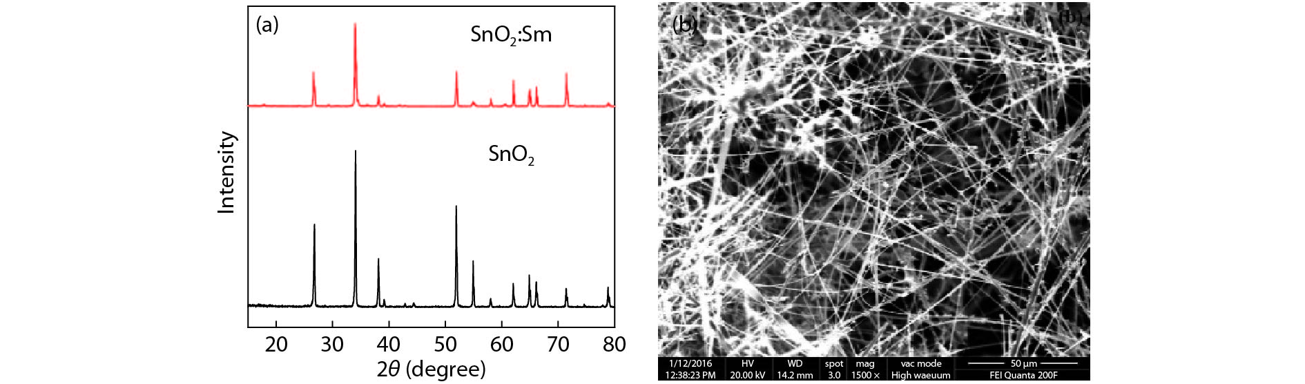
Fig. 1.
(Color online) Structure and morphology characterization of as-synthesized product. (a) XRD pattern. (b) FESEM image.
ARTICLES
Huiying Zhou1, , Haiping Shi2 and Baochang Cheng2, 3,
Corresponding author: Huiying Zhou, 307315121@qq.com (H. Y. Zhou); Baochang Cheng, bcheng@vip.sina.com (B. C. Cheng)
Abstract: For nanostructure SnO2, it is very difficult for its electric properties to accurately control due to the presence of abundant surface states. The introduction of Sm can improve the traps in surface space charge region of SnO2 nanowires, resulting in a controllable storage charge effect. For the single nanowire-based two-terminal device, two surface state-related back-to-back diodes are formed. At a relatively large voltage, electrons can be injected into the traps in surface space charge region from negative electrode, resulting in a decrease of surface barrier connected with negative electrode, and contrarily electrons can be extracted from the traps in surface space charge region into positive electrode, resulting in an increase of surface barrier connected with positive electrode. The reversible injection and extraction induce a nonvolatile resistive switching memory effect.
Key words: nanowire, surface state, trap, memory effect
| [1] |
Cheng B, Ouyang Z, Chen C, et al. Individual Zn2SnO4-sheathed ZnO heterostructure nanowires for efficient resistive switching memory controlled by interface states. Sci Rep, 2013, 3, 3249 doi: 10.1038/srep03249
|
| [2] |
Shi H, Cheng B, Cai Q, et al. Surface state controlled ultrahigh selectivity and sensitivity for UV photodetectors based on individual SnO2 nanowires. J Mater Chem C, 2016, 4(36), 8399 doi: 10.1039/C6TC02420C
|
| [3] |
Barth S, Hernandez-Ramirez F, Holmes J, et al. Synthesis and applications of one-dimensional semiconductors. Prog Mater Sci, 2010, 55(6), 563 doi: 10.1016/j.pmatsci.2010.02.001
|
| [4] |
Liang F, Zhang J, Wang Z, et al. Broadband, ultrafast, self-driven photodetector based on Cs-doped FAPbI3 perovskite thin film. Adv Opt Mater, 2017, 5(22), 1700081 doi: 10.1002/adom.201700654
|
| [5] |
Devan R, Patil A, Lin J, et al. One-dimensional metal-oxide nanostructures: recent developments in synthesis, characterization, and applications. Adv Funct Mater, 2012, 22(16), 3326 doi: 10.1002/adfm.201201008
|
| [6] |
Utama M, Zhang J, Chen R, et al. Synthesis and optical properties of II–VI 1D nanostructures. Nanoscale, 2012, 4(5), 1422 doi: 10.1039/c1nr11612f
|
| [7] |
Wang F, Dong A, Buhro W. Solution-liquid-solid synthesis, properties, and applications of one-dimensional colloidal semiconductor nanorods and nanowires. Chem Rev, 2016, 116(18), 10888 doi: 10.1021/acs.chemrev.5b00701
|
| [8] |
Xia Y, Yang P, Sun Y, et al. One-dimensional nanostructures: synthesis, characterization, and applications. Adv Mater, 2003, 15(5), 353 doi: 10.1002/adma.200390087
|
| [9] |
Ouyang W, Teng F, Fang X. High performance BiOCl nanosheets/TiO2 nanotube arrays heterojunction UV photodetector: the influences of self-induced inner electric fields in the BiOCl nanosheets. Adv Funct Mater, 2018, 28(16), 1707178 doi: 10.1002/adfm.201707178
|
| [10] |
Yu P, Hu K, Chen H, et al. Novel p-p heterojunctions self-powered broadband photodetectors with ultrafast speed and high responsivity. Adv Funct Mater, 2017, 27(38), 1703166 doi: 10.1002/adfm.201703166
|
| [11] |
Chen H, Yang S. Hierarchical nanostructures of metal oxides for enhancing charge separation and transport in photoelectrochemical solar energy conversion systems. Nanoscale Horiz, 2016, 1(2), 96 doi: 10.1039/C5NH00033E
|
| [12] |
LaPierre R, Robson M, Azizur-Rahman K, et al. A review of III–V nanowire infrared photodetectors and sensors. J Appl Phys, 2017, 50(12), 123001 doi: 10.1088/1361-6463/aa5ab3
|
| [13] |
Liu M, Peng Y, Wu Z. Post-growth assembly of nanowires for integration of nanodevices. Adv Mater Res, 2012, 476–478, 1463 doi: 10.4028/www.scientific.net/AMR.476-478.1463
|
| [14] |
Zhao H, Zhang Q, Weng Y. Deep surface trap filling by photoinduced carriers and interparticle electron transport observed in TiO2 nanocrystalline film with time-resolved visible and mid-IR transient spectroscopies. J Phys Chem C, 2007, 111(9), 3762 doi: 10.1021/jp0645566
|
| [15] |
Cheng B, Xu J, Ouyang Z, et al. Individual Ohmic contacted ZnO/Zn2SnO4 radial heterostructured nanowires as photodetectors with a broad-spectral-response: injection of electrons into/from interface states. J Mater Chem C, 2014, 2(10), 1808 doi: 10.1039/c3tc32059f
|
| [16] |
Kar S, Chaudhuri S. Shape selective growth of CdS one-dimensional nanostructures by a thermal evaporation process. J Phys Chem B, 2006, 110(10), 4542 doi: 10.1021/jp056058n
|
| [17] |
Tian W, Wang Y D, Chen L, et al. Self-powered nanoscale photodetectors. Small, 2017, 13(45), 1701848 doi: 10.1002/smll.201701848
|
| [18] |
Zhang T, Li Z, Wang J, et al. Broadband photodetector based on carbon nanotube thin film/single layer graphene Schottky junction. Sci Rep, 2016, 6, 38569 doi: 10.1038/srep38569
|
| [19] |
Cheng B, Zhao J, Xiao L, et al. PMMA interlayer-modulated memory effects by space charge polarization in resistive switching based on CuSCN nanopyramids/ZnO-nanorods p–n heterojunction. Sci Rep, 2015, 5, 17859 doi: 10.1038/srep17859
|
| [20] |
Zhao J, Cheng B, Xiao Y, et al. Ultrahigh performance negative thermal-resistance switching based on individual ZnO:K, Cl micro/nanowires for multibit nonvolatile resistance random access memory dual-written/erased repeatedly by temperature or bias. J Mater Chem C, 2015, 3(47), 12220 doi: 10.1039/C5TC02824H
|
| [21] |
Zhao J, Cheng B, Xiao Y, et al. Gate-free controlled multibit memories based on individual ZnO:In micro/nanowire back-to-back diodes. Adv Electron Mater, 2016, 2(4), 1500395 doi: 10.1002/aelm.201500395
|
| [22] |
Cheng B, Wu G, Ouyang Z, et al. Effects of interface states on photoexcited carriers in ZnO/Zn2SnO4 type-II radial heterostructure nanowires. ACS Appl Mater Interfaces, 2014, 6(6), 4057 doi: 10.1021/am405569k
|
| [23] |
Tao L, Cinquanta E, Chiappe D, et al. Cinicene field-effect transistors operating at room temperature. Nat Nanotechnol, 2015, 10(3), 227 doi: 10.1038/nnano.2014.325
|
| [24] |
Cheng B, Xu J, Ouyang Z, et al. Individual ZnO nanowires for photodetectors with wide response range from solar-blind ultraviolet to near-infrared modulated by bias voltage and illumination intensity. Opt Express, 2013, 21(24), 29719 doi: 10.1364/OE.21.029719
|
| [25] |
Cadafalch Gazquez G, Lei S, George A, et al. Low-Cost, large-area, facile, and rapid fabrication of aligned ZnO nanowire device arrays. ACS Appl Mater Interfaces, 2016, 8, 13466 doi: 10.1021/acsami.6b01594
|
| [26] |
Tong T, Wang S, Zhao J, et al. Erasable memory properties of spectral selectivity modulated by temperature and bias in an individual CdS nanobelt-based photodetector. Nanoscale Horiz, 2019, 4(1), 138 doi: 10.1039/C8NH00182K
|
| [27] |
Wang S, Zhao J, Tong T, et al. Bias-controlled tunable electronic transport with memory characteristics in an individual ZnO nanowire for realization of a self-driven UV photodetector with two symmetrical electrodes. ACS Appl Mater Interfaces, 2019, 11(16), 14932 doi: 10.1021/acsami.9b00267
|
| [28] |
Zheng J, Cheng B, Wu Fu, et al. Modulation of surface trap induced resistive switching by electrode annealing in individual PbS micro/nanowire-based devices for resistance random access memory. ACS Appl Mater Interfaces, 2014, 6(23), 20812 doi: 10.1021/am505101w
|
| [29] |
Cheng B, Yu X, Liu H, et al. Enhanced effect of electron-hole plasma emission in Dy, Li codoped ZnO nanostructures. J Appl Phys, 2009, 105(1), 014311 doi: 10.1063/1.3060423
|
| [30] |
Cheng, B, Zhang Z, Liu H, e al. Power- and energy-dependent photoluminescence of Eu3+ incorporated and segregated ZnO polycrystalline nanobelts synthesized by a facile combustion method followed by heat treatment. J Mater Chem, 2010, 20(36), 7821 doi: 10.1039/c0jm00804d
|
| [31] |
Cheng B, Jiao J, Sun W, et al. Lattice variation and Raman spectroscopy in hierarchical heterostructures of zinc antimonate nanoislands on ZnO nanobelts. Nanotechnology, 2010, 21(2), 025704 doi: 10.1088/0957-4484/21/2/025704
|
| [32] |
Gomer R. Field emission and field ionization. American Institute of Physics, New York, 1992
|
| [33] |
Sze S, Ng K. Physics of semiconductor devices. 3rd ed. NJ: John Wiley & Sons, 2007
|


Article views: 4237 Times PDF downloads: 50 Times Cited by: 0 Times
Received: 08 October 2019 Revised: 28 October 2019 Online: Accepted Manuscript: 18 November 2019Uncorrected proof: 19 November 2019Published: 02 January 2020
| Citation: |
Huiying Zhou, Haiping Shi, Baochang Cheng. Surface traps-related nonvolatile resistive switching memory effect in a single SnO2:Sm nanowire[J]. Journal of Semiconductors, 2020, 41(1): 012101. doi: 10.1088/1674-4926/41/1/012101
****
H Y Zhou, H P Shi, B C Cheng, Surface traps-related nonvolatile resistive switching memory effect in a single SnO2:Sm nanowire[J]. J. Semicond., 2020, 41(1): 012101. doi: 10.1088/1674-4926/41/1/012101.

|
| [1] |
Cheng B, Ouyang Z, Chen C, et al. Individual Zn2SnO4-sheathed ZnO heterostructure nanowires for efficient resistive switching memory controlled by interface states. Sci Rep, 2013, 3, 3249 doi: 10.1038/srep03249
|
| [2] |
Shi H, Cheng B, Cai Q, et al. Surface state controlled ultrahigh selectivity and sensitivity for UV photodetectors based on individual SnO2 nanowires. J Mater Chem C, 2016, 4(36), 8399 doi: 10.1039/C6TC02420C
|
| [3] |
Barth S, Hernandez-Ramirez F, Holmes J, et al. Synthesis and applications of one-dimensional semiconductors. Prog Mater Sci, 2010, 55(6), 563 doi: 10.1016/j.pmatsci.2010.02.001
|
| [4] |
Liang F, Zhang J, Wang Z, et al. Broadband, ultrafast, self-driven photodetector based on Cs-doped FAPbI3 perovskite thin film. Adv Opt Mater, 2017, 5(22), 1700081 doi: 10.1002/adom.201700654
|
| [5] |
Devan R, Patil A, Lin J, et al. One-dimensional metal-oxide nanostructures: recent developments in synthesis, characterization, and applications. Adv Funct Mater, 2012, 22(16), 3326 doi: 10.1002/adfm.201201008
|
| [6] |
Utama M, Zhang J, Chen R, et al. Synthesis and optical properties of II–VI 1D nanostructures. Nanoscale, 2012, 4(5), 1422 doi: 10.1039/c1nr11612f
|
| [7] |
Wang F, Dong A, Buhro W. Solution-liquid-solid synthesis, properties, and applications of one-dimensional colloidal semiconductor nanorods and nanowires. Chem Rev, 2016, 116(18), 10888 doi: 10.1021/acs.chemrev.5b00701
|
| [8] |
Xia Y, Yang P, Sun Y, et al. One-dimensional nanostructures: synthesis, characterization, and applications. Adv Mater, 2003, 15(5), 353 doi: 10.1002/adma.200390087
|
| [9] |
Ouyang W, Teng F, Fang X. High performance BiOCl nanosheets/TiO2 nanotube arrays heterojunction UV photodetector: the influences of self-induced inner electric fields in the BiOCl nanosheets. Adv Funct Mater, 2018, 28(16), 1707178 doi: 10.1002/adfm.201707178
|
| [10] |
Yu P, Hu K, Chen H, et al. Novel p-p heterojunctions self-powered broadband photodetectors with ultrafast speed and high responsivity. Adv Funct Mater, 2017, 27(38), 1703166 doi: 10.1002/adfm.201703166
|
| [11] |
Chen H, Yang S. Hierarchical nanostructures of metal oxides for enhancing charge separation and transport in photoelectrochemical solar energy conversion systems. Nanoscale Horiz, 2016, 1(2), 96 doi: 10.1039/C5NH00033E
|
| [12] |
LaPierre R, Robson M, Azizur-Rahman K, et al. A review of III–V nanowire infrared photodetectors and sensors. J Appl Phys, 2017, 50(12), 123001 doi: 10.1088/1361-6463/aa5ab3
|
| [13] |
Liu M, Peng Y, Wu Z. Post-growth assembly of nanowires for integration of nanodevices. Adv Mater Res, 2012, 476–478, 1463 doi: 10.4028/www.scientific.net/AMR.476-478.1463
|
| [14] |
Zhao H, Zhang Q, Weng Y. Deep surface trap filling by photoinduced carriers and interparticle electron transport observed in TiO2 nanocrystalline film with time-resolved visible and mid-IR transient spectroscopies. J Phys Chem C, 2007, 111(9), 3762 doi: 10.1021/jp0645566
|
| [15] |
Cheng B, Xu J, Ouyang Z, et al. Individual Ohmic contacted ZnO/Zn2SnO4 radial heterostructured nanowires as photodetectors with a broad-spectral-response: injection of electrons into/from interface states. J Mater Chem C, 2014, 2(10), 1808 doi: 10.1039/c3tc32059f
|
| [16] |
Kar S, Chaudhuri S. Shape selective growth of CdS one-dimensional nanostructures by a thermal evaporation process. J Phys Chem B, 2006, 110(10), 4542 doi: 10.1021/jp056058n
|
| [17] |
Tian W, Wang Y D, Chen L, et al. Self-powered nanoscale photodetectors. Small, 2017, 13(45), 1701848 doi: 10.1002/smll.201701848
|
| [18] |
Zhang T, Li Z, Wang J, et al. Broadband photodetector based on carbon nanotube thin film/single layer graphene Schottky junction. Sci Rep, 2016, 6, 38569 doi: 10.1038/srep38569
|
| [19] |
Cheng B, Zhao J, Xiao L, et al. PMMA interlayer-modulated memory effects by space charge polarization in resistive switching based on CuSCN nanopyramids/ZnO-nanorods p–n heterojunction. Sci Rep, 2015, 5, 17859 doi: 10.1038/srep17859
|
| [20] |
Zhao J, Cheng B, Xiao Y, et al. Ultrahigh performance negative thermal-resistance switching based on individual ZnO:K, Cl micro/nanowires for multibit nonvolatile resistance random access memory dual-written/erased repeatedly by temperature or bias. J Mater Chem C, 2015, 3(47), 12220 doi: 10.1039/C5TC02824H
|
| [21] |
Zhao J, Cheng B, Xiao Y, et al. Gate-free controlled multibit memories based on individual ZnO:In micro/nanowire back-to-back diodes. Adv Electron Mater, 2016, 2(4), 1500395 doi: 10.1002/aelm.201500395
|
| [22] |
Cheng B, Wu G, Ouyang Z, et al. Effects of interface states on photoexcited carriers in ZnO/Zn2SnO4 type-II radial heterostructure nanowires. ACS Appl Mater Interfaces, 2014, 6(6), 4057 doi: 10.1021/am405569k
|
| [23] |
Tao L, Cinquanta E, Chiappe D, et al. Cinicene field-effect transistors operating at room temperature. Nat Nanotechnol, 2015, 10(3), 227 doi: 10.1038/nnano.2014.325
|
| [24] |
Cheng B, Xu J, Ouyang Z, et al. Individual ZnO nanowires for photodetectors with wide response range from solar-blind ultraviolet to near-infrared modulated by bias voltage and illumination intensity. Opt Express, 2013, 21(24), 29719 doi: 10.1364/OE.21.029719
|
| [25] |
Cadafalch Gazquez G, Lei S, George A, et al. Low-Cost, large-area, facile, and rapid fabrication of aligned ZnO nanowire device arrays. ACS Appl Mater Interfaces, 2016, 8, 13466 doi: 10.1021/acsami.6b01594
|
| [26] |
Tong T, Wang S, Zhao J, et al. Erasable memory properties of spectral selectivity modulated by temperature and bias in an individual CdS nanobelt-based photodetector. Nanoscale Horiz, 2019, 4(1), 138 doi: 10.1039/C8NH00182K
|
| [27] |
Wang S, Zhao J, Tong T, et al. Bias-controlled tunable electronic transport with memory characteristics in an individual ZnO nanowire for realization of a self-driven UV photodetector with two symmetrical electrodes. ACS Appl Mater Interfaces, 2019, 11(16), 14932 doi: 10.1021/acsami.9b00267
|
| [28] |
Zheng J, Cheng B, Wu Fu, et al. Modulation of surface trap induced resistive switching by electrode annealing in individual PbS micro/nanowire-based devices for resistance random access memory. ACS Appl Mater Interfaces, 2014, 6(23), 20812 doi: 10.1021/am505101w
|
| [29] |
Cheng B, Yu X, Liu H, et al. Enhanced effect of electron-hole plasma emission in Dy, Li codoped ZnO nanostructures. J Appl Phys, 2009, 105(1), 014311 doi: 10.1063/1.3060423
|
| [30] |
Cheng, B, Zhang Z, Liu H, e al. Power- and energy-dependent photoluminescence of Eu3+ incorporated and segregated ZnO polycrystalline nanobelts synthesized by a facile combustion method followed by heat treatment. J Mater Chem, 2010, 20(36), 7821 doi: 10.1039/c0jm00804d
|
| [31] |
Cheng B, Jiao J, Sun W, et al. Lattice variation and Raman spectroscopy in hierarchical heterostructures of zinc antimonate nanoislands on ZnO nanobelts. Nanotechnology, 2010, 21(2), 025704 doi: 10.1088/0957-4484/21/2/025704
|
| [32] |
Gomer R. Field emission and field ionization. American Institute of Physics, New York, 1992
|
| [33] |
Sze S, Ng K. Physics of semiconductor devices. 3rd ed. NJ: John Wiley & Sons, 2007
|

 WeChat ID
Journal of Semiconductors © 2017 All Rights Reserved 京ICP备05085259号-2

 DownLoad: