| [1] |
Ielmini D. Brain-inspired computing with resistive switching memory (RRAM): Devices, synapses and neural networks. Microelectron Eng, 2018, 190, 44 doi: 10.1016/j.mee.2018.01.009 |
| [2] |
Bliss T V P, Collingridge G L. A synaptic model of memory: long-term potentiation in the hippocampus. Nature, 1993, 361(6407), 31 doi: 10.1038/361031a0 |
| [3] |
|
| [4] |
Yao P, Wu H, Gao B, et al. Fully hardware-implemented memristor convolutional neural network. Nature, 2020, 577(7792), 641 doi: 10.1038/s41586-020-1942-4 |
| [5] |
Cai F, Correll J M, Lee S H, et al. A fully integrated reprogrammable memristor–CMOS system for efficient multiply-accumulate operations. Nat Electron, 2019, 2(7), 290 doi: 10.1038/s41928-019-0270-x |
| [6] |
Qian W H, Cheng X F, Zhou J, et al. Lead-free perovskite MASnBr 3-based memristor for quaternary information storage. InfoMat, 2019 doi: 10.1002/inf2.12066 |
| [7] |
Pang Y, Gao B, Lin B, et al. Memristors for hardware security applications. Adv Electron Mater, 2019, 5(9), 1800872 doi: 10.1002/aelm.201800872 |
| [8] |
Chen X, Zhou Y, Roy V A L, et al. Evolutionary metal oxide clusters for novel applications: toward high-density data storage in nonvolatile memories. Adv Mater, 2018, 30(3), 1703950 doi: 10.1002/adma.201703950 |
| [9] |
Tan Z H, Yang R, Terabe K, et al. Synaptic metaplasticity realized in oxide memristive devices. Adv Mater, 2016, 28(2), 377 doi: 10.1002/adma.201503575 |
| [10] |
Han S T, Zhou Y, Roy V A L. Towards the development of flexible non-volatile memories. Adv Mater, 2013, 25(38), 5425 doi: 10.1002/adma.201301361 |
| [11] |
Yoo S, Eom T, Gwon T, et al. Bipolar resistive switching behavior of an amorphous Ge 2Sb 2Te 5 thin films with a Te layer. Nanoscale, 2015, 7(14), 6340 doi: 10.1039/C5NR01361E |
| [12] |
Gu C, Lee J S. Flexible hybrid organic-inorganic perovskite memory. ACS nano, 2016, 10(5), 5413 doi: 10.1021/acsnano.6b01643 |
| [13] |
Tian H, Zhao L, Wang X, et al. Extremely low operating current resistive memory based on exfoliated 2D perovskite single crystals for neuromorphic computing. ACS Nano, 2017, 11(12), 12247 doi: 10.1021/acsnano.7b05726 |
| [14] |
Zhou F, Liu Y, Shen X, et al. Low-voltage, optoelectronic CH 3NH 3PbI 3– xCl x memory with integrated sensing and logic operations. Adv Funct Mater, 2018, 28(15), 1800080 doi: 10.1002/adfm.201800080 |
| [15] |
Stranks S D, Snaith H J. Metal-halide perovskites for photovoltaic and light-emitting devices. Nat Nanotechnol, 2015, 10(5), 391 doi: 10.1038/nnano.2015.90 |
| [16] |
Chen Q, De Marco N, Yang Y M, et al. Under the spotlight: The organic-inorganic hybrid halide perovskite for optoelectronic applications. Nano Today, 2015, 10(3), 355 doi: 10.1016/j.nantod.2015.04.009 |
| [17] |
Dong Q, Fang Y, Shao Y, et al. Electron-hole diffusion lengths > 175 μm in solution-grown CH 3NH 3PbI 3 single crystals. Science, 2015, 347(6225), 967 doi: 10.1126/science.aaa5760 |
| [18] |
Lee M M, Teuscher J, Miyasaka T, et al. Efficient hybrid solar cells based on meso-superstructure organometal halide perovskites. Science, 2012, 338(6107), 643 doi: 10.1126/science.1228604 |
| [19] |
Fang Y, Dong Q, Shao Y, et al. Highly narrowband perovskite single-crystal photodetectors enabled by surface-charge recombination. Nat Photonics, 2015, 9(10), 679 doi: 10.1038/nphoton.2015.156 |
| [20] |
Shi D, Adinolfi V, Comin R, et al. Low trap-state density and long carrier diffusion in organolead trihalide perovskite single crystals. Science, 2015, 347(6221), 519 doi: 10.1126/science.aaa2725 |
| [21] |
Li F, Wang H, Kufer D, et al. Ultrahigh carrier mobility achieved in photoresponsive hybrid perovskite films via coupling with single-walled carbon nanotubes. Adv Mater, 2017, 29(16), 1602432 doi: 10.1002/adma.201602432 |
| [22] |
Anand B, Sampat S, Danilov E O, et al. Broadband transient absorption study of photoexcitations in lead halide perovskites: Towards a multiband picture. Phys Rev B, 2016, 93(16), 161205 doi: 10.1103/PhysRevB.93.161205 |
| [23] |
Tan Z K, Moghaddam R S, Lai M L, et al. Bright light-emitting diodes based on organometal halide perovskite. Nat Nanotechnol, 2014, 9(9), 687 doi: 10.1038/nnano.2014.149 |
| [24] |
Senanayak S P, Yang B, Thomas T H, et al. Understanding charge transport in lead iodide perovskite thin-film field-effect transistors. Sci Adv, 2017, 3(1), e1601935 doi: 10.1126/sciadv.1601935 |
| [25] |
Wang K, Wu C, Yang D, et al. Quasi-two-dimensional halide perovskite single crystal photodetector. ACS Nano, 2018, 12(5), 4919 doi: 10.1021/acsnano.8b01999 |
| [26] |
Yang T Y, Gregori G, Pellet N, et al. The significance of ion conduction in a hybrid organic-inorganic lead-iodide-based perovskite photosensitizer. Angew Chem Int Ed, 2015, 54(27), 7905 doi: 10.1002/anie.201500014 |
| [27] |
Haruyama J, Sodeyama K, Han L, et al. First-principles study of ion diffusion in perovskite solar cell sensitizers. J Am Chem Soc, 2015, 137(32), 10048 doi: 10.1021/jacs.5b03615 |
| [28] |
Chua L. Memristor-the missing circuit element. IEEE Trans Circuit Theory, 1971, 18(5), 507 doi: 10.1109/TCT.1971.1083337 |
| [29] |
Strukov D B, Snider G S, Stewart D R, et al. The missing memristor found. Nature, 2008, 453(7191), 80 doi: 10.1038/nature06932 |
| [30] |
Yoon J H, Zhang J, Ren X, et al. Truly electroforming-free and low-energy memristors with preconditioned conductive tunneling paths. Adv Funct Mater, 2017, 27(35), 1702010 doi: 10.1002/adfm.201702010 |
| [31] |
Ielmini D, Wong H S P. In-memory computing with resistive switching devices. Nat Electron, 2018, 1(6), 333 doi: 10.1038/s41928-018-0092-2 |
| [32] |
Xiao Z, Yuan Y, Shao Y, et al. Giant switchable photovoltaic effect in organometal trihalide perovskite devices. Nat Mater, 2015, 14(2), 193 doi: 10.1038/nmat4150 |
| [33] |
Xu J, Zhao X, Wang Z, et al. Biodegradable natural pectin-based flexible multilevel resistive switching memory for transient electronics. Small, 2019, 15(4), 1803970 doi: 10.1002/smll.201803970 |
| [34] |
Yan X, Wang K, Zhao J, et al. A new memristor with 2D Ti 3C 2T x MXene flakes as an artificial bio-synapse. Small, 2019, 15(25), 1900107 doi: 10.1002/smll.201900107 |
| [35] |
Yu F, Zhu L, Xiao H, et al. Restickable oxide neuromorphic transistors with spike-timing-dependent plasticity and pavlovian associative learning activities. Adv Funct Mater, 2018, 28(44), 1804025 doi: 10.1002/adfm.201804025 |
| [36] |
Yan X, Li X, Zhou Z, et al. Flexible transparent organic artificial synapse based on the tungsten/egg albumen/indium tin oxide/polyethylene terephthalate memristor. ACS Appl Mater Interfaces, 2019, 11(20), 18654 doi: 10.1021/acsami.9b04443 |
| [37] |
Yan X, Zhao Q, Chen A P, et al. Vacancy-induced synaptic behavior in 2D WS 2 nanosheet-based memristor for low-power neuromorphic computing. Small, 2019, 15(24), 1901423 doi: 10.1002/smll.201901423 |
| [38] |
Choi S, Tan S H, Li Z, et al. SiGe epitaxial memory for neuromorphic computing with reproducible high performance based on engineered dislocations. Nat Mater, 2018, 17(4), 335 doi: 10.1038/s41563-017-0001-5 |
| [39] |
Yan X, Zhao J, Liu S, et al. Memristor with Ag-cluster-doped TiO 2 films as artificial synapse for Neuroinspired computing. Adv Funct Mater, 2018, 28(1), 1705320 doi: 10.1002/adfm.201705320 |
| [40] |
Zhu X, Li D, Liang X, et al. Ionic modulation and ionic coupling effects in MoS 2 devices for neuromorphic computing. Nat Mater, 2019, 18(2), 141 doi: 10.1038/s41563-018-0248-5 |
| [41] |
Muenstermann R, Menke T, Dittmann R, et al. Coexistence of filamentary and homogeneous resistive switching in Fe-doped SrTiO 3 thin-film memristive devices. Adv Mater, 2010, 22(43), 4819 doi: 10.1002/adma.201001872 |
| [42] |
Jeong H Y, Lee J Y, Choi S Y. Interface-engineered amorphous TiO 2-based resistive memory devices. Adv Funct Mater, 2010, 20(22), 3912 doi: 10.1002/adfm.201001254 |
| [43] |
Yang Y, Huang R. Probing memristive switching in nanoionic devices. Nat Electron, 2018, 1(5), 274 doi: 10.1038/s41928-018-0069-1 |
| [44] |
Budiman F, Hernowo D G O, Pandey R R, et al. Recent progress on fabrication of memristor and transistor-based neuromorphic devices for high signal processing speed with low power consumption. Jpn J Appl Phys, 2018, 57(3S2), 03EA06 doi: 10.7567/JJAP.57.03EA06 |
| [45] |
Chen J Y, Huang C W, Chiu C H, et al. Switching kinetic of VCM-based memristor: evolution and positioning of nanofilament. Adv Mater, 2015, 27(34), 5028 doi: 10.1002/adma.201502758 |
| [46] |
Liu Q, Sun J, Lv H, et al. Real-time observation on dynamic growth/dissolution of conductive filaments in oxide-electrolyte based ReRAM. Adv Mater, 2012, 24(14), 1844 doi: 10.1002/adma.201104104 |
| [47] |
Yang Y, Gao P, Li L, et al. Electrochemical dynamics of nanoscale metallic inclusions in dielectrics. Nat Commun, 2014, 5(1), 1 doi: 10.1038/ncomms5232 |
| [48] |
Yang Y, Lee J, Lee S, et al. Oxide resistive memory with functionalized graphene as built-in selector element. Adv Mater, 2014, 26(22), 3693 doi: 10.1002/adma.201400270 |
| [49] |
Kim S, Choi S H, Lu W. Comprehensive physical model of dynamic resistive switching in an oxide memristor. ACS Nano, 2014, 8(3), 2369 doi: 10.1021/nn405827t |
| [50] |
Xue W, Liu G, Zhong Z, et al. A 1D vanadium dioxide nanochannel constructed via electric-field-induced ion transport and its superior metal-insulator transition. Adv Mater, 2017, 29(39), 1702162 doi: 10.1002/adma.201702162 |
| [51] |
Wang Z Q, Xu H Y, Li X H, et al. Memristors: synaptic learning and memory functions achieved using oxygen ion migration/diffusion in an amorphous InGaZnO Memristor. Adv Funct Mater, 2012, 22(13), 2758 doi: 10.1002/adfm.201290076 |
| [52] |
Chang C F, Chen J Y, Huang C W, et al. Direct observation of dual-filament switching behaviors in Ta 2O 5-based memristors. Small, 2017, 13(15), 1603116 doi: 10.1002/smll.201603116 |
| [53] |
Yan X, Zhou Z, Ding B, et al. Superior resistive switching memory and biological synapse properties based on a simple TiN/SiO 2/p-Si tunneling junction structure. J Mater Chem C, 2017, 5(9), 2259 doi: 10.1039/C6TC04261A |
| [54] |
Gao S, Liu G, Yang H, et al. An oxide Schottky junction artificial optoelectronic synapse. ACS Nano, 2019, 13(2), 2634 doi: 10.1021/acsnano.9b00340 |
| [55] |
Tan H, Liu G, Zhu X, et al. An optoelectronic resistive switching memory with integrated demodulating and arithmetic functions. Adv Mater, 2015, 27(17), 2797 doi: 10.1002/adma.201500039 |
| [56] |
Murphy E L, Good R H Jr. Thermionic emission, field emission, and the transition region. Phys Rev, 1956, 102(6), 1464 doi: 10.1103/PhysRev.102.1464 |
| [57] |
Emtage P R, Tantraporn W. Schottky emission through thin insulating films. Phys Rev Lett, 1962, 8(7), 267 doi: 10.1103/PhysRevLett.8.267 |
| [58] |
Simmons J G. Electric tunnel effect between dissimilar electrodes separated by a thin insulating film. J Appl Phys, 1963, 34(9), 2581 doi: 10.1063/1.1729774 |
| [59] |
Svensson C, Lundström I. Trap-assisted charge injection in MNOS structures. J Appl Phys, 1973, 44(10), 4657 doi: 10.1063/1.1662016 |
| [60] |
Ma Y, Wang S, Zheng L, et al. Recent research developments of perovskite solar cells. Chin J Chem, 2014, 32(10), 957 doi: 10.1002/cjoc.201400435 |
| [61] |
Shi Z, Guo J, Chen Y, et al. Lead-free organic-inorganic hybrid Perovskites for photovoltaic applications: recent advances and perspectives. Adv Mater, 2017, 29(16), 1605005 doi: 10.1002/adma.201605005 |
| [62] |
Miyata A, Mitioglu A, Plochocka P, et al. Direct measurement of the exciton binding energy and effective masses for charge carriers in organic-inorganic tri-halide perovskites. Nat Phys, 2015, 11(7), 582 doi: 10.1038/nphys3357 |
| [63] |
Stoumpos C C, Kanatzidis M G. Halide perovskites: poor man's high-performance semiconductors. Adv Mater, 2016, 28(28), 5778 doi: 10.1002/adma.201600265 |
| [64] |
Yao J S, Ge J, Han B N, et al. Ce 3+-doping to modulate photoluminescence kinetics for efficient CsPbBr 3 nanocrystals-based light-emitting diodes. J Am Chem Soc, 2018, 140(10), 3626 doi: 10.1021/jacs.7b11955 |
| [65] |
Swarnkar A, Ravi V K, Nag A. Beyond colloidal cesium lead halide perovskite nanocrystals: analogous metal halides and doping. ACS Energy Lett, 2017, 2(5), 1089 doi: 10.1021/acsenergylett.7b00191 |
| [66] |
Liang J, Liu J, Jin Z. All-inorganic halide perovskites for optoelectronics: progress and prospects. Sol RRL, 2017, 1(10), 1700086 doi: 10.1002/solr.201700086 |
| [67] |
Yoo E J, Lyu M, Yun J H, et al. Resistive switching behavior in organic-inorganic hybrid CH 3NH 3PbI 3– xCl x perovskite for resistive random-access memory devices. Adv Mater, 2015, 27(40), 6170 doi: 10.1002/adma.201502889 |
| [68] |
Wang H, Kim D H. Perovskite-based photodetectors: materials and devices. Chem Soc Rev, 2017, 46(17), 5204 doi: 10.1039/C6CS00896H |
| [69] |
Zhou J, Huang J. Photodetectors based on organic-inorganic hybrid lead halide perovskites. Adv Sci, 2018, 5(1), 1700256 doi: 10.1002/advs.201700256 |
| [70] |
Choi J, Han J S, Hong K, et al. Organic–inorganic hybrid halide perovskites for memories, transistors, and artificial synapses. Adv Mater, 2018, 30(42), 1704002 doi: 10.1002/adma.201704002 |
| [71] |
Tress W. Metal halide perovskites as mixed electronic-ionic conductors: challenges and opportunities from hysteresis to memristivity. J Phys Chem Lett, 2017, 8(13), 3106 doi: 10.1021/acs.jpclett.7b00975 |
| [72] |
Ma Z, Li F, Qi G, et al. Structural stability and optical properties of two-dimensional perovskite-like CsPb 2Br 5 microplates in response to pressure. Nanoscale, 2019, 11(3), 820 doi: 10.1039/C8NR05684F |
| [73] |
Xing G, Mathews N, Sun S, et al. Long-range balanced electron- and hole-transport lengths in organic–inorganic CH 3NH 3PbI 3. Science, 2013, 342(6156), 344 doi: 10.1126/science.1243167 |
| [74] |
Weidman M C, Seitz M, Stranks S D, et al. Highly tunable colloidal perovskite nanoplatelets through variable cation, metal, and halide composition. ACS Nano, 2016, 10(8), 7830 doi: 10.1021/acsnano.6b03496 |
| [75] |
Cuhadar C, Kim S G, Yang J M, et al. All-inorganic bismuth halide perovskite-like materials A 3Bi 2I 9 and A 3Bi 1.8Na 0.2I 8.6 (A = Rb and Cs) for low-voltage switching resistive memory. ACS Appl Mater Interfaces, 2018, 10(35), 29741 doi: 10.1021/acsami.8b07103 |
| [76] |
Acharyya P, Pal P, Samanta P K, et al. Single pot synthesis of indirect band gap 2D CsPb 2Br 5 nanosheets from direct band gap 3D CsPbBr 3 nanocrystals and the origin of their luminescence properties. Nanoscale, 2019, 11(9), 4001 doi: 10.1039/C8NR09349K |
| [77] |
Iwahara H. Ionic conduction in perovskite-type compounds. In: Perovskite Oxide for Solid Oxide Fuel Cells. Boston: Springer, 2009, 45
|
| [78] |
Li C, Tscheuschner S, Paulus F, et al. Iodine migration and its effect on hysteresis in perovskite solar cells. Adv Mater, 2016, 28(12), 2446 doi: 10.1002/adma.201503832 |
| [79] |
Leng K, Abdelwahab I, Verzhbitskiy I, et al. Molecularly thin two-dimensional hybrid perovskites with tunable optoelectronic properties due to reversible surface relaxation. Nat Mater, 2018, 17(10), 908 doi: 10.1038/s41563-018-0164-8 |
| [80] |
Qian L, Sun Y, Wu M, et al. A lead-free two-dimensional perovskite for a high-performance flexible photoconductor and a light-stimulated synaptic device. Nanoscale, 2018, 10(15), 6837 doi: 10.1039/C8NR00914G |
| [81] |
Prezioso M, Merrikh-Bayat F, Hoskins B D, et al. Training and operation of an integrated neuromorphic network based on metal–oxide memristors. Nature, 2015, 521(7550), 61 doi: 10.1038/nature14441 |
| [82] |
Liu S J, Lin Z H, Zhao Q, et al. Flash-memory effect for polyfluorenes with on-chain iridium (III) complexes. Adv Funct Mater, 2011, 21(5), 979 doi: 10.1002/adfm.201001884 |
| [83] |
Zhao L, Wang K, Wei W, et al. High-performance flexible sensing devices based on polyaniline/MXene nanocomposites. InfoMat, 2019, 1(3), 407 doi: 10.1002/inf2.12032 |
| [84] |
Lin G, Lin Y, Cui R, et al. An organic-inorganic hybrid perovskite logic gate for better computing. J Mater Chem C, 2015, 3(41), 10793 doi: 10.1039/C5TC02270C |
| [85] |
Yan K, Peng M, Yu X, et al. High-performance perovskite memristor based on methyl ammonium lead halides. J Mater Chem C, 2016, 4(7), 1375 doi: 10.1039/C6TC00141F |
| [86] |
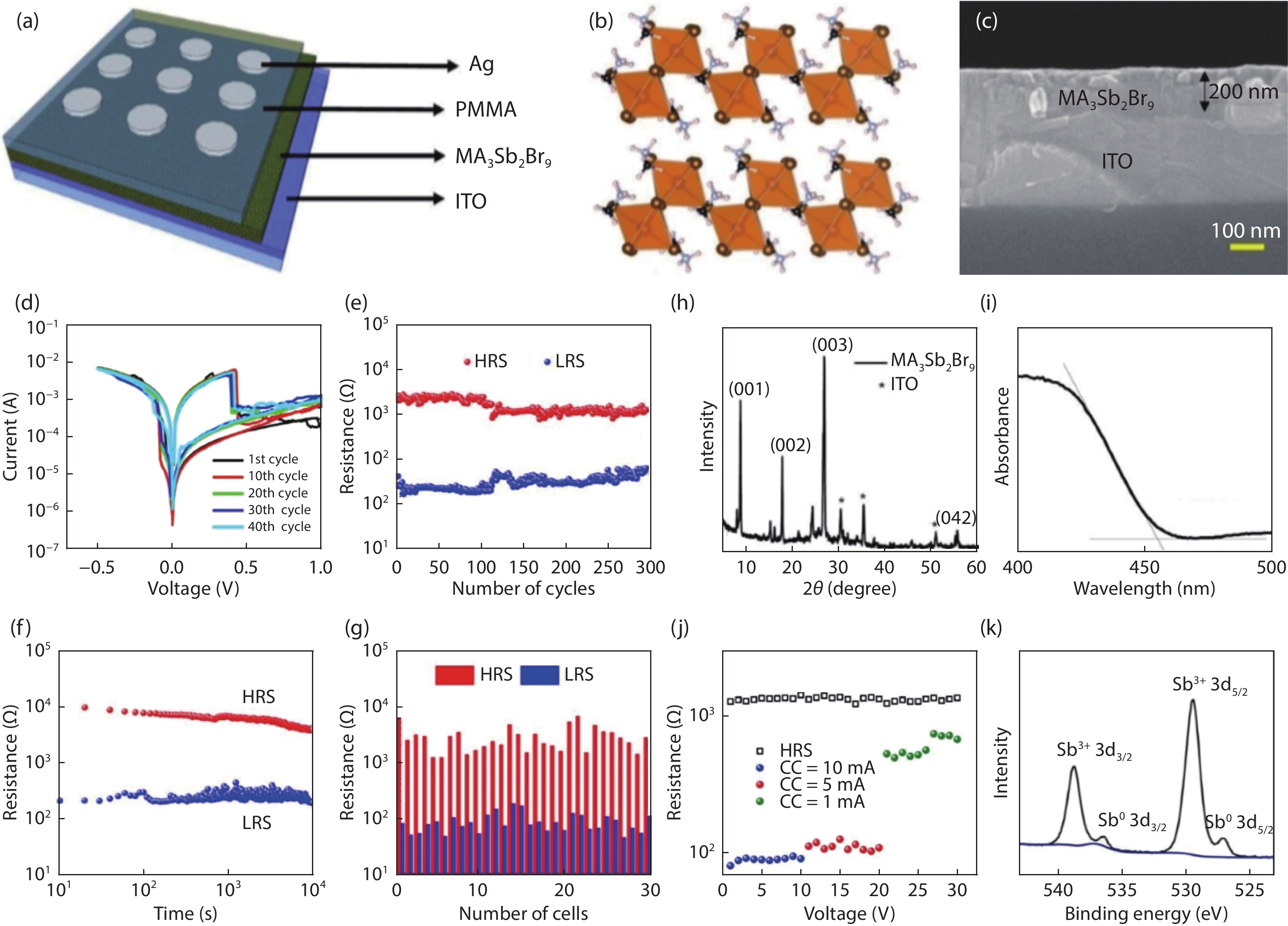
Yang J M, Choi E S, Kim S Y, et al. Perovskite-related (CH 3NH 3) 3Sb 2Br 9 for forming-free memristor and low-energy-consuming neuromorphic computing. Nanoscale, 2019, 11(13), 6453 doi: 10.1039/C8NR09918A |
| [87] |
Choi J, Park S, Lee J, et al. Organolead halide perovskites for low operating voltage multilevel resistive switching. Adv Mater, 2016, 28(31), 6562 doi: 10.1002/adma.201600859 |
| [88] |
Yang J M, Kim S G, Seo J Y, et al. 1D hexagonal HC(NH 2) 2PbI 3 for multilevel resistive switching nonvolatile memory. Adv Electron Mater, 2018, 4(9), 1800190 doi: 10.1002/aelm.201800190 |
| [89] |
Wang W, Xu J, Ma H, et al. Insertion of nanoscale AgInSbTe layer between the Ag electrode and the CH 3NH 3PbI 3 electrolyte layer enabling enhanced multilevel memory. ACS Appl Nano Mater, 2019, 2(1), 307 doi: 10.1021/acsanm.8b01928 |
| [90] |
Guan X, Hu W, Haque M A, et al. Light-responsive ion-redistribution-induced resistive switching in hybrid perovskite Schottky junctions. Adv Funct Mater, 2018, 28(3), 1704665 doi: 10.1002/adfm.201704665 |
| [91] |
Hwang B, Lee J S. A strategy to design high-density nanoscale devices utilizing vapor deposition of metal halide perovskite materials. Adv Mater, 2017, 29(29), 1701048 doi: 10.1002/adma.201701048 |
| [92] |
Zhu X, Lee J, Lu W D. Iodine vacancy redistribution in organic–inorganic halide perovskite films and resistive switching effects. Adv Mater, 2017, 29(29), 1700527 doi: 10.1002/adma.201700527 |
| [93] |
Lin C C, Tu B C, Lin C H, et al. Resistive switching mechanisms of V-doped SrZrO 3 memory films. IEEE Electron Device Lett, 2006, 27(9), 725 doi: 10.1109/LED.2006.880660 |
| [94] |
Yoo E, Lyu M, Yun J H, et al. Bifunctional resistive switching behavior in an organolead halide perovskite-based Ag/CH 3NH 3PbI 3– xCl x/FTO structure. J Mater Chem C, 2016, 4(33), 7824 doi: 10.1039/C6TC02503J |
| [95] |
Xiao Z, Huang J. Energy-efficient hybrid perovskite memristors and synaptic devices. Adv Electron Mater, 2016, 2(7), 1600100 doi: 10.1002/aelm.201600100 |
| [96] |
Yan X, Zhang L, Chen H, et al. Graphene oxide quantum dots based memristors with progressive conduction tuning for artificial synaptic learning. Adv Funct Mater, 2018, 28(40), 1803728 doi: 10.1002/adfm.201803728 |
| [97] |
Yan X, Pei Y, Chen H, et al. Self-assembled networked PbS distribution quantum dots for resistive switching and artificial synapse performance boost of memristors. Adv Mater, 2019, 31(7), 1805284 doi: 10.1002/adma.201805284 |
| [98] |
Xu W, Cho H, Kim Y H, et al. Organometal halide perovskite artificial synapses. Adv Mater, 2016, 28(28), 5916 doi: 10.1002/adma.201506363 |
| [99] |
Gholipour B, Bastock P, Craig C, et al. Amorphous metal-sulphide microfibers enable photonic synapses for brain-like computing. Adv Opt Mater, 2015, 3(5), 635 doi: 10.1002/adom.201400472 |
| [100] |
Pei K, Ren X, Zhou Z, et al. A high-performance optical memory array based on inhomogeneity of organic semiconductors. Adv Mater, 2018, 30(13), 1706647 doi: 10.1002/adma.201706647 |
| [101] |
Gorecki J, Apostolopoulos V, Ou J Y, et al. Optical gating of graphene on photoconductive Fe: LiNbO 3. ACS Nano, 2018, 12(6), 5940 doi: 10.1021/acsnano.8b02161 |
| [102] |
Shen Y, Harris N C, Skirlo S, et al. Deep learning with coherent nanophotonic circuits. Nat Photonics, 2017, 11(7), 441 doi: 10.1038/nphoton.2017.93 |
| [103] |
Dai S, Zhao Y, Wang Y, et al. Recent advances in transistor-based artificial synapses. Adv Funct Mater, 2019, 29(42), 1903700 doi: 10.1002/adfm.201903700 |
| [104] |
Wu Y, Wei Y, Huang Y, et al. Capping CsPbBr 3 with ZnO to improve performance and stability of perovskite memristors. Nano Res, 2017, 10(5), 1584 doi: 10.1007/s12274-016-1288-2 |
| [105] |
|
| [106] |
Liu X, Ramirez S, Pang P T, et al. Optogenetic stimulation of a hippocampal engram activates fear memory recall. Nature, 2012, 484(7394), 381 doi: 10.1038/nature11028 |
| [107] |
Zhu X, Lu W D. Optogenetics-inspired tunable synaptic functions in memristors. ACS Nano, 2018, 12(2), 1242 doi: 10.1021/acsnano.7b07317 |
| [108] |
|
| [109] |
Kramer R H, Mourot A, Adesnik H. Optogenetic pharmacology for control of native neuronal signaling proteins. Nat Neurosci, 2013, 16(7), 816 doi: 10.1038/nn.3424 |
| [110] |
Sun Y, Qian L, Xie D, et al. Photoelectric synaptic plasticity realized by 2D perovskite. Adv Funct Mater, 2019, 29(28), 1902538 doi: 10.1002/adfm.201902538 |
| [111] |
Jeon N J, Noh J H, Yang W S, et al. Compositional engineering of perovskite materials for high-performance solar cells. Nature, 2015, 517(7535), 476 doi: 10.1038/nature14133 |
| [112] |
Lim K G, Ahn S, Kim Y H, et al. Universal energy level tailoring of self-organized hole extraction layers in organic solar cells and organic-inorganic hybrid perovskite solar cells. Energy Environ Sci, 2016, 9(3), 932 doi: 10.1039/C5EE03560K |
| [113] |
Cheng C, Zhu C, Huang B, et al. Processing halide perovskite materials with semiconductor technology. Adv Mater Technol, 2019, 4(7), 1800729 doi: 10.1002/admt.201800729 |
| [114] |
Chamlagain B, Li Q, Ghimire N J, et al. Mobility improvement and temperature dependence in MoSe 2 field-effect transistors on parylene-C substrate. ACS Nano, 2014, 8(5), 5079 doi: 10.1021/nn501150r |
| [115] |
Skoblin G, Sun J, Yurgens A. Encapsulation of graphene in parylene. Appl Phys Lett, 2017, 110(5), 053504 doi: 10.1063/1.4975491 |
| [116] |
Kim M, Shah A, Li C, et al. Direct transfer of wafer-scale graphene films. 2D Mater, 2017, 4(3), 035004 doi: 10.1088/2053-1583/aa780d |
| [117] |
Yang X, Wu J, Liu T, et al. Patterned perovskites for optoelectronic applications. Small Methods, 2018, 2(10), 1800110 doi: 10.1002/smtd.201800110 |
| [118] |
Wang G, Li D, Cheng H C, et al. Wafer-scale growth of large arrays of perovskite microplate crystals for functional electronics and optoelectronics. Sci Adv, 2015, 1(9), e1500613 doi: 10.1126/sciadv.1500613 |
| [119] |
He X, Liu P, Zhang H, et al. Patterning multicolored microdisk laser arrays of cesium lead halide perovskite. Adv Mater, 2017, 29(12), 1604510 doi: 10.1002/adma.201604510 |
| [120] |
Zhao P, Kim B J, Ren X, et al. Antisolvent with an ultrawide processing window for the one-step fabrication of efficient and large-area perovskite solar cells. Adv Mater, 2018, 30(49), 1802763 doi: 10.1002/adma.201802763 |
| [121] |
Ren Y K, Ding X H, Wu Y H, et al. Temperature-assisted rapid nucleation: a facile method to optimize the film morphology for perovskite solar cells. J Mater Chem A, 2017, 5(38), 20327 doi: 10.1039/C7TA06334B |
| [122] |
Sanchez S, Christoph N, Grobety B, et al. Efficient and stable inorganic perovskite solar cells manufactured by pulsed flash infrared annealing. Adv Energy Mater, 2018, 8(30), 1802060 doi: 10.1002/aenm.201802060 |
| [123] |
Li D, Cheng H C, Wang Y, et al. The effect of thermal annealing on charge transport in organolead halide perovskite microplate field-effect transistors. Adv Mater, 2017, 29(4), 1601959 doi: 10.1002/adma.201601959 |
| [124] |
Wang Y, Li M, Li H, et al. Patterned wettability surface for competition-driving large-grained perovskite solar cells. Adv Energy Mater, 2019, 9(25), 1900838 doi: 10.1002/aenm.201900838 |


 DownLoad: