


1. Introduction
In the era of big data and artificial intelligence (AI), the demand for processing, memory and communication devices with higher speed, higher efficiency and lower power is becoming ever more urgent[1]. In the conventional von Neumann computing architecture, the memory and processing units are separated and combined together through the electrical interconnection, which lead to high energy consumption and low data transmission speed, and limits the further development of information communication system. Neurons in human brain connected by synapses can process and store great numbers of information simultaneously, which has provided an idea for overcoming the constraint of von Neumann system[2]. Memristive devices exhibit the synaptic behaviors, in which the resistance can be tune by continuous stimuli of voltage or current inputs, showing great potential as memory and logic devices for neuromorphic computing[3-10].
Non-volatile optical memory can directly sense, store, and process optical information in the same way as the neural network in the human visual system with light-tunable plasticity, which opens the door toward low-power artificial vision devices[11]. Two-dimensional (2D) materials have excellent optoelectronic properties, such as strong light-matter interaction[12], large surface-to-volume-ratio[13], reduced screening effect[14, 15] and flexibility. 2D materials open up numerous opportunities for non-volatile devices[16, 17], optical communication[18], imaging sensors[11, 19], logic gates[20], and neuromorphic systems[8]. Graphene modified with the light switchable molecules, azobenzenes, have shown light-driven conductance modulation[21]. However, the photocurrent rising time of ~1000 s is very slow due to the slow transformation of azobenzenes from trans to cis form. To date, there remains a significant challenge on achieving non-volatile optical memory. Herein, we construct a heterstructure geometry comprising graphene and CdSe QDs monolayer to achieve a non-volatile ORRAM device, in which the resistance can be tuned by visible light and exhibits light-tunable synaptic behaviours. The rising time is ~3 s under optical stimuli with a pulse width of 3 s. The optical storage time is up to ~450 s. This work provides a promising non-volatile unit toward neuromorphic systems.
2. Experiment
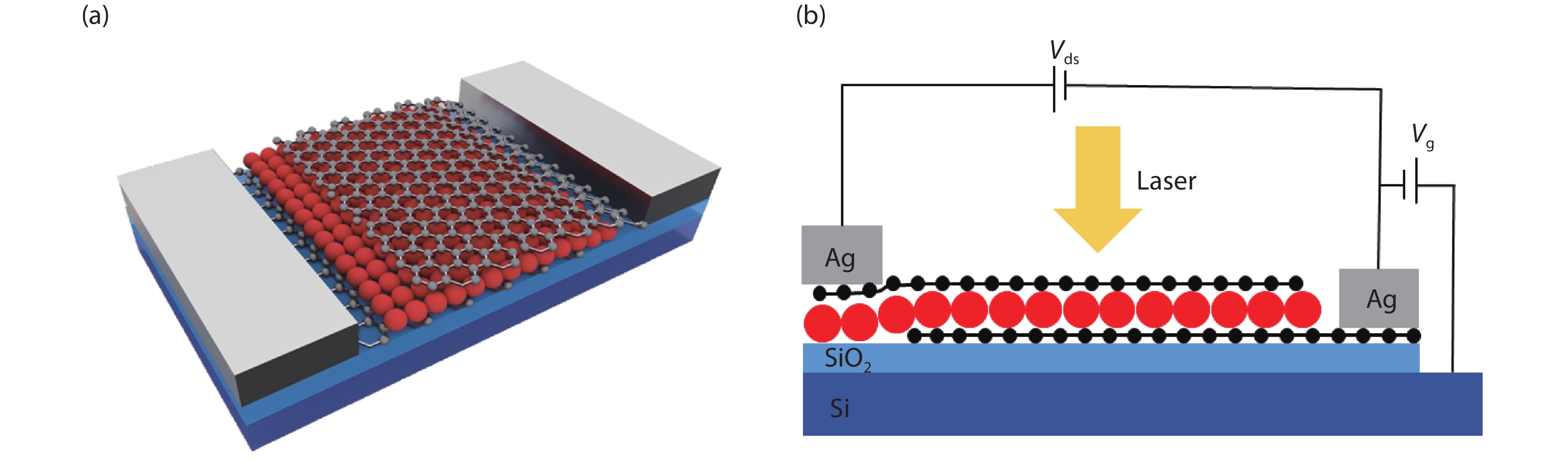
2.1 Device design
Fig. 1 shows a non-volatile optical memory with three-layer vertical heterostructure of graphene/QDs/graphene on Si/SiO2 substrate. In the two terminal symmetry ORRAM device, two monolayer graphene are used to sandwich a self-assembled monolayer CdSe QDs[22]. Silver electrodes are connected each piece of graphene (Fig. 1(b)). The CdSe QDs monolayer is used as a light absorption layer to generate photo-induced carriers under light excitation. Under bias voltage, the carriers separate to electrons and holes which disperse to the interface of CdSe QDs and graphene before recombination, in which graphene acts as highways for charge transfer.

 DownLoad:
2.2 Device fabrication
CVD-grown graphene was spin-coated with PMMA and wet-transferred onto Si/SiO2 (285 nm) substrate, then acetone was used to remove the PMMA. The monolayer CdSe quantum dot (QD) was prepared by dropping CdSe QDs solution (10 μL) onto the surface of acetonitrile solvent[22]. The self-assembled CdSe QDs monolayer was transferred onto the graphene substrates. Finally, the top graphene was covered on the CdSe QDs monolayer.
3. Results and discussion
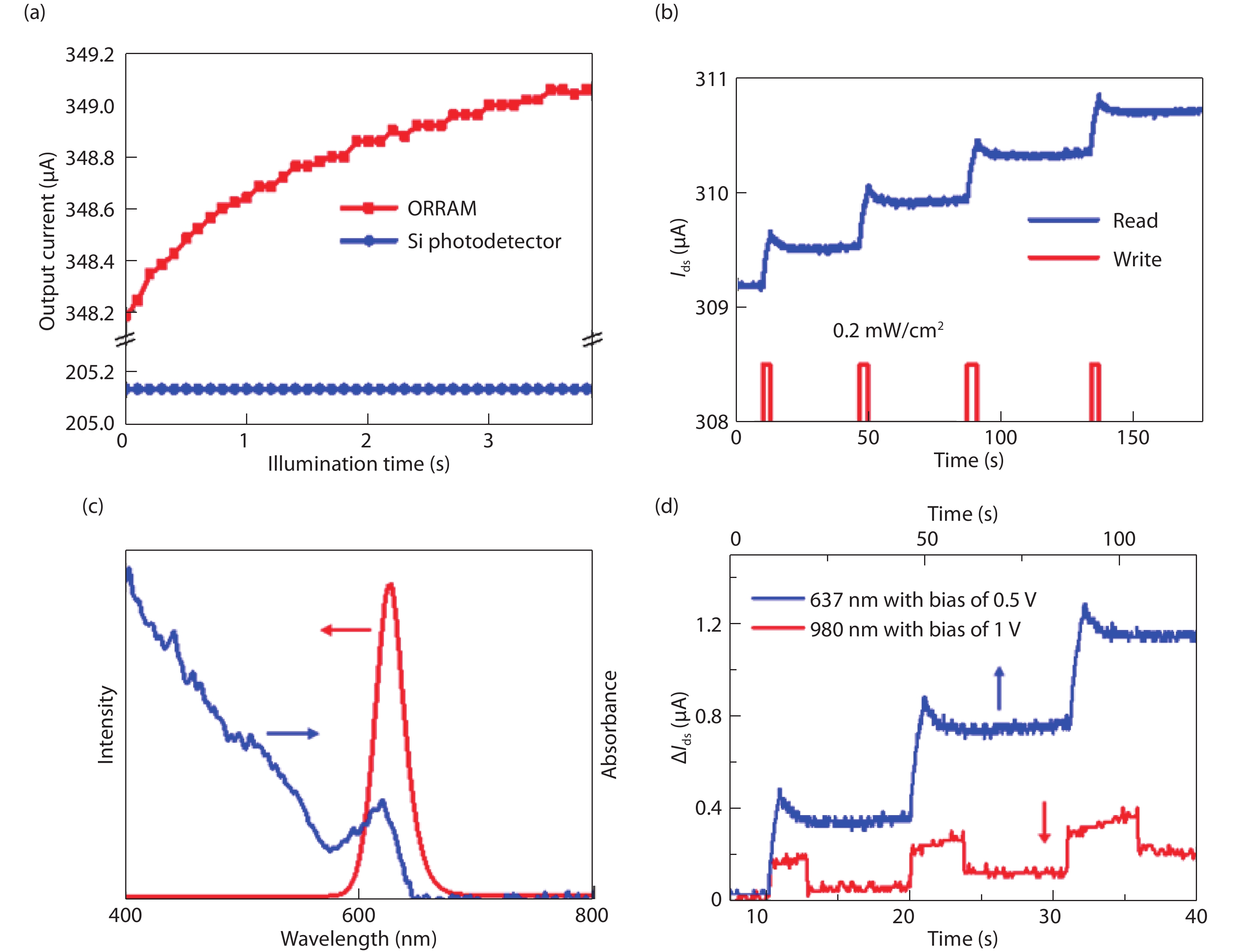
The resistance states of the ORRAM device can be tuned by optical stimulation. Displaying time-dependent and light-dosage-dependent behaviors opens the door to emulate the basic features of synaptic plasticity of the human brain. Fig. 2(a) shows the output current of a conventional commercial Si photodetector and our ORRAM synaptic device as a function of the illumination time. The photocurrent of Si photodetector remains constant. However, the output current of the ORRAM device is time-dependent, which increases with increasing illumination time. In many devices, a Schottky barrier may generate built-in electric field, which could drive the device[23]. But considering the symmetry of our device, the direction of the two layers of Schottky barrier is opposite, so we added bias voltage to drive the device. Fig. 2(b) shows the long-term plasticity under optical stimuli with pulse width of 3 s as a function of pulse number, the laser of 637 nm with 0.2 mW/cm2 is used as light source. The photocurrent states are preserved after removing the illumination. As the pulse numbers of optical stimulus increase, the output current increases with the same increase magnitude (~0.4 μA/pulse), Thus, the synaptic strengths of the ORRAM device increase significantly.

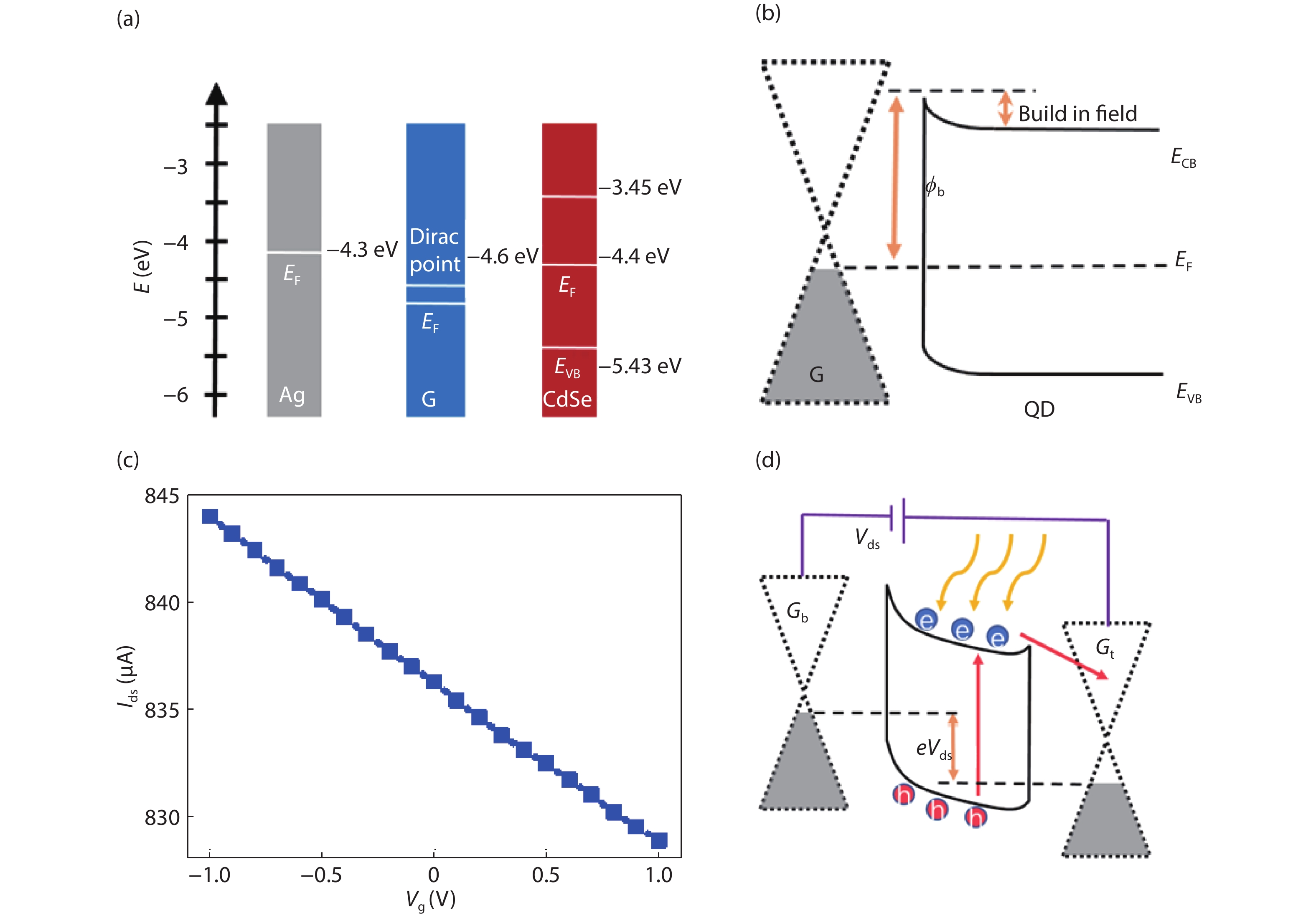
Fig. 2(c) shows the absorption and photoluminescence spectra of CdSe QDs. The PL peak of CdSe QDs is at ~627 nm and the absorption cutoff wavelength is at ~650 nm, indicating that an illumination wavelength should be smaller than 650 nm to ensure the excitation of QDs layer. In Fig. 2(d), we show the relative increase of the current of the device under three laser pulses. When a laser at 980 nm is used to illuminate the device, the photocurrent dramatically decreases compared with the value upon excitation by 637 nm laser, even both the bias and laser power is increased by 1 time, from 0.5 V and 0.2 mW/cm2 to 1 V and 0.5 mW/cm2. Because laser of 980 nm below the absorption cutoff wavelength of QDs, resulting in that the QDs layer does not have any light absorption. The photocurrent under 980 nm excitation arise from the broadband photoresponse of graphene[24]. Carriers are generated after graphene absorbs the photon energy, and could disperse under the bias voltage in the device. The energy band offsets of Ag, graphene and CdSe QDs are shown in Fig. 3(a). The Fermi level of intrinsic graphene and CdSe QDs is about –4.6 and –4.4 eV, respectively. Due to the doping of water vapor and other substances in the air, graphene often shows a p-type doping state, so the Fermi level is lower than the position of Dirac point[25]. The edge of the conduction band (ECB) and valence band (EVB) of the CdSe QDs are located at –3.45 and –5.43 eV, respectively[26]. Because the Fermi level of the CdSe QDs is higher than that of graphene, the band edge (CB and VB) of CdSe QDs thus bend downward at the interface of graphene and CdSe QDs, leading to the formation of the Schottky barrier (Φb), as shown in Fig. 3(b). Fig. 3(c) displays the gate dependence of current (Ids) without light illumination under the bias of 1 V. However, it should be noted that this bias dependence of current is measured after the device has been exposed to light for a long time, thus many photogenerated carriers gather in the device, resulting in an increasing absolute current value. When a positive gate voltage is applied (Vg > 0), which induce an electron injection, the Ids decrease. In contrast, when we apply Vg < 0, the Gb give rise to a hole injection and the Ids increase. This phenomenon validates than a p-type doping can improve the performance of the ORRAM device.

Previous studies have reported defect-induced non-volatile behaviors[27-30], in which charges are trapped by defects like oxygen vacancies, but this could not explain the multi-level storage states of our device. We anticipate that the interfacial Schottky barrier gives rise to the synaptic behaviors. The electrons in CdSe QDs jump to the conduction band from the valence band upon light excitation and leave holes in the valence band. The electrons and holes move in the opposite direction along the tilted band edges arising from the bias (Fig. 3(d)). The carriers are trapped and accumulate with high densities at the interface of graphene and quantum dots due to the Schottky barrier. Subsequently, the carriers tunnel from the band edges of CdSe QDs to graphene, giving rise to a increasing photocurrent and synaptic behaviors. The non-volatile optical storage time depend on the decay time of the accumulated carriers. Therefore, the output current is dependent on the pulse number of optical stimulus and light dosages.
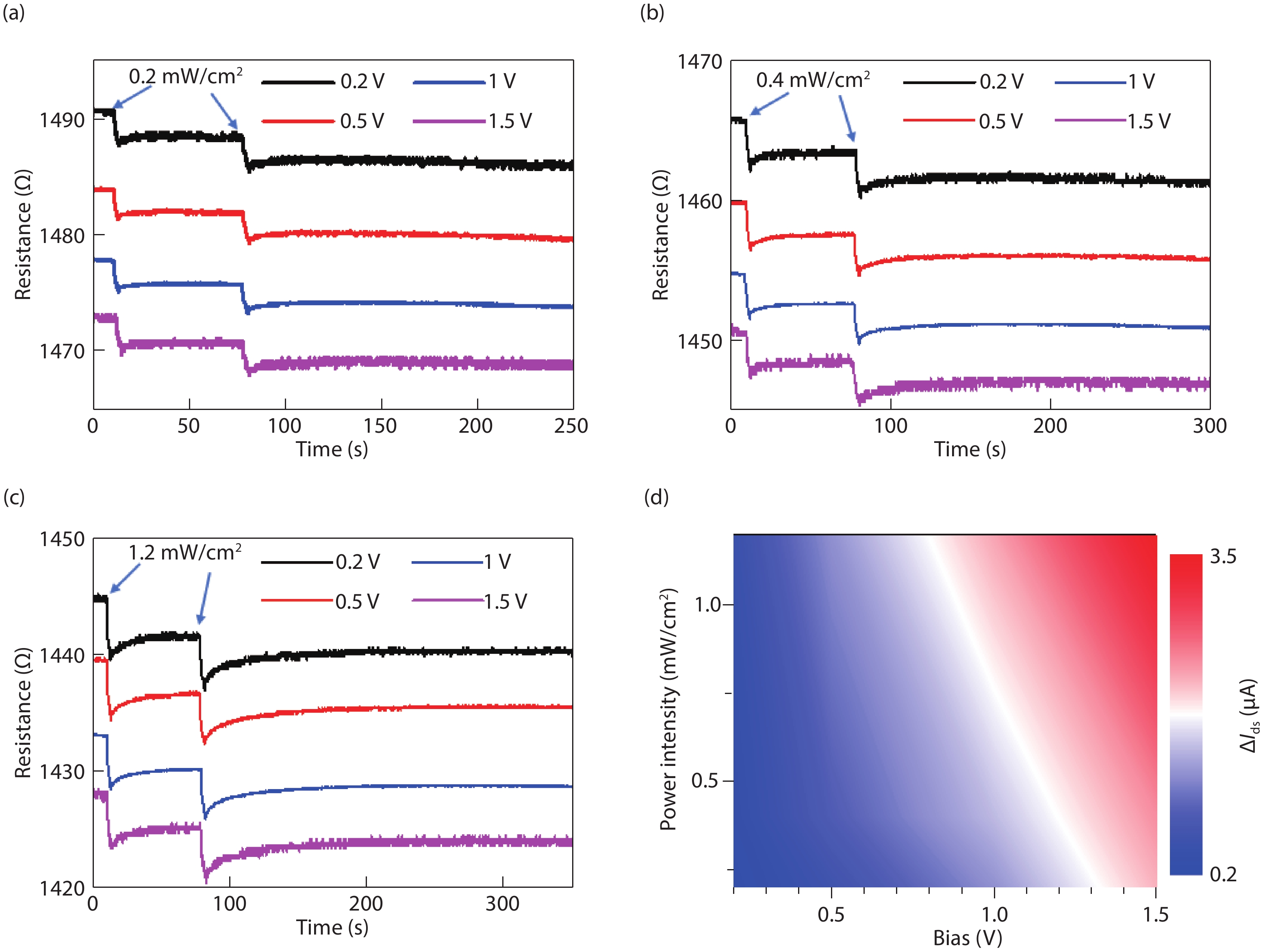
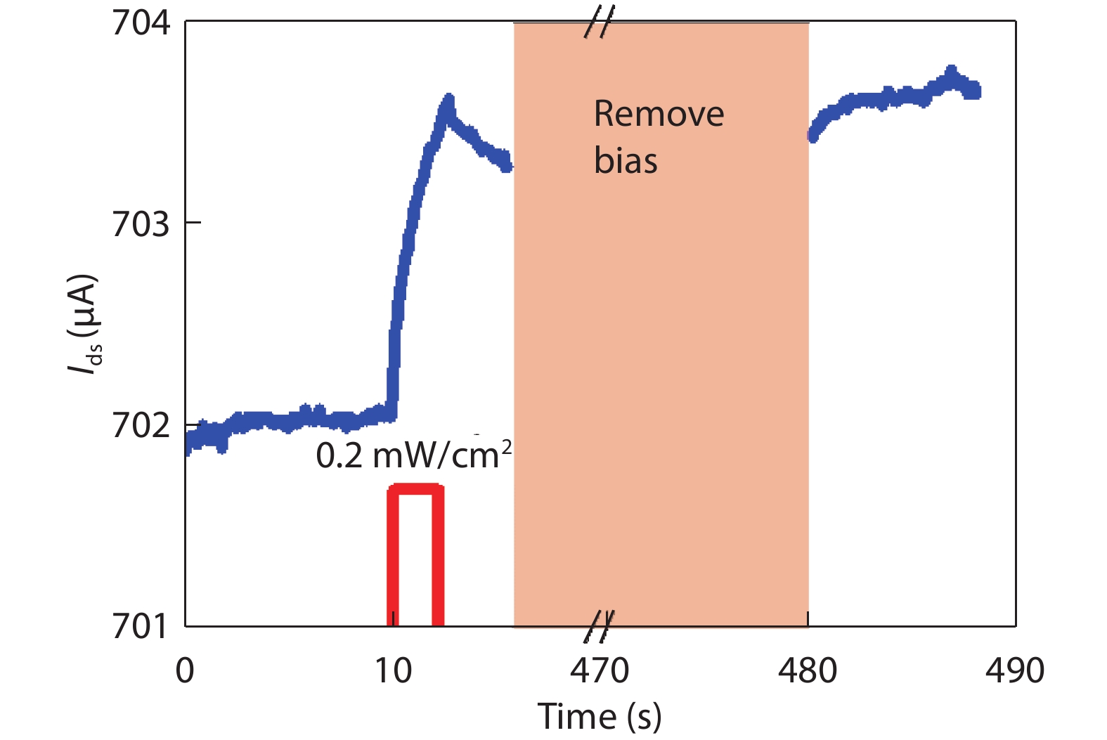
To further understand the mechanism, the effects of light intensity and bias on the synaptic behaviors are studied. Striking capacities of multi-level storage are observed (Figs. 4(a) and 4(b)). The increased laser power can induce increases of photogenerated carriers gathering at the interface states due to the Schottky barrier, while the increased bias voltage accelerates the carrier migration and tunneling. Thus, the output current and synaptic strengths of the ORRAM devices increase with increasing laser power and bias voltages, consistent with the mechanism in Fig. 3(d). Fig. 4(d) shows the corresponding 2D mapping of the ΔIds, ΔIds = IL – I0, where IL and I0 are the output current in the presence and absence of a pulsed laser illumination, respectively. The non-volatile resistance retention time of the ORRAM device is up to ~450 s after removing bias voltage (Fig. 5), which further confirm the stable long-term plasticity behaviors. The synaptic behaviors of the ORRAM devices can be tuned by light dosage and bias voltages, which allow us to design different strategies to emulate the features of synaptic plasticity to achieve the learning and memory functions of the human brain.


4. Conclusion
In this work, we have proposed and demonstrated a non-volatile optical memory and synaptic behaviors in a three-layer vertical heterostructure of graphene/CdSe QDs/graphene. The ORRAM device exhibits multi-level memory capability and long storage time. The Schottky barrier between graphene and CdSe QDs introduces interface states to localize photo-induced carriers, leading to non-volatile optical memory. Furthermore, the low laser power and bias voltage reduce the energy consumption. This work shows great potential to apply 2D heterostructures in non-volatile optical memory and artificial neural networks.
Acknowledgements
We acknowledge financial support from National Science Foundation of China (51602040, 51872039), Science and Technology Program of Sichuan (M112018JY0025) and Scientific Research Foundation for New Teachers of UESTC (A03013023601007).
 DownLoad:


 DownLoad:


