


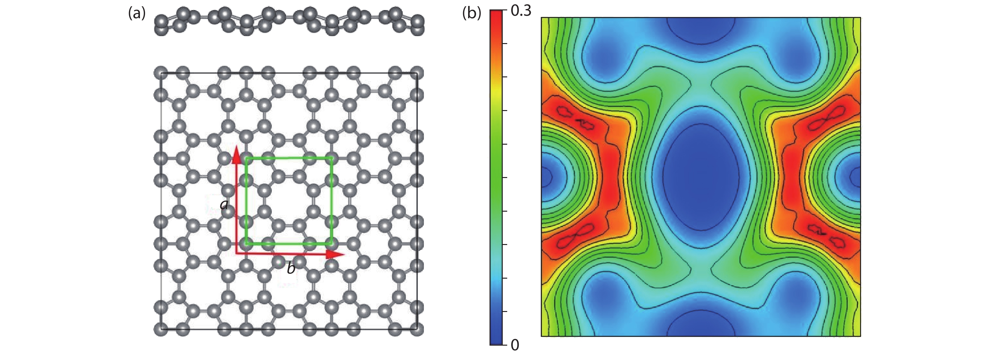
Fig. 1.
(Color online) (a) The crystalline structures and (b) 2D charge density difference plot of C568. The square unit-cell marked in green line, where a and b represent unitcell vectors.
ARTICLES
Qiang Gao1, 2, Hasan Sahin3 and Jun Kang2,
Corresponding author: Jun Kang, Email: jkang@csrc.ac.cn
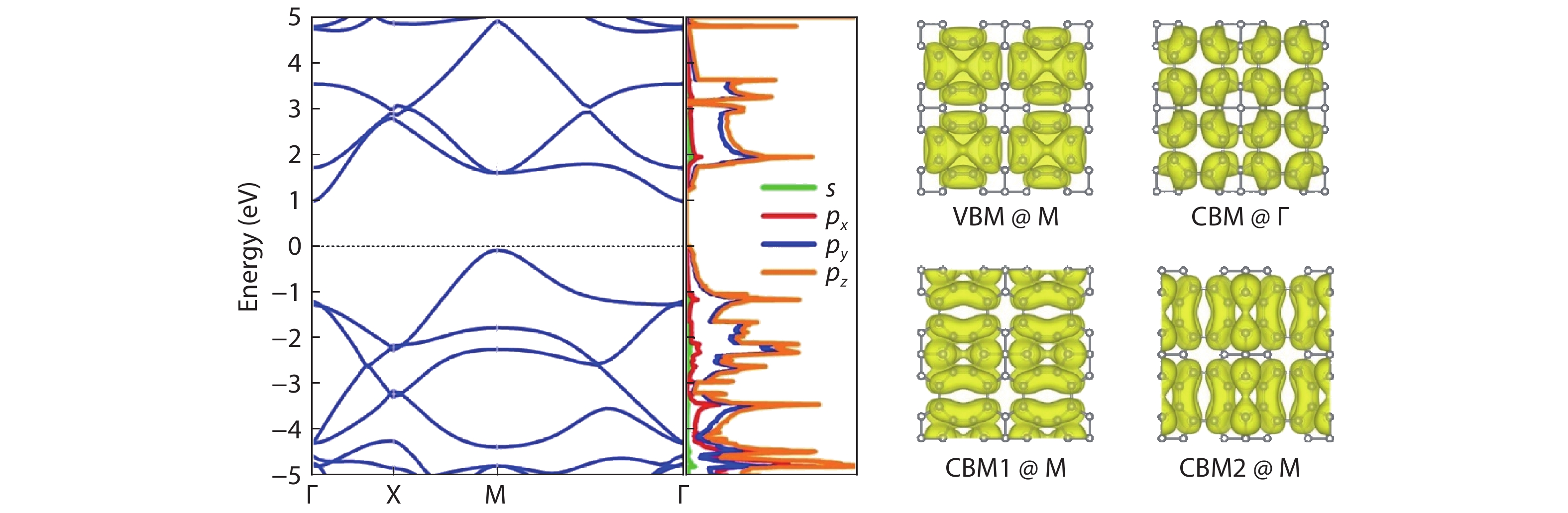
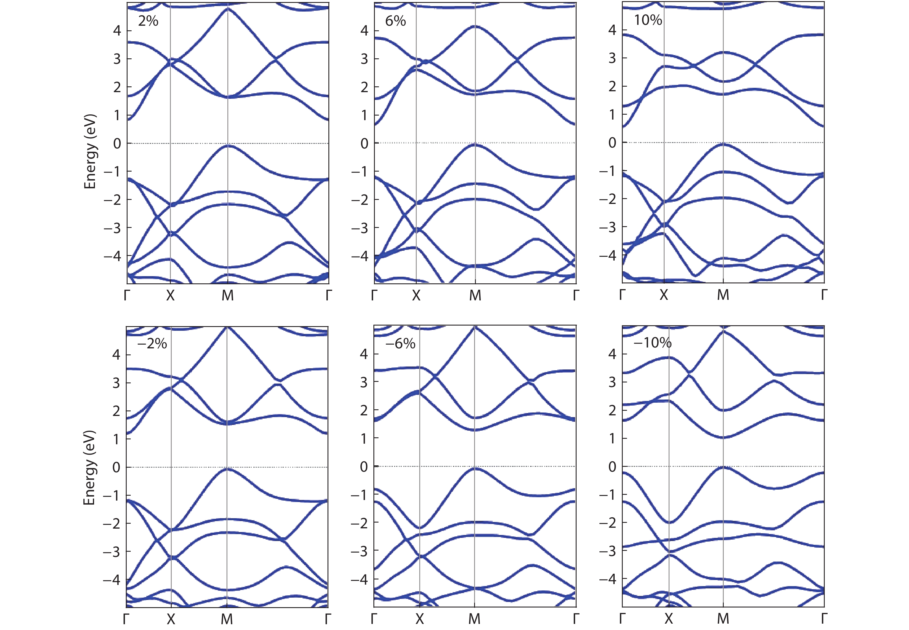
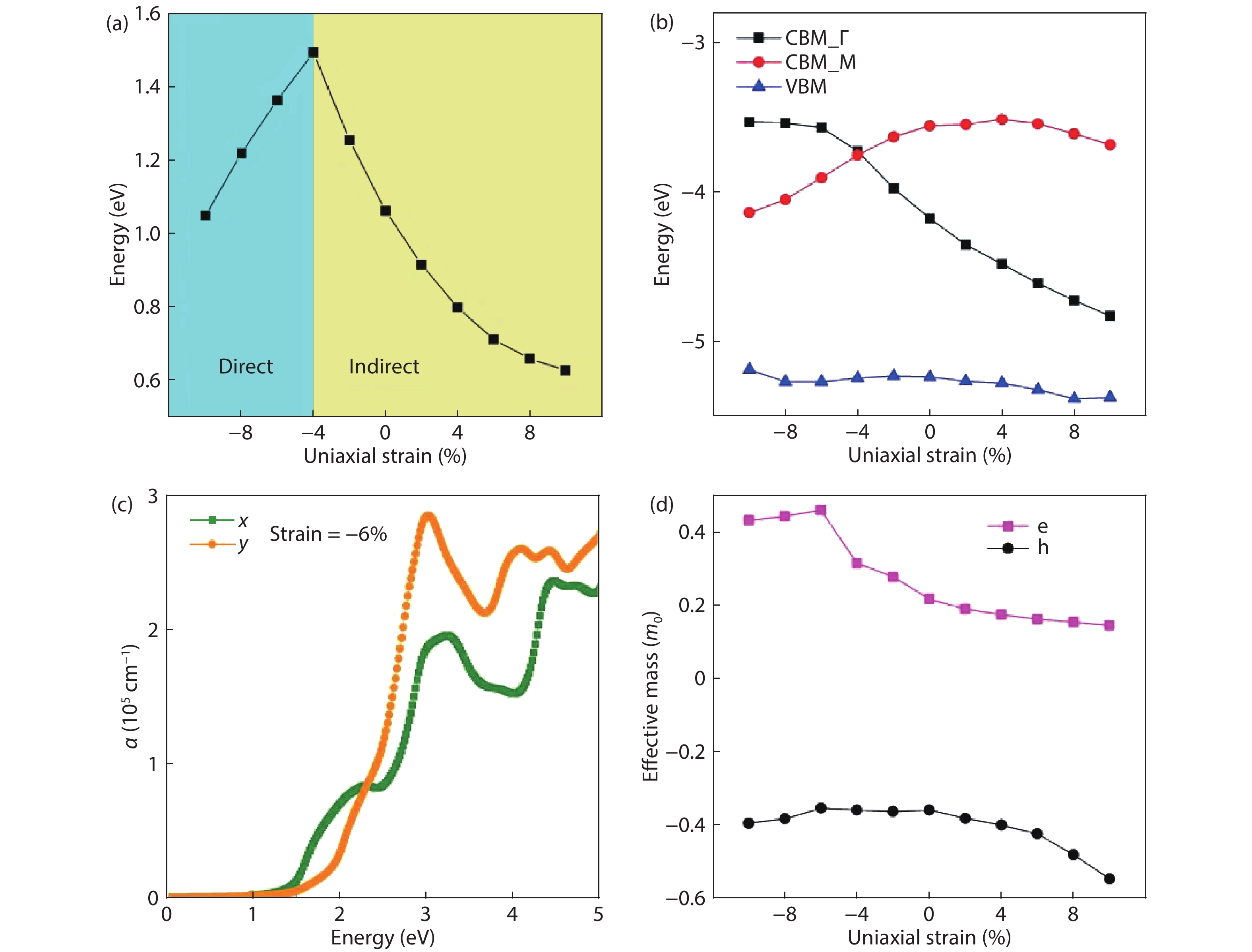
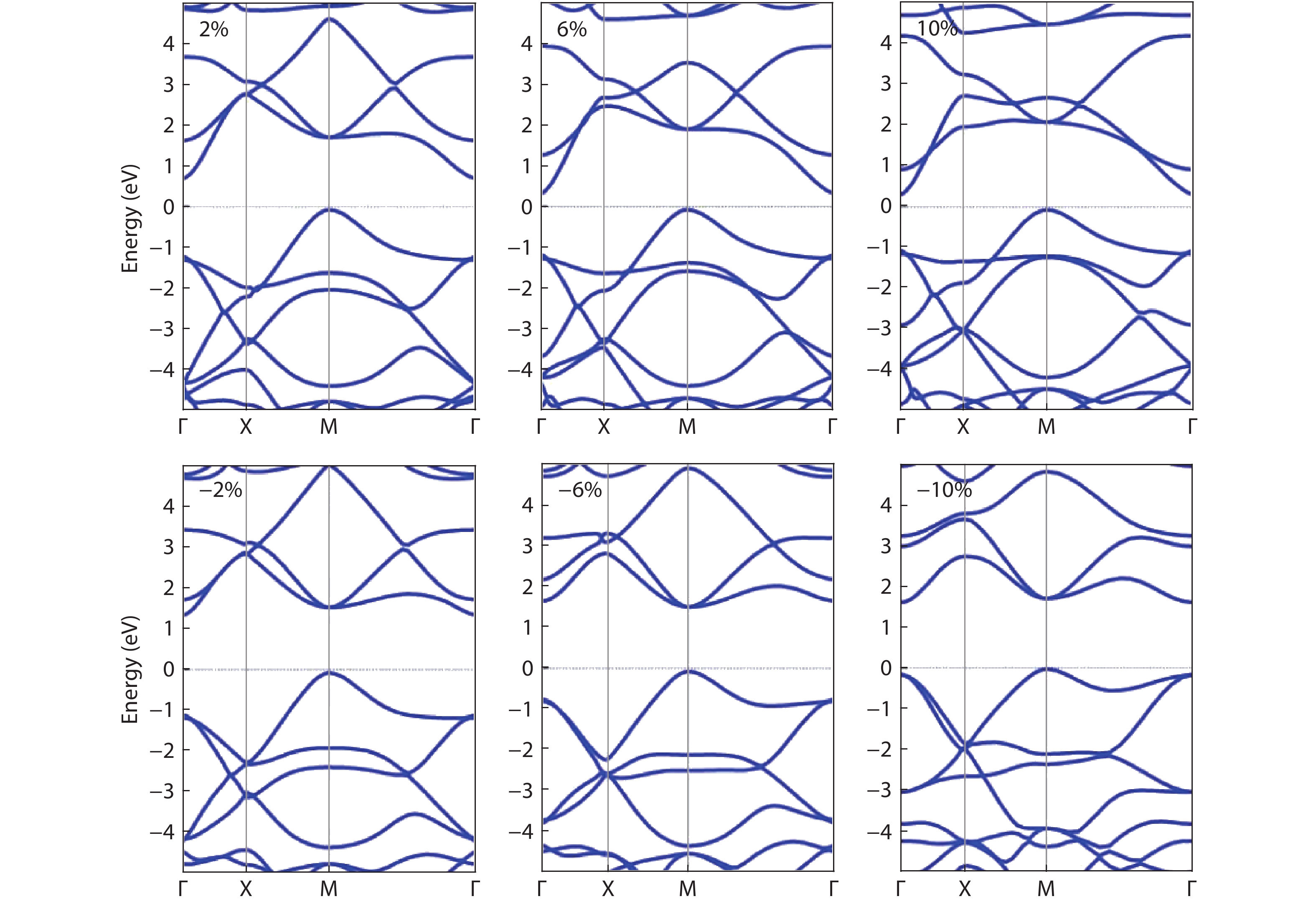
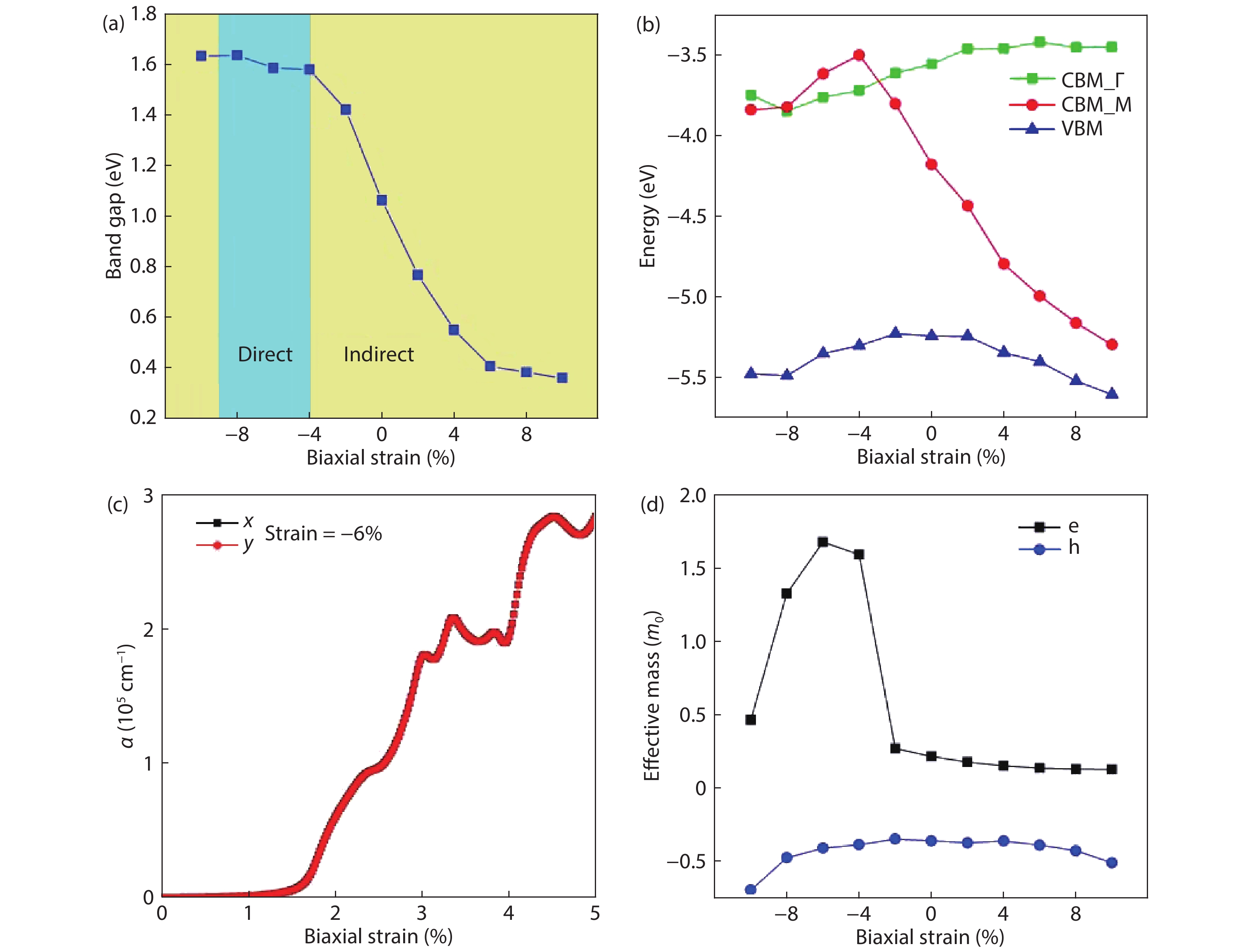
Abstract: Recently, C568 has emerged as a new carbon allotrope, which shows semiconducting properties with a band gap around 1 eV and has attracted much attention. In this work, the external strain effects on the electronic properties of C568 have been studied theoretically through first-principle calculations. The numerical results show that while in-plane uniaxial and biaxial strains both reduces the band gap of C568 in case of tensile strain, their effects are quite different in the case of compressive strain. With increasing compressive uniaxial strain, the band gap of C568 first increases, and then dramatically decreases. In contrast, the application of compressive biaxial strain up to –10% only leads to a slight increase of band gap. Moreover, an indirect-to-direct gap transition can be realized under both types of compressive strain. The results also show that the optical anisotropy of C568 can be induced under uniaxial strain, while biaxial strain does not cause such an effect. These results indicate good strain tunability of the band structure of C568, which could be helpful for the design and optimization of C568-based nanodevices.
Key words: 2D C568, monoelemental 2D atomic crystalline materials, strain effects, electronic structures
| [1] |
Novoselov K S, Geim A K, Morozov S V, et al. Two-dimensional gas of massless Dirac fermions in graphene. Nature, 2005, 438, 197 doi: 10.1038/nature04233
|
| [2] |
Ferrari A C, Meyer J C, Scardaci V, et al. Raman spectrum of graphene and graphene layers. Phys Rev Lett, 2006, 97, 187401 doi: 10.1103/PhysRevLett.97.187401
|
| [3] |
Geim A K, Novoselov K S. The rise of graphene. Nat Mater, 2007, 6, 183 doi: 10.1038/nmat1849
|
| [4] |
Han M Y, Özyilmaz B, Zhang Y B, et al. Energy band-gap engineering of graphene nanoribbons. Phys Rev Lett, 2007, 98, 206805 doi: 10.1103/PhysRevLett.98.206805
|
| [5] |
Zhu W J, Neumayer D, Perebeinos V, et al. Silicon nitride gate dielectrics and band gap engineering in graphene layers. Nano Lett, 2010, 10, 3572 doi: 10.1021/nl101832y
|
| [6] |
Mak K F, Lee C, Hone J, et al. Atomically thin MoS2: A new direct-gap semiconductor. Phys Rev Lett, 2010, 105, 136805 doi: 10.1103/PhysRevLett.105.136805
|
| [7] |
Radisavljevic B, Radenovic A, Brivio J, et al. Single-layer MoS2 transistors. Nat Nanotechnol, 2011, 6, 147 doi: 10.1038/nnano.2010.279
|
| [8] |
Mak K F, He K, Shan J, et al. Control of valley polarization in monolayer MoS2 by optical helicity. Nat Nanotechnol, 2012, 7, 494 doi: 10.1038/nnano.2012.96
|
| [9] |
Li L K, Yu Y J, Ye G J, et al. Black phosphorus field-effect transistors. Nat Nanotechnol, 2014, 9, 372 doi: 10.1038/nnano.2014.35
|
| [10] |
Reich E S. Phosphorene excites materials scientists. Nature, 2014, 506, 19 doi: 10.1038/506019a
|
| [11] |
Fiori G, Bonaccorso F, Iannaccone G, et al. Erratum: Electronics based on two-dimensional materials. Nat Nanotechnol, 2014, 9, 1063 doi: 10.1038/nnano.2014.283
|
| [12] |
Xu M S, Liang T, Shi M M, et al. Graphene-like two-dimensional materials. Chem Rev, 2013, 113, 3766 doi: 10.1021/cr300263a
|
| [13] |
Vogt P, de Padova P, Quaresima C, et al. Silicene: Compelling experimental evidence for graphenelike two-dimensional silicon. Phys Rev Lett, 2012, 108, 155501 doi: 10.1103/PhysRevLett.108.155501
|
| [14] |
Dávila M E, Xian L, Cahangirov S, et al. Germanene: A novel two-dimensional germanium allotrope akin to graphene and silicene. New J Phys, 2014, 16, 095002 doi: 10.1088/1367-2630/16/9/095002
|
| [15] |
Zhu F F, Chen W J, Xu Y, et al. Epitaxial growth of two-dimensional stanene. Nat Mater, 2015, 14, 1020 doi: 10.1038/nmat4384
|
| [16] |
Zhu Z, Cai X, Yi S, et al. Multivalency-driven formation of Te-based monolayer materials: A combined first-principles and experimental study. Phys Rev Lett, 2017, 119, 106101 doi: 10.1103/PhysRevLett.119.106101
|
| [17] |
Wang Z H, Zhou X F, Zhang X M, et al. Phagraphene: A low-energy graphene allotrope composed of 5-6-7 carbon rings with distorted Dirac cones. Nano Lett, 2015, 15, 6182 doi: 10.1021/acs.nanolett.5b02512
|
| [18] |
Liu Y, Wang G, Huang Q S, et al. Structural and electronic properties of T graphene: A two-dimensional carbon allotrope with tetrarings. Phys Rev Lett, 2012, 108, 225505 doi: 10.1103/PhysRevLett.108.225505
|
| [19] |
Baughman R H, Eckhardt H, Kertesz M. Structure-property predictions for new planar forms of carbon: Layered phases containing sp2 and sp atoms. J Chem Phys, 1987, 87, 6687 doi: 10.1063/1.453405
|
| [20] |
Narita N, Nagai S, Suzuki S, et al. Optimized geometries and electronic structures of graphyne and its family. Phys Rev B, 1998, 58, 11009 doi: 10.1103/PhysRevB.58.11009
|
| [21] |
Li G X, Li Y L, Liu H B, et al. Architecture of graphdiyne nanoscale films. Chem Commun, 2010, 46, 3256 doi: 10.1039/b922733d
|
| [22] |
Long M Q, Tang L, Wang D, et al. Electronic structure and carrier mobility in graphdiyne sheet and nanoribbons: Theoretical predictions. ACS Nano, 2011, 5, 2593 doi: 10.1021/nn102472s
|
| [23] |
Song Q, Wang B, Deng K, et al. Graphenylene, a unique two-dimensional carbon network with nondelocalized cyclohexatriene units. J Mater Chem C, 2013, 1, 38 doi: 10.1039/C2TC00006G
|
| [24] |
Zhang S H, Zhou J, Wang Q, et al. Penta-graphene: A new carbon allotrope. PNAS, 2015, 112, 2372 doi: 10.1073/pnas.1416591112
|
| [25] |
Ram B, Mizuseki H. Tetrahexcarbon: A two-dimensional allotrope of carbon. Carbon, 2018, 137, 266 doi: 10.1016/j.carbon.2018.05.034
|
| [26] |
Ram B, Mizuseki H. C568: A new two-dimensional sp2–sp3 hybridized allotrope of carbon. Carbon, 2020, 158, 827 doi: 10.1016/j.carbon.2019.11.062
|
| [27] |
Kresse G, Furthmüller J. Efficient iterative schemes for ab initio total-energy calculations using a plane-wave basis set. Phys Rev B, 1996, 54, 11169 doi: 10.1103/PhysRevB.54.11169
|
| [28] |
Perdew J P, Burke K, Ernzerhof M. Generalized gradient approximation made simple. Phys Rev Lett, 1996, 77, 3865 doi: 10.1103/PhysRevLett.77.3865
|
| [29] |
Blöchl P E. Projector augmented-wave method. Phys Rev B, 1994, 50, 17953 doi: 10.1103/PhysRevB.50.17953
|
| [30] |
Heyd J, Peralta J E, Scuseria G E, et al. Energy band gaps and lattice parameters evaluated with the Heyd–Scuseria–Ernzerhof screened hybrid functional. J Chem Phys, 2005, 123, 174101 doi: 10.1063/1.2085170
|
| [31] |
Monkhorst H J, Pack J D. Special points for Brillouin-zone integrations. Phys Rev B, 1976, 13, 5188 doi: 10.1103/PhysRevB.13.5188
|
| [32] |
Wang V, Xu N, Liu J C, et al. VASPKIT: A pre- and post-processing program for VASP code. arXiv: 1908.08269, 2019
|
| [33] |
Kang J, Tongay S, Zhou J, et al. Band offsets and heterostructures of two-dimensional semiconductors. Appl Phys Lett, 2013, 102, 012111 doi: 10.1063/1.4774090
|
| [34] |
Wang X, Li Y, Huang L, et al. Short-wave near-infrared linear dichroism of two-dimensional germanium selenide. J Am Chem Soc, 2017, 139, 14976 doi: 10.1021/jacs.7b06314
|
| [35] |
Zhao K, Wei Z M, Jiang X W. Polarized photodetectors based on two-dimensional semiconductors. Sci China Phys Mech Astron, 2019, 63, 1 doi: 10.1007/s11433-019-1461-2
|
| [36] |
Li Z, Lv Y, Ren L, et al. Efficient strain modulation of 2D materials via polymer encapsulation. Nat Commun, 2020, 11, 1151 doi: 10.1038/s41467-020-15023-3
|
| [37] |
Akinwande D, Petrone N, Hone J. Two-dimensional flexible nanoelectronics. Nat Commun, 2014, 5, 5678 doi: 10.1038/ncomms6678
|
| [38] |
Das S, Gulotty R, Sumant A V, et al. All two-dimensional, flexible, transparent, and thinnest thin film transistor. Nano Lett, 2014, 14, 2861 doi: 10.1021/nl5009037
|


Article views: 4778 Times PDF downloads: 61 Times Cited by: 0 Times
Received: 29 May 2020 Revised: 24 June 2020 Online: Accepted Manuscript: 06 July 2020Uncorrected proof: 10 July 2020Published: 04 August 2020
| Citation: |
Qiang Gao, Hasan Sahin, Jun Kang. Strain tunable band structure of a new 2D carbon allotrope C568[J]. Journal of Semiconductors, 2020, 41(8): 082005. doi: 10.1088/1674-4926/41/8/082005
****
Q Gao, H Sahin, J Kang, Strain tunable band structure of a new 2D carbon allotrope C568[J]. J. Semicond., 2020, 41(8): 082005. doi: 10.1088/1674-4926/41/8/082005.

|
| [1] |
Novoselov K S, Geim A K, Morozov S V, et al. Two-dimensional gas of massless Dirac fermions in graphene. Nature, 2005, 438, 197 doi: 10.1038/nature04233
|
| [2] |
Ferrari A C, Meyer J C, Scardaci V, et al. Raman spectrum of graphene and graphene layers. Phys Rev Lett, 2006, 97, 187401 doi: 10.1103/PhysRevLett.97.187401
|
| [3] |
Geim A K, Novoselov K S. The rise of graphene. Nat Mater, 2007, 6, 183 doi: 10.1038/nmat1849
|
| [4] |
Han M Y, Özyilmaz B, Zhang Y B, et al. Energy band-gap engineering of graphene nanoribbons. Phys Rev Lett, 2007, 98, 206805 doi: 10.1103/PhysRevLett.98.206805
|
| [5] |
Zhu W J, Neumayer D, Perebeinos V, et al. Silicon nitride gate dielectrics and band gap engineering in graphene layers. Nano Lett, 2010, 10, 3572 doi: 10.1021/nl101832y
|
| [6] |
Mak K F, Lee C, Hone J, et al. Atomically thin MoS2: A new direct-gap semiconductor. Phys Rev Lett, 2010, 105, 136805 doi: 10.1103/PhysRevLett.105.136805
|
| [7] |
Radisavljevic B, Radenovic A, Brivio J, et al. Single-layer MoS2 transistors. Nat Nanotechnol, 2011, 6, 147 doi: 10.1038/nnano.2010.279
|
| [8] |
Mak K F, He K, Shan J, et al. Control of valley polarization in monolayer MoS2 by optical helicity. Nat Nanotechnol, 2012, 7, 494 doi: 10.1038/nnano.2012.96
|
| [9] |
Li L K, Yu Y J, Ye G J, et al. Black phosphorus field-effect transistors. Nat Nanotechnol, 2014, 9, 372 doi: 10.1038/nnano.2014.35
|
| [10] |
Reich E S. Phosphorene excites materials scientists. Nature, 2014, 506, 19 doi: 10.1038/506019a
|
| [11] |
Fiori G, Bonaccorso F, Iannaccone G, et al. Erratum: Electronics based on two-dimensional materials. Nat Nanotechnol, 2014, 9, 1063 doi: 10.1038/nnano.2014.283
|
| [12] |
Xu M S, Liang T, Shi M M, et al. Graphene-like two-dimensional materials. Chem Rev, 2013, 113, 3766 doi: 10.1021/cr300263a
|
| [13] |
Vogt P, de Padova P, Quaresima C, et al. Silicene: Compelling experimental evidence for graphenelike two-dimensional silicon. Phys Rev Lett, 2012, 108, 155501 doi: 10.1103/PhysRevLett.108.155501
|
| [14] |
Dávila M E, Xian L, Cahangirov S, et al. Germanene: A novel two-dimensional germanium allotrope akin to graphene and silicene. New J Phys, 2014, 16, 095002 doi: 10.1088/1367-2630/16/9/095002
|
| [15] |
Zhu F F, Chen W J, Xu Y, et al. Epitaxial growth of two-dimensional stanene. Nat Mater, 2015, 14, 1020 doi: 10.1038/nmat4384
|
| [16] |
Zhu Z, Cai X, Yi S, et al. Multivalency-driven formation of Te-based monolayer materials: A combined first-principles and experimental study. Phys Rev Lett, 2017, 119, 106101 doi: 10.1103/PhysRevLett.119.106101
|
| [17] |
Wang Z H, Zhou X F, Zhang X M, et al. Phagraphene: A low-energy graphene allotrope composed of 5-6-7 carbon rings with distorted Dirac cones. Nano Lett, 2015, 15, 6182 doi: 10.1021/acs.nanolett.5b02512
|
| [18] |
Liu Y, Wang G, Huang Q S, et al. Structural and electronic properties of T graphene: A two-dimensional carbon allotrope with tetrarings. Phys Rev Lett, 2012, 108, 225505 doi: 10.1103/PhysRevLett.108.225505
|
| [19] |
Baughman R H, Eckhardt H, Kertesz M. Structure-property predictions for new planar forms of carbon: Layered phases containing sp2 and sp atoms. J Chem Phys, 1987, 87, 6687 doi: 10.1063/1.453405
|
| [20] |
Narita N, Nagai S, Suzuki S, et al. Optimized geometries and electronic structures of graphyne and its family. Phys Rev B, 1998, 58, 11009 doi: 10.1103/PhysRevB.58.11009
|
| [21] |
Li G X, Li Y L, Liu H B, et al. Architecture of graphdiyne nanoscale films. Chem Commun, 2010, 46, 3256 doi: 10.1039/b922733d
|
| [22] |
Long M Q, Tang L, Wang D, et al. Electronic structure and carrier mobility in graphdiyne sheet and nanoribbons: Theoretical predictions. ACS Nano, 2011, 5, 2593 doi: 10.1021/nn102472s
|
| [23] |
Song Q, Wang B, Deng K, et al. Graphenylene, a unique two-dimensional carbon network with nondelocalized cyclohexatriene units. J Mater Chem C, 2013, 1, 38 doi: 10.1039/C2TC00006G
|
| [24] |
Zhang S H, Zhou J, Wang Q, et al. Penta-graphene: A new carbon allotrope. PNAS, 2015, 112, 2372 doi: 10.1073/pnas.1416591112
|
| [25] |
Ram B, Mizuseki H. Tetrahexcarbon: A two-dimensional allotrope of carbon. Carbon, 2018, 137, 266 doi: 10.1016/j.carbon.2018.05.034
|
| [26] |
Ram B, Mizuseki H. C568: A new two-dimensional sp2–sp3 hybridized allotrope of carbon. Carbon, 2020, 158, 827 doi: 10.1016/j.carbon.2019.11.062
|
| [27] |
Kresse G, Furthmüller J. Efficient iterative schemes for ab initio total-energy calculations using a plane-wave basis set. Phys Rev B, 1996, 54, 11169 doi: 10.1103/PhysRevB.54.11169
|
| [28] |
Perdew J P, Burke K, Ernzerhof M. Generalized gradient approximation made simple. Phys Rev Lett, 1996, 77, 3865 doi: 10.1103/PhysRevLett.77.3865
|
| [29] |
Blöchl P E. Projector augmented-wave method. Phys Rev B, 1994, 50, 17953 doi: 10.1103/PhysRevB.50.17953
|
| [30] |
Heyd J, Peralta J E, Scuseria G E, et al. Energy band gaps and lattice parameters evaluated with the Heyd–Scuseria–Ernzerhof screened hybrid functional. J Chem Phys, 2005, 123, 174101 doi: 10.1063/1.2085170
|
| [31] |
Monkhorst H J, Pack J D. Special points for Brillouin-zone integrations. Phys Rev B, 1976, 13, 5188 doi: 10.1103/PhysRevB.13.5188
|
| [32] |
Wang V, Xu N, Liu J C, et al. VASPKIT: A pre- and post-processing program for VASP code. arXiv: 1908.08269, 2019
|
| [33] |
Kang J, Tongay S, Zhou J, et al. Band offsets and heterostructures of two-dimensional semiconductors. Appl Phys Lett, 2013, 102, 012111 doi: 10.1063/1.4774090
|
| [34] |
Wang X, Li Y, Huang L, et al. Short-wave near-infrared linear dichroism of two-dimensional germanium selenide. J Am Chem Soc, 2017, 139, 14976 doi: 10.1021/jacs.7b06314
|
| [35] |
Zhao K, Wei Z M, Jiang X W. Polarized photodetectors based on two-dimensional semiconductors. Sci China Phys Mech Astron, 2019, 63, 1 doi: 10.1007/s11433-019-1461-2
|
| [36] |
Li Z, Lv Y, Ren L, et al. Efficient strain modulation of 2D materials via polymer encapsulation. Nat Commun, 2020, 11, 1151 doi: 10.1038/s41467-020-15023-3
|
| [37] |
Akinwande D, Petrone N, Hone J. Two-dimensional flexible nanoelectronics. Nat Commun, 2014, 5, 5678 doi: 10.1038/ncomms6678
|
| [38] |
Das S, Gulotty R, Sumant A V, et al. All two-dimensional, flexible, transparent, and thinnest thin film transistor. Nano Lett, 2014, 14, 2861 doi: 10.1021/nl5009037
|

 WeChat ID
Journal of Semiconductors © 2017 All Rights Reserved 京ICP备05085259号-2

 DownLoad:

