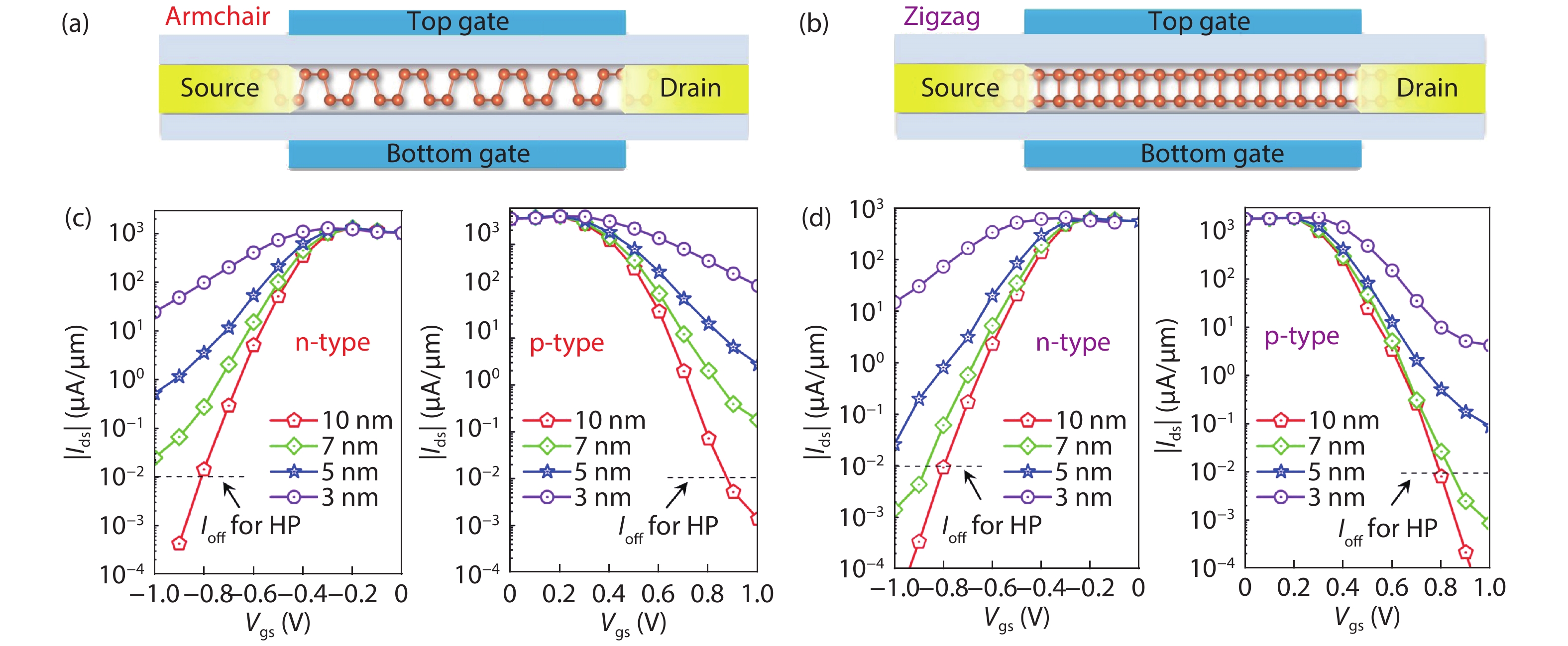
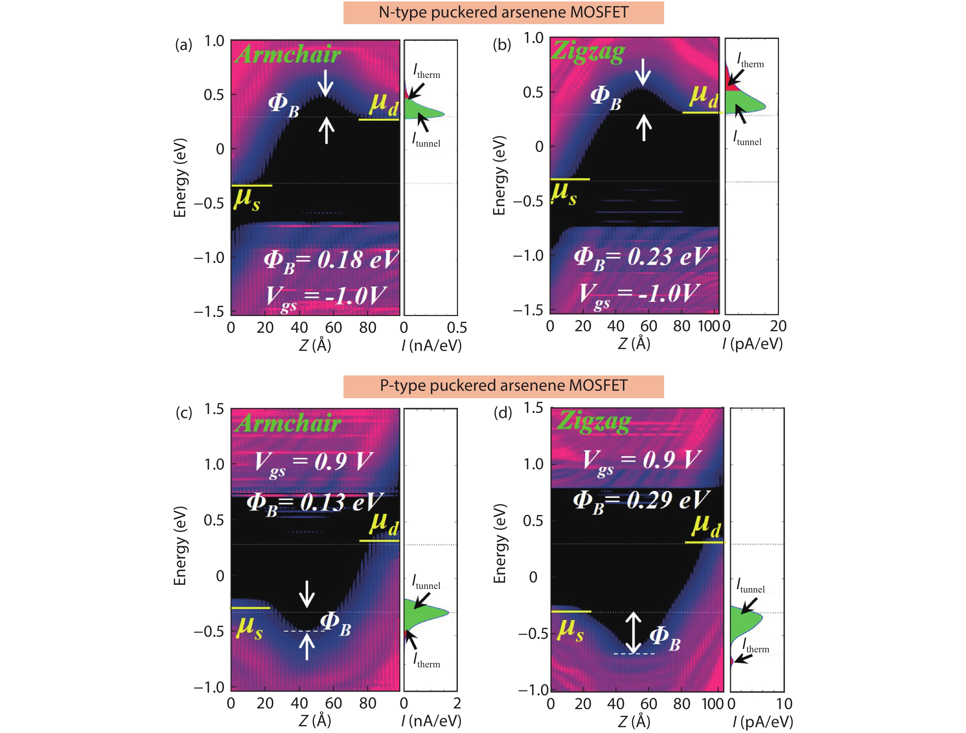
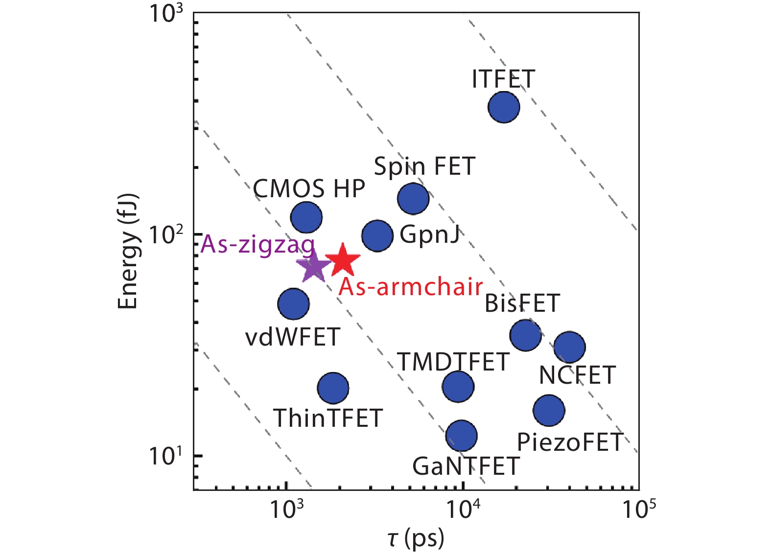
| [1] |
Chau R, Doyle B, Datta S, et al. Integrated nanoelectronics for the future. Nat Mater, 2007, 6, 810 doi: 10.1038/nmat2014 |
| [2] |
Franklin A D. Nanomaterials in transistors: From high-performance to thin-film applications. Science, 2015, 349, aab2750 doi: 10.1126/science.aab2750 |
| [3] |
Desai S B, Madhvapathy S R, Sachid A B, et al. MoS 2 transistors with 1-nanometer gate lengths. Science, 2016, 354, 99 doi: 10.1126/science.aah4698 |
| [4] |
Zhang S L, Guo S Y, Chen Z F, et al. Recent progress in 2D group-VA semiconductors: From theory to experiment. Chem Soc Rev, 2018, 47, 982 doi: 10.1039/C7CS00125H |
| [5] |
Guo S Y, Zhang Y P, Ge Y Q, et al. 2D V-V binary materials: Status and challenges. Adv Mater, 2019, 31, 1902352 doi: 10.1002/adma.201902352 |
| [6] |
Zhou W H, Zhang S L, Guo S Y, et al. Designing sub-10-nm metal-oxide-semiconductor field-effect transistors via ballistic transport and disparate effective mass: The case of two-dimensional BiN. Phys Rev Appl, 2020, 13, 044066 doi: 10.1103/PhysRevApplied.13.044066 |
| [7] |
Cao W, Kang J H, Sarkar D, et al. 2D semiconductor FETs: Projections and design for sub-10 nm VLSI. IEEE Trans Electron Devices, 2015, 62, 3459 doi: 10.1109/TED.2015.2443039 |
| [8] |
Zhu Z L, Cai X L, Yi S, et al. Multivalency-driven formation of Te-based monolayer materials: A combined first-principles and experimental study. Phys Rev Lett, 2017, 119, 106101 doi: 10.1103/PhysRevLett.119.106101 |
| [9] |
Zhou Z Q, Cui Y, Tan P H, et al. Optical and electrical properties of two-dimensional anisotropic materials. J Semicond, 2019, 40, 061001 doi: 10.1088/1674-4926/40/6/061001 |
| [10] |
Zhou W H, Chen J Y, Bai P X, et al. Two-dimensional pnictogen for field-effect transistors. Res Wash D C, 2019, 2019, 1046329 doi: 10.34133/2019/1046329 |
| [11] |
Novoselov K S, Mishchenko A, Carvalho A, et al. 2D materials and van der Waals heterostructures. Science, 2016, 353, aac9439 doi: 10.1126/science.aac9439 |
| [12] |
Wang S X, Yu Z H, Wang X R. Electrical contacts to two-dimensional transition-metal dichalcogenides. J Semicond, 2018, 39, 124001 doi: 10.1088/1674-4926/39/12/124001 |
| [13] |
|
| [14] |
Tao L, Cinquanta E, Chiappe D, et al. Silicene field-effect transistors operating at room temperature. Nat Nanotechnol, 2015, 10, 227 doi: 10.1038/nnano.2014.325 |
| [15] |
Nourbakhsh A, Zubair A, Sajjad R N, et al. MoS 2 field-effect transistor with sub-10 nm channel length. Nano Lett, 2016, 16, 7798 doi: 10.1021/acs.nanolett.6b03999 |
| [16] |
Qiao J S, Kong X H, Hu Z X, et al. High-mobility transport anisotropy and linear dichroism in few-layer black phosphorus. Nat Commun, 2014, 5, 4475 doi: 10.1038/ncomms5475 |
| [17] |
Zhang S L, Yan Z, Li Y F, et al. Atomically thin arsenene and antimonene: Semimetal –semiconductor and indirect-direct band-gap transitions. Angew Chem Int Ed, 2015, 54, 3112 doi: 10.1002/anie.201411246 |
| [18] |
Li L K, Yu Y J, Ye G J, et al. Black phosphorus field-effect transistors. Nat Nanotechnol, 2014, 9, 372 doi: 10.1038/nnano.2014.35 |
| [19] |
Wang X X, Hu Y, Mo J B, et al. Arsenene: A potential therapeutic agent for acute promyelocytic leukaemia cells by acting on nuclear proteins. Angew Chem Int Ed, 2020, 59, 5151 doi: 10.1002/anie.201913675 |
| [20] |
Zhong M Z, Xia Q L, Pan L F, et al. Thickness-dependent carrier transport characteristics of a new 2D elemental semiconductor: Black arsenic. Adv Funct Mater, 2018, 28, 1802581 doi: 10.1002/adfm.201802581 |
| [21] |
Wu X, Shao Y, Liu H, et al. Epitaxial growth and air-stability of monolayer antimonene on PdTe 2. Adv Mater, 2017, 29, 1605407 doi: 10.1002/adma.201605407 |
| [22] |
Chen Y B, Chen C Y, Kealhofer R, et al. Black arsenic: A layered semiconductor with extreme in-plane anisotropy. Adv Mater, 2018, 30, 1800754 doi: 10.1002/adma.201800754 |
| [23] |
Pizzi G, Gibertini M, Dib E, et al. Performance of arsenene and antimonene double-gate MOSFETs from first principles. Nat Commun, 2016, 7, 12585 doi: 10.1038/ncomms12585 |
| [24] |
Quhe R G, Li Q H, Zhang Q X, et al. Simulations of quantum transport in sub-5-nm monolayer phosphorene transistors. Phys Rev Appl, 2018, 10, 024022 doi: 10.1103/PhysRevApplied.10.024022 |
| [25] |
Wang J, Cai Q, Lei J M, et al. Performance of monolayer blue phosphorene double-gate MOSFETs from the first principles. ACS Appl Mater Interfaces, 2019, 11, 20956 doi: 10.1021/acsami.9b02192 |
| [26] |
Wang Y Y, Huang P, Ye M, et al. Many-body effect, carrier mobility, and device performance of hexagonal arsenene and antimonene. Chem Mater, 2017, 29, 2191 doi: 10.1021/acs.chemmater.6b04909 |
| [27] |
Kresse G, Furthmüller J. Efficient iterative schemes forab initiototal-energy calculations using a plane-wave basis set. Phys Rev B, 1996, 54, 11169 doi: 10.1103/PhysRevB.54.11169 |
| [28] |
Perdew J P, Burke K, Ernzerhof M. Generalized gradient approximation made simple. Phys Rev Lett, 1996, 77, 3865 doi: 10.1103/PhysRevLett.77.3865 |
| [29] |
Grimme S, Ehrlich S, Goerigk L. Effect of the damping function in dispersion corrected density functional theory. J Comput Chem, 2011, 32, 1456 doi: 10.1002/jcc.21759 |
| [30] |
Takagi S, Toriumi A, Iwase M, et al. On the universality of inversion layer mobility in Si MOSFET's: Part II-effects of surface orientation. IEEE Trans Electron Devices, 1994, 41, 2363 doi: 10.1109/16.337450 |
| [31] |
Atomistix Toolkit vertion 2019.03, Synopsys QuantumWise A/S
|
| [32] |
Datta S. Quantum transport: atom to transistor. Cambridge: Cambridge University Press, 2005
|
| [33] |
Gaddemane G, Vandenberghe W G, van de Put M L, et al. Theoretical studies of electronic transport in monolayer and bilayer phosphorene: A critical overview. Phys Rev B, 2018, 98, 115416 doi: 10.1103/PhysRevB.98.115416 |
| [34] |
Poncé S, Margine E R, Giustino F. Towards predictive many-body calculations of phonon-limited carrier mobilities in semiconductors. Phys Rev B, 2018, 97, 121201 doi: 10.1103/PhysRevB.97.121201 |
| [35] |
|
| [36] |
Nikonov D E, Young I A. Overview of beyond-CMOS devices and a uniform methodology for their benchmarking. Proc IEEE, 2013, 101, 2498 doi: 10.1109/JPROC.2013.2252317 |
| [37] |
Nikonov D E, Young I A. Benchmarking of beyond-CMOS exploratory devices for logic integrated circuits. IEEE J Explor Solid-State Comput Devices Circuits, 2015, 1, 3 doi: 10.1109/JXCDC.2015.2418033 |


 DownLoad: