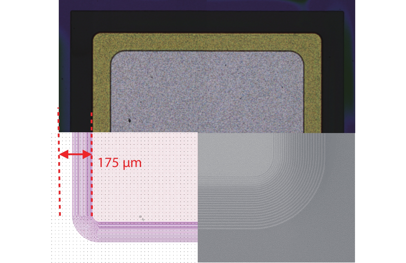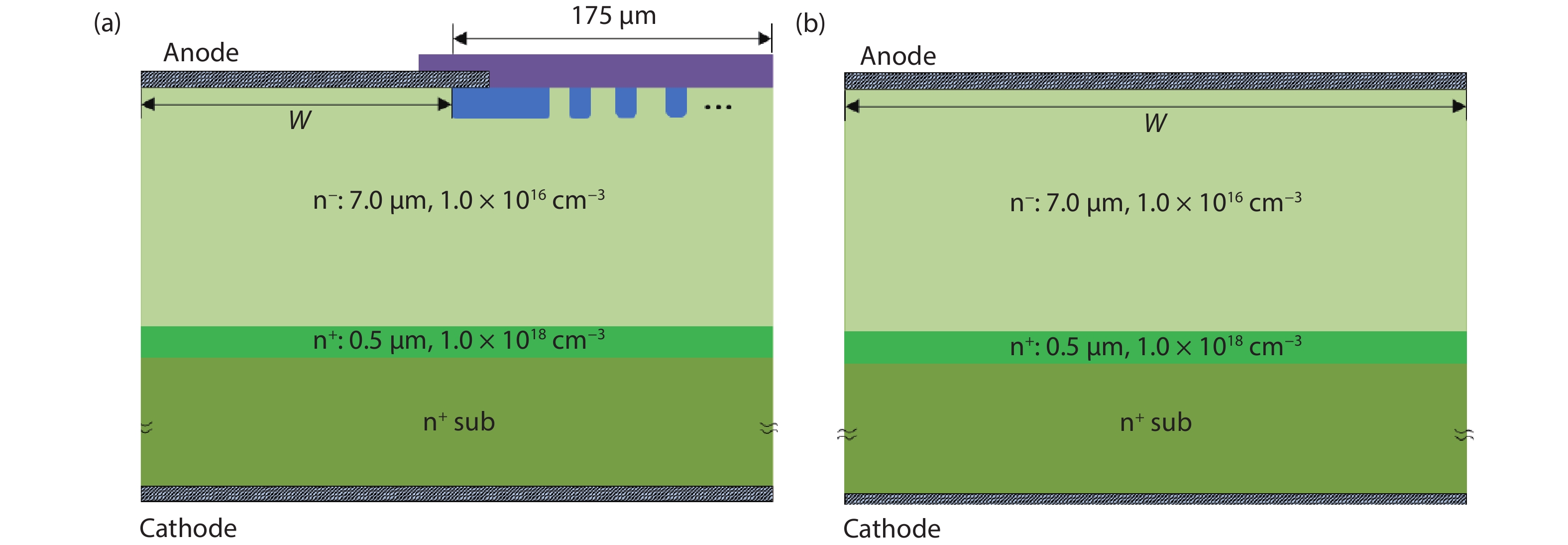
Fig. 1.
(Color online) Schematics of the device structures used in the simulation. (a) Considering the lateral spreading current. (b) Ignoring the lateral spreading current.
ARTICLES
Xi Wang1, 2, Yiwen Zhong1, Hongbin Pu1, 2, , Jichao Hu1, 2, Xianfeng Feng1, 2 and Guowen Yang3
Corresponding author: Hongbin Pu, puhongbin@xaut.edu.cn
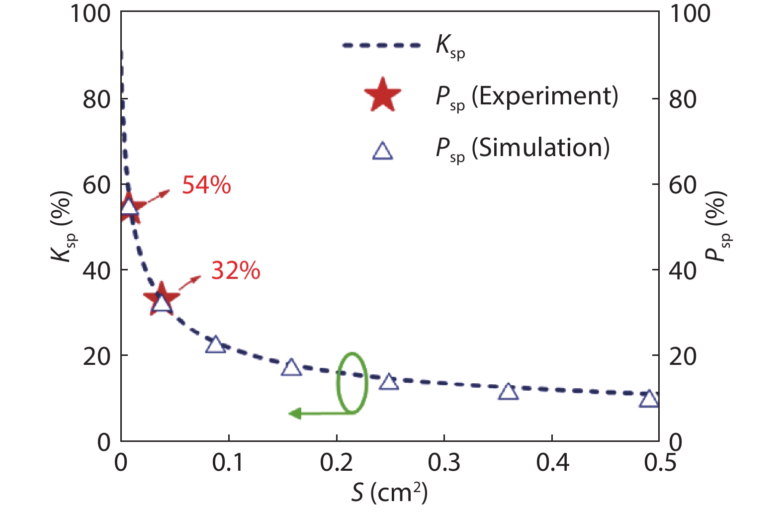
Abstract: Lateral current spreading in the 4H-SiC Schottky barrier diode (SBD) chip is investigated. The 4H-SiC SBD chips with the same vertical parameters are simulated and fabricated. The results indicate that there is a fixed spreading resistance at on-state in current spreading region for a specific chip. The linear specific spreading resistance at the on-state is calculated to be 8.6 Ω/cm in the fabricated chips. The proportion of the lateral spreading current in total forward current (Psp) is related to anode voltage and the chip area. Psp is increased with the increase in the anode voltage during initial on-state and then tends to a stable value. The stable values of Psp of the two fabricated chips are 32% and 54%. Combined with theoretical analysis, the proportion of the terminal region and scribing trench in a whole chip (Ksp) is also calculated and compared with Psp. The Ksp values of the two fabricated chips are calculated to be 31.94% and 57.75%. The values of Ksp and Psp are close with each other in a specific chip. The calculated Ksp can be used to predict that when the chip area of SiC SBD becomes larger than 0.5 cm2, the value of Psp would be lower than 10%.
Key words: 4H-SiC, Schottky barrier diode, lateral spreading current
| [1] |
Kimoto T, Yonezawa Y. Current status and perspectives of ultrahigh-voltage SiC power devices. Mater Sci Semicond Process, 2018, 78, 43 doi: 10.1016/j.mssp.2017.10.010
|
| [2] |
Yuan X B, Laird I, Walder S. Opportunities, challenges, and potential solutions in the application of fast-switching SiC power devices and converters. IEEE Trans Power Electron, 2021, 36, 3925 doi: 10.1109/TPEL.2020.3024862
|
| [3] |
Liu H Z, Wang J, Liang S W, et al. Physical modeling and design optimization of 4H-SiC insulated gate bipolar transistors for dv/dt reduction. Semicond Sci Technol, 2020, 36, 025009 doi: 10.1088/1361-6641/abcb18
|
| [4] |
Li J L, Meng C X, Yu L, et al. Effect of various defects on 4H-SiC Schottky diode performance and its relation to epitaxial growth conditions. Micromachines, 2020, 11, 609 doi: 10.3390/mi11060609
|
| [5] |
Ivanov P A, Potapov A S, Lebedeva N M, et al. Avalanche breakdown in 4H-SiC Schottky diodes: Reliability aspects. Tech Phys, 2020, 65, 2041 doi: 10.1134/S1063784220120117
|
| [6] |
Wang X, Pu H B, Liu Q, et al. Demonstration of 4H-SiC thyristor triggered by 100-mW/cm2 UV light. IEEE Electron Device Lett, 2020, 41, 824 doi: 10.1109/LED.2020.2988913
|
| [7] |
Rupp R, Treu M, Mauder A, et al. Performance and reliability issues of SiC-Schottky diodes. Mater Sci Forum, 2000, 338–342, 1167 doi: 10.4028/www.scientific.net/MSF.338-342.1167
|
| [8] |
Yuan X B, Walder S, Oswald N. EMI generation characteristics of SiC and Si diodes: Influence of reverse-recovery characteristics. IEEE Trans Power Electron, 2015, 30, 1131 doi: 10.1109/TPEL.2014.2340404
|
| [9] |
Liu L, Wu J P, Ren N, et al. 1200-V 4H-SiC merged p-i-n Schottky diodes with high avalanche capability. IEEE Trans Electron Devices, 2020, 67, 3679 doi: 10.1109/TED.2020.3007136
|
| [10] |
Zaťko B, Hrubčín L, Šagátová A, et al. Study of Schottky barrier detectors based on a high quality 4H-SiC epitaxial layer with different thickness. Appl Surf Sci, 2021, 536, 147801 doi: 10.1016/j.apsusc.2020.147801
|
| [11] |
Raja P V, Narasimha Murty N V L. Thermally annealed gamma irradiated Ni/4H-SiC Schottky barrier diode characteristics. J Semicond, 2019, 40, 022804 doi: 10.1088/1674-4926/40/2/022804
|
| [12] |
Yuan H, Liu Y C, He Y J, et al. Characteristic and robustness of trench floating limiting rings for 4H-SiC junction barrier Schottky rectifiers. IEEE Electron Device Lett, 2020, 41, 1056 doi: 10.1109/LED.2020.2993590
|
| [13] |
Elpelt R, Draghici M, Gerlach R, et al. SiC MPS devices: One step closer to the ideal diode. Mater Sci Forum, 2018, 924, 609 doi: 10.4028/www.scientific.net/MSF.924.609
|
| [14] |
Palanisamy S, Kowalsky J, Lutz J, et al. Repetitive surge current test of SiC MPS diode with load in bipolar regime. 2018 IEEE 30th International Symposium on Power Semiconductor Devices and ICs (ISPSD), 2018, 367 doi: 10.1109/ISPSD.2018.8393679
|
| [15] |
Song Q W, Yuan H, Sun Q J, et al. Reverse-bias stress-induced electrical parameters instability in 4H-SiC JBS diodes terminated nonequidistance FLRs. IEEE Trans Electron Devices, 2019, 66, 3935 doi: 10.1109/TED.2019.2931737
|
| [16] |
Zhang Q, Sudarshan T S. Lateral current spreading in SiC Schottky diodes using metal overlap edge termination. Solid State Electron, 2001, 45, 1847 doi: 10.1016/S0038-1101(01)00191-5
|
| [17] |
Kimoto T, Cooper J A. Fundamentals of silicon carbide technology. Singapore: John Wiley & Sons Singapore Pte. Ltd, 2014
|
| [18] |
Ivanov I G, Henry A, Janzén E. Ionization energies of phosphorus and nitrogen donors and aluminum acceptors in 4H silicon carbide from the donor-acceptor pair emission. Phys Rev B, 2005, 71, 241201 doi: 10.1103/PhysRevB.71.241201
|
| [19] |
Stefanakis D, Zekentes K. TCAD models of the temperature and doping dependence of the bandgap and low field carrier mobility in 4H-SiC. Microelectron Eng, 2014, 116, 65 doi: 10.1016/j.mee.2013.10.002
|
| [20] |
Zhao Y, Niwa H, Kimoto T. Impact ionization coefficients of 4H-SiC in a wide temperature range. Jpn J Appl Phys, 2019, 58, 018001 doi: 10.7567/1347-4065/aae985
|
| [21] |
Hao Y. The study on the design and experiment of advanced 4H-SiC SBD/JBS. Xidian University Press, 2017
|
| [22] |
Zhu L, Chow T P. Analytical modeling of high-voltage 4H-SiC junction barrier Schottky (JBS) rectifiers. IEEE Trans Electron Devices, 2008, 55, 1857 doi: 10.1109/TED.2008.926638
|
| [23] |
Ren N, Sheng K. An analytical model with 2-D effects for 4H-SiC trenched junction barrier Schottky diodes. IEEE Trans Electron Devices, 2014, 61, 4158 doi: 10.1109/TED.2014.2365519
|
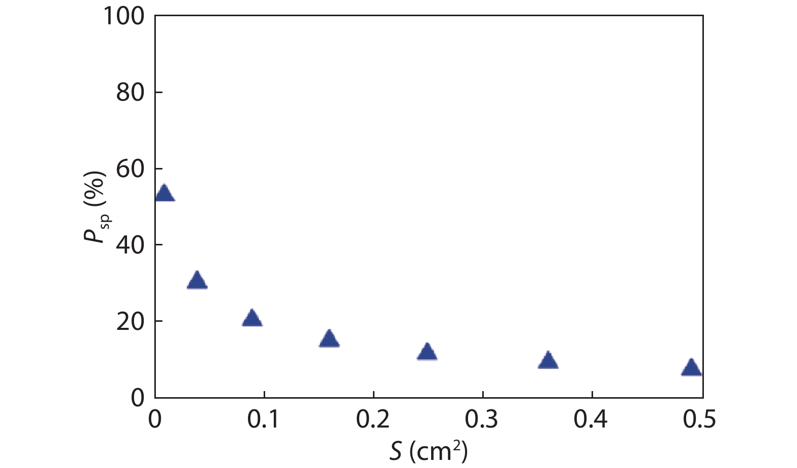
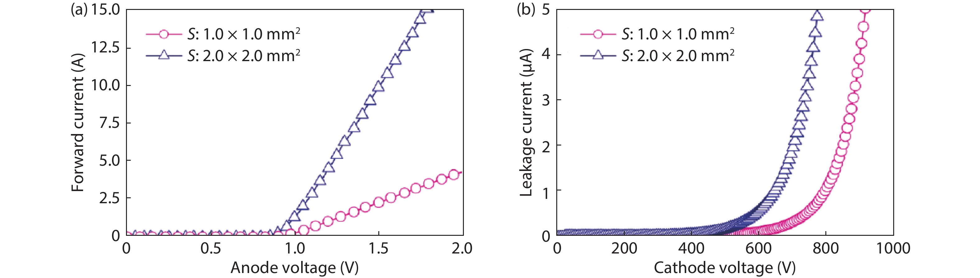
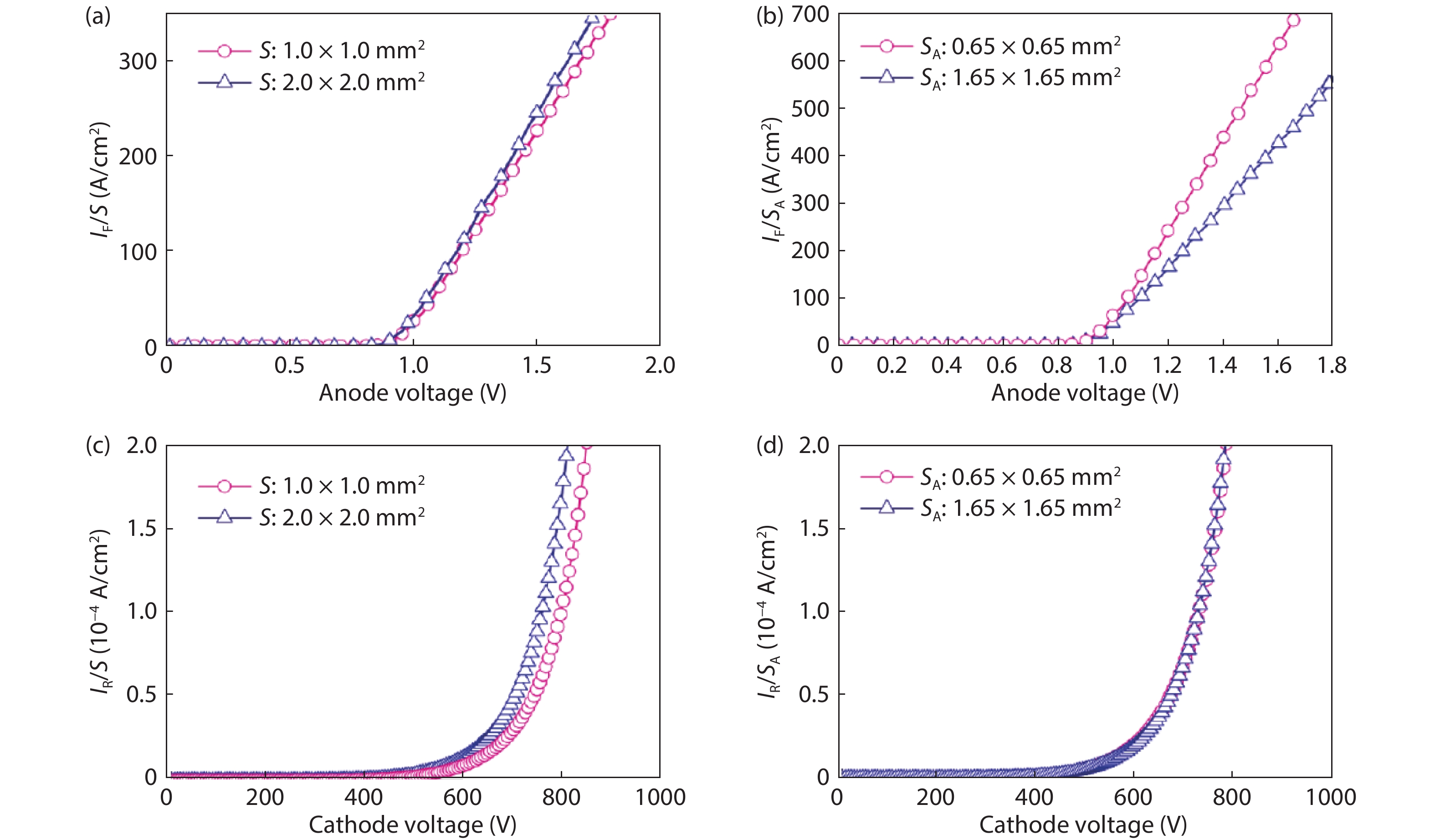
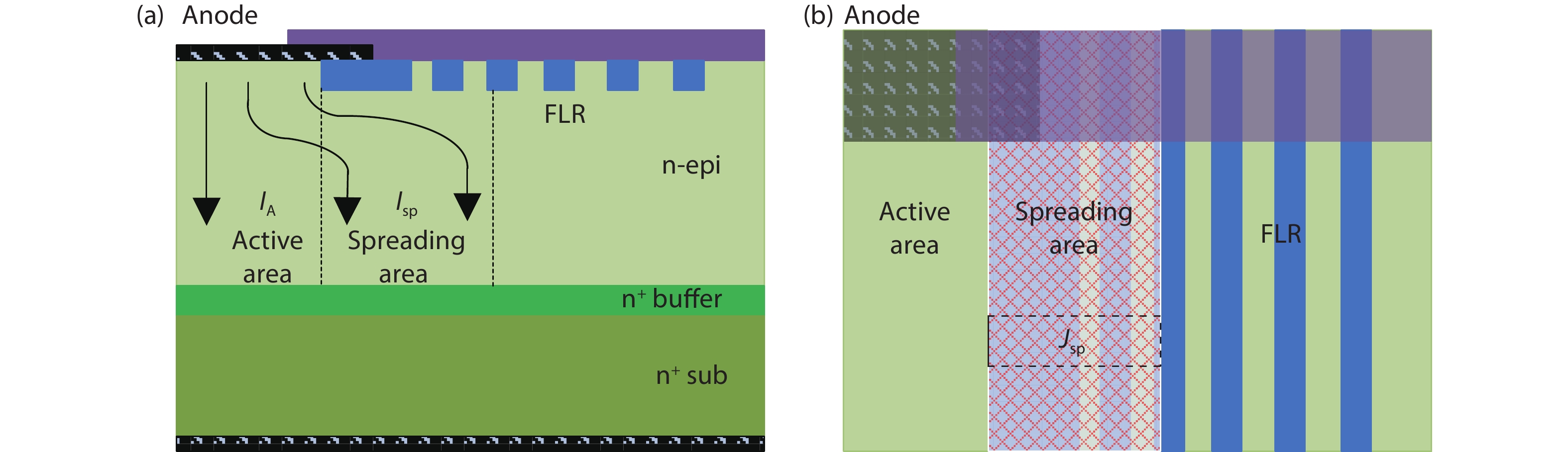
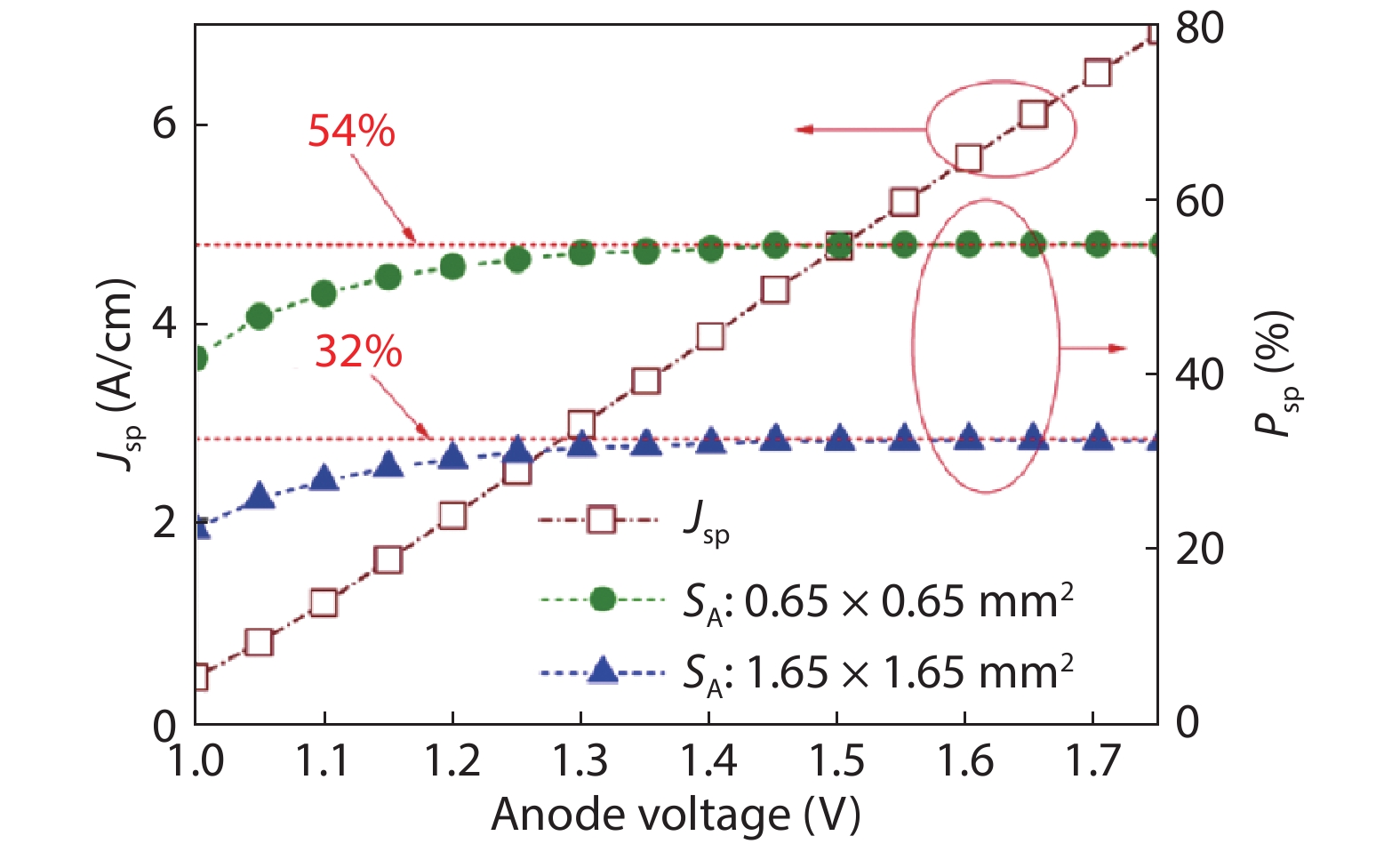
Table 1. Models and parameters used in the simulation.
| Model | Parameter |
| Bandgap energy model[17] | |
| Incomplete ionization model[18] | |
| Mobility model[19] | |
| Impact ionization model[20] | |
| Schottky contact model[21] |
 DownLoad: CSV
| [1] |
Kimoto T, Yonezawa Y. Current status and perspectives of ultrahigh-voltage SiC power devices. Mater Sci Semicond Process, 2018, 78, 43 doi: 10.1016/j.mssp.2017.10.010
|
| [2] |
Yuan X B, Laird I, Walder S. Opportunities, challenges, and potential solutions in the application of fast-switching SiC power devices and converters. IEEE Trans Power Electron, 2021, 36, 3925 doi: 10.1109/TPEL.2020.3024862
|
| [3] |
Liu H Z, Wang J, Liang S W, et al. Physical modeling and design optimization of 4H-SiC insulated gate bipolar transistors for dv/dt reduction. Semicond Sci Technol, 2020, 36, 025009 doi: 10.1088/1361-6641/abcb18
|
| [4] |
Li J L, Meng C X, Yu L, et al. Effect of various defects on 4H-SiC Schottky diode performance and its relation to epitaxial growth conditions. Micromachines, 2020, 11, 609 doi: 10.3390/mi11060609
|
| [5] |
Ivanov P A, Potapov A S, Lebedeva N M, et al. Avalanche breakdown in 4H-SiC Schottky diodes: Reliability aspects. Tech Phys, 2020, 65, 2041 doi: 10.1134/S1063784220120117
|
| [6] |
Wang X, Pu H B, Liu Q, et al. Demonstration of 4H-SiC thyristor triggered by 100-mW/cm2 UV light. IEEE Electron Device Lett, 2020, 41, 824 doi: 10.1109/LED.2020.2988913
|
| [7] |
Rupp R, Treu M, Mauder A, et al. Performance and reliability issues of SiC-Schottky diodes. Mater Sci Forum, 2000, 338–342, 1167 doi: 10.4028/www.scientific.net/MSF.338-342.1167
|
| [8] |
Yuan X B, Walder S, Oswald N. EMI generation characteristics of SiC and Si diodes: Influence of reverse-recovery characteristics. IEEE Trans Power Electron, 2015, 30, 1131 doi: 10.1109/TPEL.2014.2340404
|
| [9] |
Liu L, Wu J P, Ren N, et al. 1200-V 4H-SiC merged p-i-n Schottky diodes with high avalanche capability. IEEE Trans Electron Devices, 2020, 67, 3679 doi: 10.1109/TED.2020.3007136
|
| [10] |
Zaťko B, Hrubčín L, Šagátová A, et al. Study of Schottky barrier detectors based on a high quality 4H-SiC epitaxial layer with different thickness. Appl Surf Sci, 2021, 536, 147801 doi: 10.1016/j.apsusc.2020.147801
|
| [11] |
Raja P V, Narasimha Murty N V L. Thermally annealed gamma irradiated Ni/4H-SiC Schottky barrier diode characteristics. J Semicond, 2019, 40, 022804 doi: 10.1088/1674-4926/40/2/022804
|
| [12] |
Yuan H, Liu Y C, He Y J, et al. Characteristic and robustness of trench floating limiting rings for 4H-SiC junction barrier Schottky rectifiers. IEEE Electron Device Lett, 2020, 41, 1056 doi: 10.1109/LED.2020.2993590
|
| [13] |
Elpelt R, Draghici M, Gerlach R, et al. SiC MPS devices: One step closer to the ideal diode. Mater Sci Forum, 2018, 924, 609 doi: 10.4028/www.scientific.net/MSF.924.609
|
| [14] |
Palanisamy S, Kowalsky J, Lutz J, et al. Repetitive surge current test of SiC MPS diode with load in bipolar regime. 2018 IEEE 30th International Symposium on Power Semiconductor Devices and ICs (ISPSD), 2018, 367 doi: 10.1109/ISPSD.2018.8393679
|
| [15] |
Song Q W, Yuan H, Sun Q J, et al. Reverse-bias stress-induced electrical parameters instability in 4H-SiC JBS diodes terminated nonequidistance FLRs. IEEE Trans Electron Devices, 2019, 66, 3935 doi: 10.1109/TED.2019.2931737
|
| [16] |
Zhang Q, Sudarshan T S. Lateral current spreading in SiC Schottky diodes using metal overlap edge termination. Solid State Electron, 2001, 45, 1847 doi: 10.1016/S0038-1101(01)00191-5
|
| [17] |
Kimoto T, Cooper J A. Fundamentals of silicon carbide technology. Singapore: John Wiley & Sons Singapore Pte. Ltd, 2014
|
| [18] |
Ivanov I G, Henry A, Janzén E. Ionization energies of phosphorus and nitrogen donors and aluminum acceptors in 4H silicon carbide from the donor-acceptor pair emission. Phys Rev B, 2005, 71, 241201 doi: 10.1103/PhysRevB.71.241201
|
| [19] |
Stefanakis D, Zekentes K. TCAD models of the temperature and doping dependence of the bandgap and low field carrier mobility in 4H-SiC. Microelectron Eng, 2014, 116, 65 doi: 10.1016/j.mee.2013.10.002
|
| [20] |
Zhao Y, Niwa H, Kimoto T. Impact ionization coefficients of 4H-SiC in a wide temperature range. Jpn J Appl Phys, 2019, 58, 018001 doi: 10.7567/1347-4065/aae985
|
| [21] |
Hao Y. The study on the design and experiment of advanced 4H-SiC SBD/JBS. Xidian University Press, 2017
|
| [22] |
Zhu L, Chow T P. Analytical modeling of high-voltage 4H-SiC junction barrier Schottky (JBS) rectifiers. IEEE Trans Electron Devices, 2008, 55, 1857 doi: 10.1109/TED.2008.926638
|
| [23] |
Ren N, Sheng K. An analytical model with 2-D effects for 4H-SiC trenched junction barrier Schottky diodes. IEEE Trans Electron Devices, 2014, 61, 4158 doi: 10.1109/TED.2014.2365519
|


Article views: 1900 Times PDF downloads: 170 Times Cited by: 0 Times
Received: 22 March 2021 Revised: 12 August 2021 Online: Accepted Manuscript: 09 October 2021Uncorrected proof: 11 October 2021Published: 01 November 2021
| Citation: |
Xi Wang, Yiwen Zhong, Hongbin Pu, Jichao Hu, Xianfeng Feng, Guowen Yang. Investigation of lateral spreading current in the 4H-SiC Schottky barrier diode chip[J]. Journal of Semiconductors, 2021, 42(11): 112802. doi: 10.1088/1674-4926/42/11/112802
X Wang, Y W Zhong, H B Pu, J C Hu, X F Feng, G W Yang, Investigation of lateral spreading current in the 4H-SiC Schottky barrier diode chip[J]. J. Semicond., 2021, 42(11): 112802. doi: 10.1088/1674-4926/42/11/112802.
Export: BibTex EndNote

|
| [1] |
Kimoto T, Yonezawa Y. Current status and perspectives of ultrahigh-voltage SiC power devices. Mater Sci Semicond Process, 2018, 78, 43 doi: 10.1016/j.mssp.2017.10.010
|
| [2] |
Yuan X B, Laird I, Walder S. Opportunities, challenges, and potential solutions in the application of fast-switching SiC power devices and converters. IEEE Trans Power Electron, 2021, 36, 3925 doi: 10.1109/TPEL.2020.3024862
|
| [3] |
Liu H Z, Wang J, Liang S W, et al. Physical modeling and design optimization of 4H-SiC insulated gate bipolar transistors for dv/dt reduction. Semicond Sci Technol, 2020, 36, 025009 doi: 10.1088/1361-6641/abcb18
|
| [4] |
Li J L, Meng C X, Yu L, et al. Effect of various defects on 4H-SiC Schottky diode performance and its relation to epitaxial growth conditions. Micromachines, 2020, 11, 609 doi: 10.3390/mi11060609
|
| [5] |
Ivanov P A, Potapov A S, Lebedeva N M, et al. Avalanche breakdown in 4H-SiC Schottky diodes: Reliability aspects. Tech Phys, 2020, 65, 2041 doi: 10.1134/S1063784220120117
|
| [6] |
Wang X, Pu H B, Liu Q, et al. Demonstration of 4H-SiC thyristor triggered by 100-mW/cm2 UV light. IEEE Electron Device Lett, 2020, 41, 824 doi: 10.1109/LED.2020.2988913
|
| [7] |
Rupp R, Treu M, Mauder A, et al. Performance and reliability issues of SiC-Schottky diodes. Mater Sci Forum, 2000, 338–342, 1167 doi: 10.4028/www.scientific.net/MSF.338-342.1167
|
| [8] |
Yuan X B, Walder S, Oswald N. EMI generation characteristics of SiC and Si diodes: Influence of reverse-recovery characteristics. IEEE Trans Power Electron, 2015, 30, 1131 doi: 10.1109/TPEL.2014.2340404
|
| [9] |
Liu L, Wu J P, Ren N, et al. 1200-V 4H-SiC merged p-i-n Schottky diodes with high avalanche capability. IEEE Trans Electron Devices, 2020, 67, 3679 doi: 10.1109/TED.2020.3007136
|
| [10] |
Zaťko B, Hrubčín L, Šagátová A, et al. Study of Schottky barrier detectors based on a high quality 4H-SiC epitaxial layer with different thickness. Appl Surf Sci, 2021, 536, 147801 doi: 10.1016/j.apsusc.2020.147801
|
| [11] |
Raja P V, Narasimha Murty N V L. Thermally annealed gamma irradiated Ni/4H-SiC Schottky barrier diode characteristics. J Semicond, 2019, 40, 022804 doi: 10.1088/1674-4926/40/2/022804
|
| [12] |
Yuan H, Liu Y C, He Y J, et al. Characteristic and robustness of trench floating limiting rings for 4H-SiC junction barrier Schottky rectifiers. IEEE Electron Device Lett, 2020, 41, 1056 doi: 10.1109/LED.2020.2993590
|
| [13] |
Elpelt R, Draghici M, Gerlach R, et al. SiC MPS devices: One step closer to the ideal diode. Mater Sci Forum, 2018, 924, 609 doi: 10.4028/www.scientific.net/MSF.924.609
|
| [14] |
Palanisamy S, Kowalsky J, Lutz J, et al. Repetitive surge current test of SiC MPS diode with load in bipolar regime. 2018 IEEE 30th International Symposium on Power Semiconductor Devices and ICs (ISPSD), 2018, 367 doi: 10.1109/ISPSD.2018.8393679
|
| [15] |
Song Q W, Yuan H, Sun Q J, et al. Reverse-bias stress-induced electrical parameters instability in 4H-SiC JBS diodes terminated nonequidistance FLRs. IEEE Trans Electron Devices, 2019, 66, 3935 doi: 10.1109/TED.2019.2931737
|
| [16] |
Zhang Q, Sudarshan T S. Lateral current spreading in SiC Schottky diodes using metal overlap edge termination. Solid State Electron, 2001, 45, 1847 doi: 10.1016/S0038-1101(01)00191-5
|
| [17] |
Kimoto T, Cooper J A. Fundamentals of silicon carbide technology. Singapore: John Wiley & Sons Singapore Pte. Ltd, 2014
|
| [18] |
Ivanov I G, Henry A, Janzén E. Ionization energies of phosphorus and nitrogen donors and aluminum acceptors in 4H silicon carbide from the donor-acceptor pair emission. Phys Rev B, 2005, 71, 241201 doi: 10.1103/PhysRevB.71.241201
|
| [19] |
Stefanakis D, Zekentes K. TCAD models of the temperature and doping dependence of the bandgap and low field carrier mobility in 4H-SiC. Microelectron Eng, 2014, 116, 65 doi: 10.1016/j.mee.2013.10.002
|
| [20] |
Zhao Y, Niwa H, Kimoto T. Impact ionization coefficients of 4H-SiC in a wide temperature range. Jpn J Appl Phys, 2019, 58, 018001 doi: 10.7567/1347-4065/aae985
|
| [21] |
Hao Y. The study on the design and experiment of advanced 4H-SiC SBD/JBS. Xidian University Press, 2017
|
| [22] |
Zhu L, Chow T P. Analytical modeling of high-voltage 4H-SiC junction barrier Schottky (JBS) rectifiers. IEEE Trans Electron Devices, 2008, 55, 1857 doi: 10.1109/TED.2008.926638
|
| [23] |
Ren N, Sheng K. An analytical model with 2-D effects for 4H-SiC trenched junction barrier Schottky diodes. IEEE Trans Electron Devices, 2014, 61, 4158 doi: 10.1109/TED.2014.2365519
|

 WeChat ID
Journal of Semiconductors © 2017 All Rights Reserved 京ICP备05085259号-2