


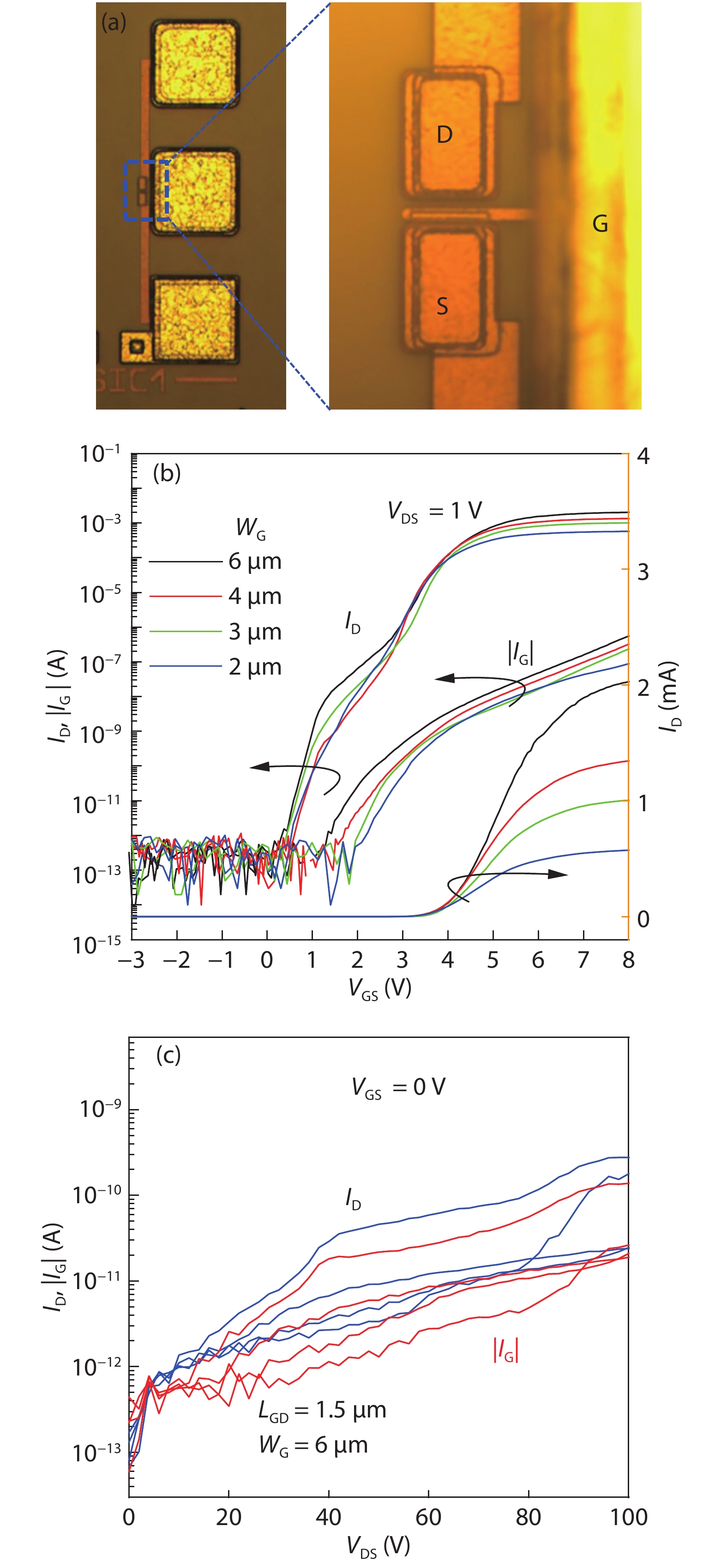
Fig. 1.
(Color online) Fabricated 200 mm GaN-on-SOI wafer with CMOS-compatible processing.
ARTICLES
Xiangdong Li1, 2, , Karen Geens1, Nooshin Amirifar1, Ming Zhao1, Shuzhen You1, Niels Posthuma1, Hu Liang1, Guido Groeseneken1, 2 and Stefaan Decoutere1
Corresponding author: Xiangdong Li, lixiangdong28@126.com
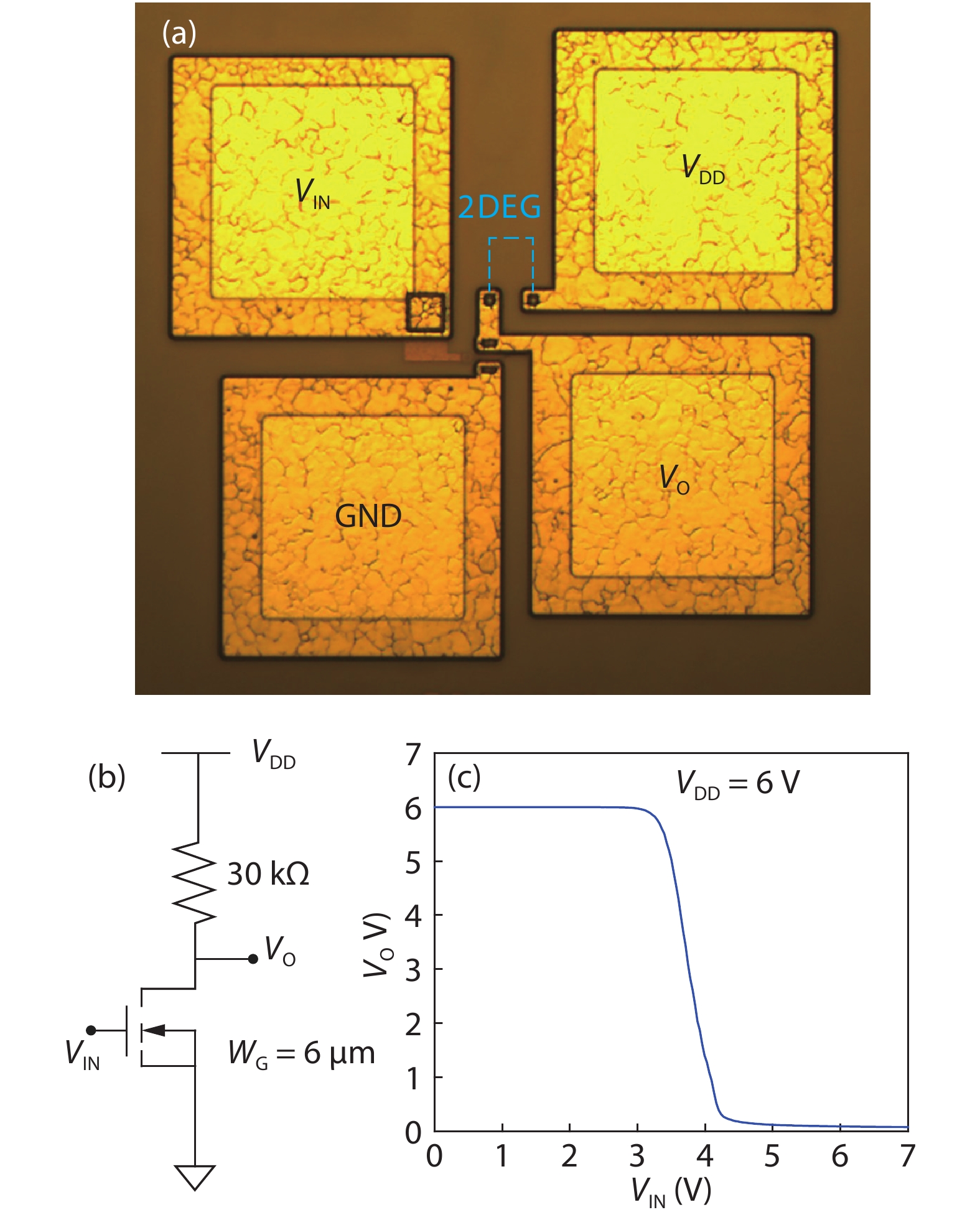
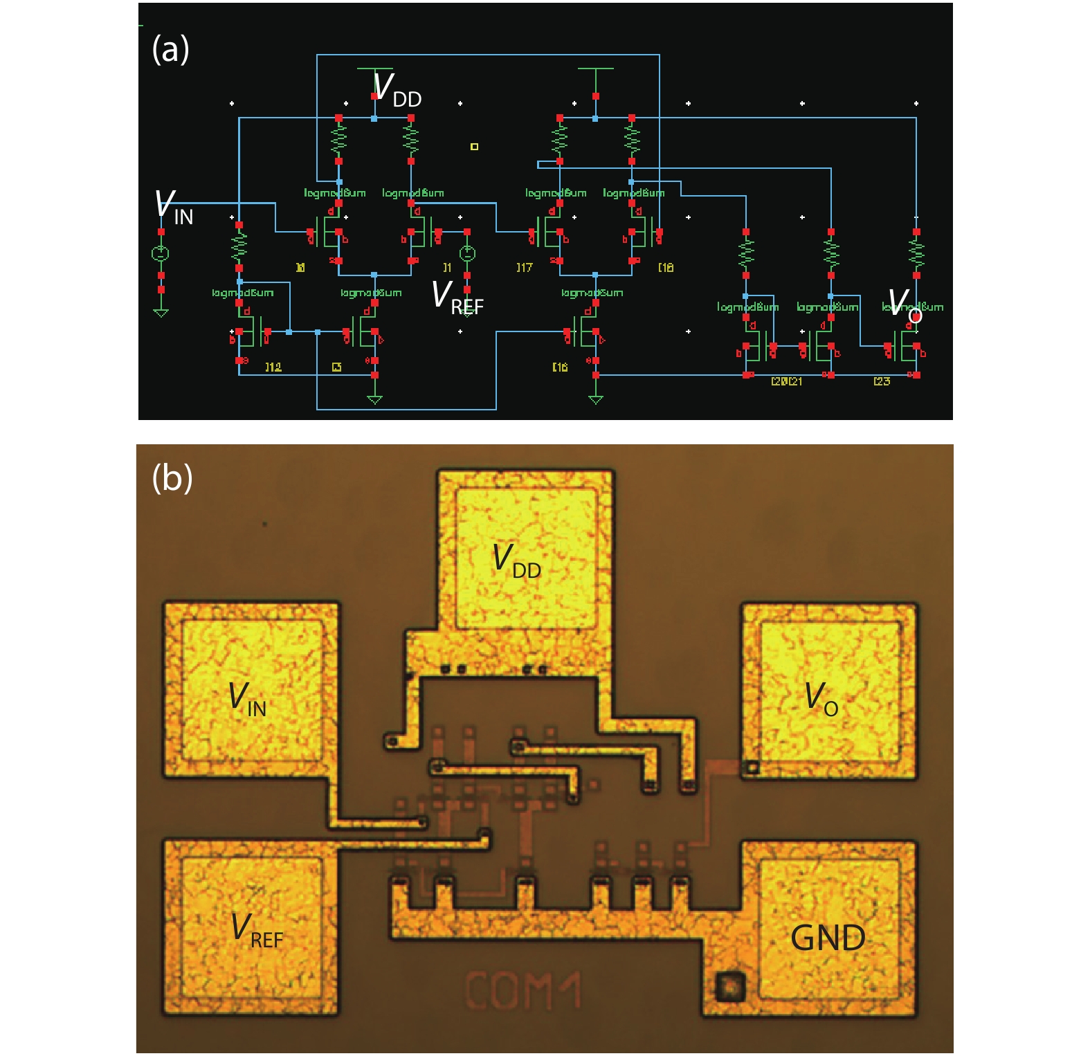
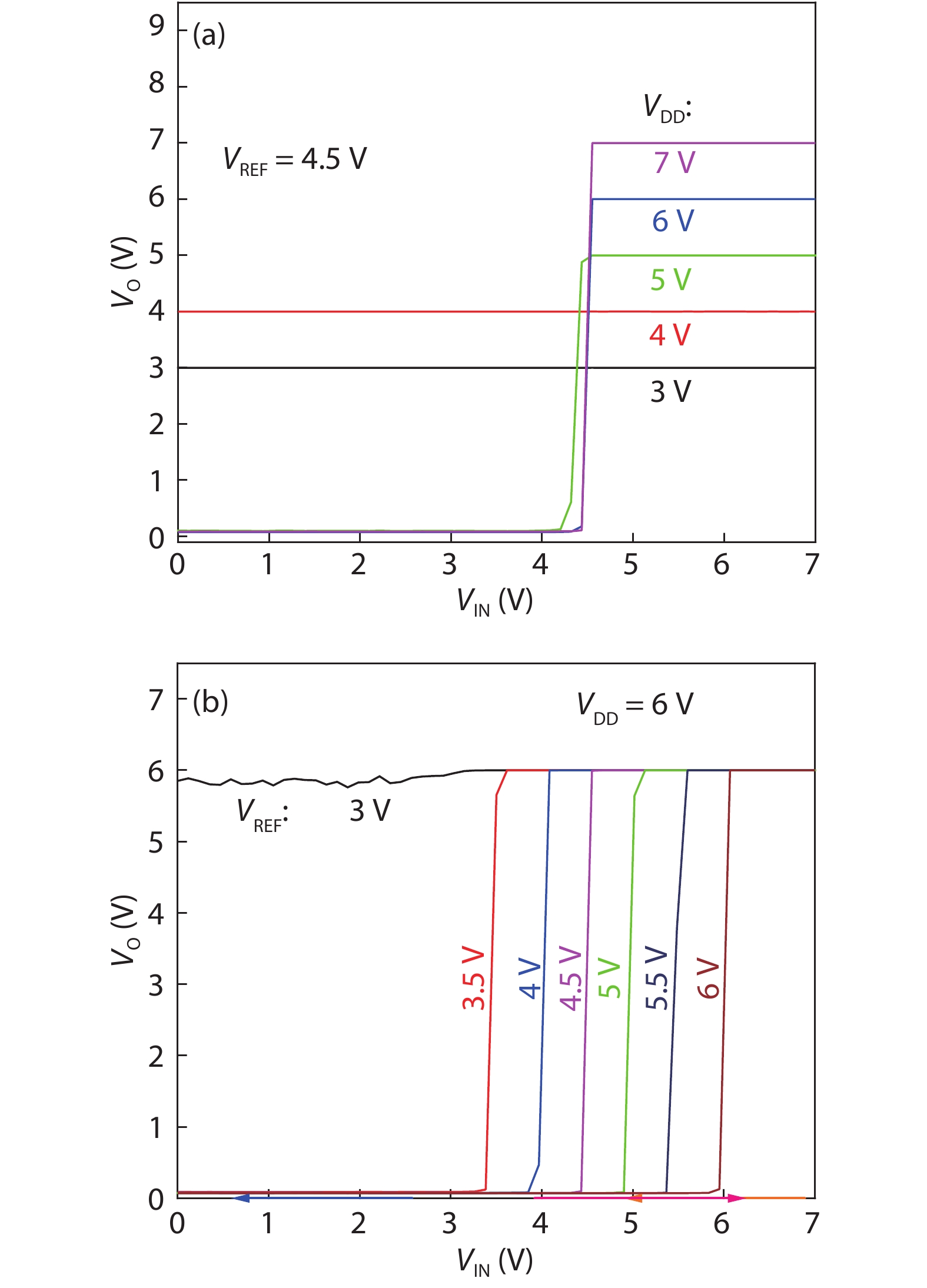
Abstract: We demonstrate the key module of comparators in GaN ICs, based on resistor-transistor logic (RTL) on E-mode wafers in this work. The fundamental inverters in the comparator consist of a p-GaN gate HEMT and a 2DEG resistor as the load. The function of the RTL comparators is finally verified by a undervoltage lockout (UVLO) circuit. The compatibility of this circuit with the current p-GaN technology paves the way for integrating logic ICs together with the power devices.
Key words: p-GaN, resistor-transistor logic (RTL), comparator, undervoltage lockout (UVLO), GaN ICs
| [1] |
Dan K. GaN power IC technology: Past, present, and future. 2017 29th International Symposium on Power Semiconductor Devices and IC's (ISPSD), 2017, 19
|
| [2] |
Uemoto Y, Morita T, Ikoshi A, et al. GaN monolithic inverter IC using normally-off gate injection transistors with planar isolation on Si substrate. 2009 IEEE International Electron Devices Meeting (IEDM), 2009, 1
|
| [3] |
Moench S, Kallfass I, Reiner R, et al. Single-input GaN gate driver based on depletion-mode logic integrated with a 600 V GaN-on-Si power transistor. 2016 IEEE 4th Work Wide Bandgap Power Devices Appl Wipda, 2016, 204
|
| [4] |
Tang G, Kwan M H, Zhang Z, et al. High-speed, high-reliability GaN power device with integrated gate driver. Proc ISPSD, 2018, 76
|
| [5] |
Li X D, van Hove M, Zhao M, et al. 200 V enhancement-mode p-GaN HEMTs fabricated on 200 mm GaN-on-SOI with trench isolation for monolithic integration. IEEE Electron Device Lett, 2017, 38, 918 doi: 10.1109/LED.2017.2703304
|
| [6] |
Li X D, van Hove M, Zhao M, et al. Suppression of the backgating effect of enhancement-mode p-GaN HEMTs on 200-mm GaN-on-SOI for monolithic integration. IEEE Electron Device Lett, 2018, 39, 999 doi: 10.1109/LED.2018.2833883
|
| [7] |
Li X D, Geens K, Guo W M, et al. Demonstration of GaN integrated half-bridge with on-chip drivers on 200-mm engineered substrates. IEEE Electron Device Lett, 2019, 40, 1499 doi: 10.1109/LED.2019.2929417
|
| [8] |
Li X, Amirifar N, Geens K, et al. GaN-on-SOI: Monolithically integrated all-GaN ICs for power conversion. 2019 IEEE International Electron Devices Meeting (IEDM), 2019, 4.4.1
|
| [9] |
Li X D, van Hove M, Zhao M, et al. Investigation on carrier transport through AlN nucleation layer from differently doped Si(111) substrates. IEEE Trans Electron Devices, 2018, 65, 1721 doi: 10.1109/TED.2018.2810886
|
| [10] |
Li X D, Zhao M, Bakeroot B, et al. Buffer vertical leakage mechanism and reliability of 200-mm GaN-on-SOI. IEEE Trans Electron Devices, 2019, 66, 553 doi: 10.1109/TED.2018.2878457
|
| [11] |
Geens K, Li X D, Zhao M, et al. 650 V p-GaN gate power HEMTs on 200 mm engineered substrates. 2019 IEEE 7th Workshop on Wide Bandgap Power Devices and Applications (WiPDA), 2019, 292
|
| [12] |
Liu X S, Chen K J. GaN single-polarity power supply bootstrapped comparator for high-temperature electronics. IEEE Electron Device Lett, 2011, 32, 27 doi: 10.1109/LED.2010.2088376
|
| [13] |
van Hove M, Boulay S, Bahl S R, et al. CMOS process-compatible high-power low-leakage AlGaN/GaN MISHEMT on silicon. IEEE Electron Device Lett, 2012, 33, 667 doi: 10.1109/LED.2012.2188016
|
| [14] |
Wu T L, Marcon D, You S Z, et al. Forward bias gate breakdown mechanism in enhancement-mode p-GaN gate AlGaN/GaN high-electron mobility transistors. IEEE Electron Device Lett, 2015, 36, 1001 doi: 10.1109/LED.2015.2465137
|
| [15] |
GaN-IC Technology, http://europractice-ic.com/mpw-prototyping/power-electronics/
|
| [16] |
Li X D, Bakeroot B, Wu Z C, et al. Observation of dynamic V TH of p-GaN gate HEMTs by fast sweeping characterization. IEEE Electron Device Lett, 2020, 41, 577 doi: 10.1109/LED.2020.2972971
|


Article views: 4617 Times PDF downloads: 167 Times Cited by: 0 Times
Received: 01 June 2020 Revised: 28 June 2020 Online: Accepted Manuscript: 22 September 2020Uncorrected proof: 24 September 2020Published: 08 February 2021
| Citation: |
Xiangdong Li, Karen Geens, Nooshin Amirifar, Ming Zhao, Shuzhen You, Niels Posthuma, Hu Liang, Guido Groeseneken, Stefaan Decoutere. Integration of GaN analog building blocks on p-GaN wafers for GaN ICs[J]. Journal of Semiconductors, 2021, 42(2): 024103. doi: 10.1088/1674-4926/42/2/024103
****
X D Li, K Geens, N Amirifar, M Zhao, S Z You, N Posthuma, H Liang, G Groeseneken, S Decoutere, Integration of GaN analog building blocks on p-GaN wafers for GaN ICs[J]. J. Semicond., 2021, 42(2): 024103. doi: 10.1088/1674-4926/42/2/024103.

|
| [1] |
Dan K. GaN power IC technology: Past, present, and future. 2017 29th International Symposium on Power Semiconductor Devices and IC's (ISPSD), 2017, 19
|
| [2] |
Uemoto Y, Morita T, Ikoshi A, et al. GaN monolithic inverter IC using normally-off gate injection transistors with planar isolation on Si substrate. 2009 IEEE International Electron Devices Meeting (IEDM), 2009, 1
|
| [3] |
Moench S, Kallfass I, Reiner R, et al. Single-input GaN gate driver based on depletion-mode logic integrated with a 600 V GaN-on-Si power transistor. 2016 IEEE 4th Work Wide Bandgap Power Devices Appl Wipda, 2016, 204
|
| [4] |
Tang G, Kwan M H, Zhang Z, et al. High-speed, high-reliability GaN power device with integrated gate driver. Proc ISPSD, 2018, 76
|
| [5] |
Li X D, van Hove M, Zhao M, et al. 200 V enhancement-mode p-GaN HEMTs fabricated on 200 mm GaN-on-SOI with trench isolation for monolithic integration. IEEE Electron Device Lett, 2017, 38, 918 doi: 10.1109/LED.2017.2703304
|
| [6] |
Li X D, van Hove M, Zhao M, et al. Suppression of the backgating effect of enhancement-mode p-GaN HEMTs on 200-mm GaN-on-SOI for monolithic integration. IEEE Electron Device Lett, 2018, 39, 999 doi: 10.1109/LED.2018.2833883
|
| [7] |
Li X D, Geens K, Guo W M, et al. Demonstration of GaN integrated half-bridge with on-chip drivers on 200-mm engineered substrates. IEEE Electron Device Lett, 2019, 40, 1499 doi: 10.1109/LED.2019.2929417
|
| [8] |
Li X, Amirifar N, Geens K, et al. GaN-on-SOI: Monolithically integrated all-GaN ICs for power conversion. 2019 IEEE International Electron Devices Meeting (IEDM), 2019, 4.4.1
|
| [9] |
Li X D, van Hove M, Zhao M, et al. Investigation on carrier transport through AlN nucleation layer from differently doped Si(111) substrates. IEEE Trans Electron Devices, 2018, 65, 1721 doi: 10.1109/TED.2018.2810886
|
| [10] |
Li X D, Zhao M, Bakeroot B, et al. Buffer vertical leakage mechanism and reliability of 200-mm GaN-on-SOI. IEEE Trans Electron Devices, 2019, 66, 553 doi: 10.1109/TED.2018.2878457
|
| [11] |
Geens K, Li X D, Zhao M, et al. 650 V p-GaN gate power HEMTs on 200 mm engineered substrates. 2019 IEEE 7th Workshop on Wide Bandgap Power Devices and Applications (WiPDA), 2019, 292
|
| [12] |
Liu X S, Chen K J. GaN single-polarity power supply bootstrapped comparator for high-temperature electronics. IEEE Electron Device Lett, 2011, 32, 27 doi: 10.1109/LED.2010.2088376
|
| [13] |
van Hove M, Boulay S, Bahl S R, et al. CMOS process-compatible high-power low-leakage AlGaN/GaN MISHEMT on silicon. IEEE Electron Device Lett, 2012, 33, 667 doi: 10.1109/LED.2012.2188016
|
| [14] |
Wu T L, Marcon D, You S Z, et al. Forward bias gate breakdown mechanism in enhancement-mode p-GaN gate AlGaN/GaN high-electron mobility transistors. IEEE Electron Device Lett, 2015, 36, 1001 doi: 10.1109/LED.2015.2465137
|
| [15] |
GaN-IC Technology, http://europractice-ic.com/mpw-prototyping/power-electronics/
|
| [16] |
Li X D, Bakeroot B, Wu Z C, et al. Observation of dynamic V TH of p-GaN gate HEMTs by fast sweeping characterization. IEEE Electron Device Lett, 2020, 41, 577 doi: 10.1109/LED.2020.2972971
|

 WeChat ID
Journal of Semiconductors © 2017 All Rights Reserved 京ICP备05085259号-2

 DownLoad:

