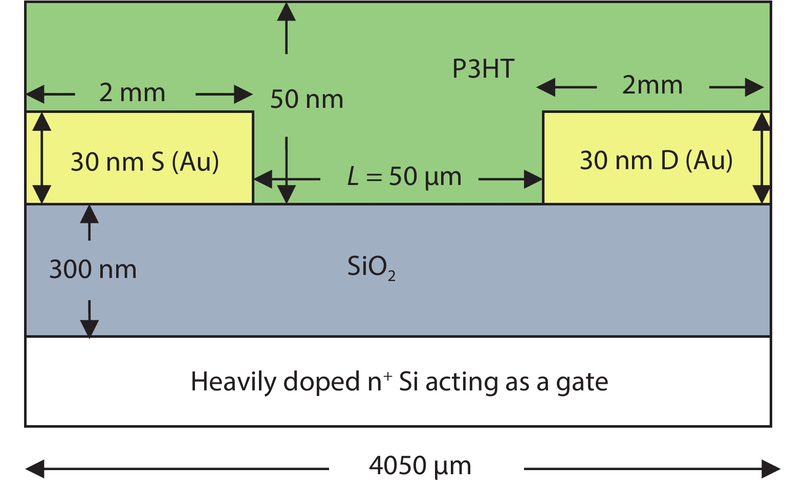
Fig. 1.
(Color online) Structure of the P3HT-based bottom-gate bottom-contact (BGBC) OTFT.
ARTICLES
Shubham Dadhich1, A. D. D. Dwivedi1, and Arun Kumar Singh2,
Corresponding author: A. D. D. Dwivedi, adddwivedi@gmail.com; Arun Kumar Singh, arunsingh.itbhu@gmail.com
Abstract: This paper presents the fabrication, characterization and numerical simulation of poly-3-hexylthiophene (P3HT)-based bottom-gate bottom-contact (BGBC) organic thin film transistors (OTFTs). The simulation is based on a drift diffusion charge transport model and density of defect states (DOS) for the traps in the band gap of the P3HT based channel. It combines two mobility models, a hopping mobility model and the Poole–Frenkel mobility model. It also describes the defect density of states (DOS) for both tail and deep states. The model takes into account all the operating regions of the OTFT and includes sub-threshold and above threshold characteristics of OTFTs. The model has been verified by comparing the numerically simulated results with the experimental results. This model is also used to simulate different structure in four configurations of OTFT e.g. bottom-gate bottom-contact (BGBC), bottom-gate top-contact (BGTC), top-gate bottom-contact (TGBC) and top-gate top-contact (TGTC) configurations of the OTFTs. We also present the compact modeling and model parameter extraction of the P3HT-based OTFTs. The extracted compact model has been further applied in a p-channel OTFT-based inverter and three stage ring oscillator circuit simulation.
| [1] |
Guo X J, Xu Y, Ogier S, et al. Current status and opportunities of organic thin-film transistor technologies. IEEE Trans Electron Devices, 2017, 64, 1906 doi: 10.1109/TED.2017.2677086
|
| [2] |
Ding L, Zhao J Q, Huang Y K, et al. Flexible-blade coating of small molecule organic semiconductor for low voltage organic field effect transistor. IEEE Electron Device Lett, 2017, 38, 338 doi: 10.1109/LED.2017.2657651
|
| [3] |
Jeong J, Kim M, Lee S H, et al. Self-defined short channel formation with micromolded separator and inkjet-printed source/drain electrodes in OTFTs. IEEE Electron Device Lett, 2011, 32, 1758 doi: 10.1109/LED.2011.2169646
|
| [4] |
Kim S H, Lee S H, Kim Y G, et al. Ink-jet-printed organic thin-film transistors for low-voltage-driven CMOS circuits with solution-processed AlOx gate insulator. IEEE Electron Device Lett, 2013, 34, 307 doi: 10.1109/LED.2012.2228461
|
| [5] |
Marien H, Steyaert M S J, van Veenendaal E, et al. Analog building blocks for organic smart sensor systems in organic thin-film transistor technology on flexible plastic foil. IEEE J Solid-State Circuits, 2012, 47, 1712 doi: 10.1109/JSSC.2012.2191038
|
| [6] |
Scarpa G, Idzko A L, Münzer A, et al. Low-cost solution-processable organic thin-film transistors for (bio)sensing applications. 2011 IEEE Sensors, 2011, 1581
|
| [7] |
Mohamad K A, Alias A, Saad I, et al. All-polymer organic field-effect transistors with memory element. 2012 Third International Conference on Intelligent Systems Modelling and Simulation, 2012, 743
|
| [8] |
Xu M L, Guo S X, Xiang L Y, et al. High mobility flexible ferroelectric organic transistor nonvolatile memory with an ultrathin AlOx interfacial layer. IEEE Trans Electron Devices, 2018, 65, 1113 doi: 10.1109/TED.2018.2797936
|
| [9] |
Wang A, Kymissis I, Bulovic V, et al. Engineering density of semiconductor-dielectric interface states to modulate threshold voltage in OFETs. IEEE Trans Electron Devices, 2006, 53, 9 doi: 10.1109/TED.2005.860633
|
| [10] |
Ramos B, Lopes M, Buso D, et al. Performance enhancement in N-channel organic field-effect transistors using ferroelectric material as a gate dielectric. IEEE Trans Nanotechnol, 2017, 16, 773 doi: 10.1109/TNANO.2017.2683201
|
| [11] |
Feng L R, Zhao J Q, Tang W, et al. Solution processed organic thin-film transistors with hybrid low/high voltage operation. J Disp Technol, 2014, 10, 971 doi: 10.1109/JDT.2014.2344040
|
| [12] |
Mizukami M, Oku S, Cho S I, et al. A solution-processed organic thin-film transistor backplane for flexible multiphoton emission organic light-emitting diode displays. IEEE Electron Device Lett, 2015, 36, 841 doi: 10.1109/LED.2015.2443184
|
| [13] |
Takshi A, Dimopoulos A, Madden J D. Simulation of a low-voltage organic transistor compatible with printing methods. IEEE Trans Electron Devices, 2008, 55, 276 doi: 10.1109/TED.2007.910615
|
| [14] |
Jiménez Tejada J A, López Varo P, Cammidge A N, et al. Compact modeling of organic thin-film transistors with solution processed octadecyl substituted tetrabenzotriazaporphyrin as an active layer. IEEE Trans Electron Devices, 2017, 64, 2629 doi: 10.1109/TED.2017.2690976
|
| [15] |
Saini D, Saini S, Negi S. Modelling and comparison of single gate and dual gate organic thin film transistor. 2016 International Conference on Emerging Trends in Communication Technologies (ETCT), 2016, 1
|
| [16] |
TCAD Atlas User’s Manual, SILVACO® international, 2018
|
| [17] |
Dwivedi A D D, Dwivedi R D, Dwivedi R D, et al. Numerical simulation of P3HT based organic thin film transistors (OTFTs). Int J Microelectron Digit Integr Circuits, 2015, 1, 13
|
| [18] |
Tiwari S, Singh A K, Joshi L, et al. Poly-3-hexylthiophene based organic field-effect transistor: Detection of low concentration of ammonia. Sens Actuators B, 2012, 171/172, 962 doi: 10.1016/j.snb.2012.06.010
|
| [19] |
Ortiz-Conde A, Garcı́a Sánchez F J, Liou J J, et al. A review of recent MOSFET threshold voltage extraction methods. Microelectron Reliab, 2002, 42, 583 doi: 10.1016/S0026-2714(02)00027-6
|
| [20] |
Han C Y, Tang W M, Lai P T. High-mobility pentacene organic thin-film transistor with LaxNb1– xOy gate dielectric fabricated on vacuum tape. IEEE Trans Electron Devices, 2017, 64, 1716 doi: 10.1109/TED.2017.2661806
|
| [21] |
Singh S, Kumar M. Modeling of on-off current and cutoff frequency in organic thin film transistors. Int J Innov Technol Explor Eng, 2020, 9, 3028 doi: 10.35940/ijitee.C8063.019320
|
| [22] |
Vyas S, Dwivedi A D D, Dwivedi R D. Effect of gate dielectric on the performance of ZnO based thin film transistor. Superlattices Microstruct, 2018, 120, 223 doi: 10.1016/j.spmi.2018.05.040
|
| [23] |
Dwivedi A D D. Numerical simulation and spice modeling of organic thin film transistors (OTFTs). Int J Adv App Phy Res, 2014, 1, 14 doi: 10.15379/2408-977X.2014.01.02.3
|
| [24] |
Kumari P, Dwivedi A D D. Modeling and simulation of pentacene based organic thin film transistors with organic gate dielectrics. J Microelectron Solid State Devices, 2017, 4, 13 doi: 10.37591/jomsd.v4i3.275
|
| [25] |
Kushwah N S, Dwivedi A D D. Computer modeling of organic thin film transistors (OTFTs) using Verilog-A. J Microelectron Solid State Devices, 2018, 5, 1 doi: 10.37591/jomsd.v5i1.588
|
| [26] |
Kumari P, Dwivedi A D D. Numerical simulation and characteriation of pentacene based organic thin film transistors with top and bottom gate configurations. Global J Res Eng, 2019
|
| [27] |
Dwivedi A D D, Kumari P. TCAD simulation and performance analysis of single and dual gate OTFTs. Surf Rev Lett, 2020, 27, 1950145 doi: 10.1142/S0218625X19501452
|
| [28] |
Dwivedi A D D, Dhar Dwivedi R, Dhar Dwivedi R, et al. Simulation and compact modeling of organic thin film transistors (OTFTs) for circuit simulation. Int J Adv App Phy Res, 2019, 6, 1 doi: 10.15379/2408-977X.2019.06.01.01
|
| [29] |
Iñiguez B, Picos R, Veksler D, et al. Universal compact model for long- and short-channel thin-film transistors. Solid-State Electron, 2008, 52, 400 doi: 10.1016/j.sse.2007.10.027
|
| [30] |
Estrada M, Cerdeira A, Puigdollers J, et al. Accurate modeling and parameter extraction method for organic TFTs. Solid-State Electron, 2005, 49, 1009 doi: 10.1016/j.sse.2005.02.004
|
| [31] |
Dwivedi A D D, Jain S K, Dwivedi R D, et al. Numerical simulation and compact modeling of low voltage pentacene based OTFTs. J Sci: Adv Mater Devices, 2019, 4, 561 doi: 10.1016/j.jsamd.2019.10.006
|
| [32] |
UTMOST IV and Smart Spice models manual. Silvaco International, Santa Clara, CA, USA, 2018
|
| [33] |
Dwivedi A D D, Jain S K, Dwivedi R D, et al. Numerical simulation and compact modeling of thin film transistors for future flexible electronics. Hybrid Nanomater: Flexible Electron Mater, 2020
|
| [34] |
Chaudhary V, Kumar N, Singh A K. Solubility dependent trap density in poly (3-hexylthiophene) organic Schottky diodes at room temperature. Synth Met, 2019, 250, 88 doi: 10.1016/j.synthmet.2019.03.006
|
| [35] |
Chaudhary V, Pandey R K, Prakash R, et al. Self-assembled H-aggregation induced high performance poly (3-hexylthiophene) Schottky diode. J Appl Phys, 2017, 122, 225501 doi: 10.1063/1.4997554
|
| [36] |
De Vusser S, Genoe J, Heremans P. Influence of transistor parameters on the noise margin of organic digital circuits. IEEE Trans Electron Devices, 2006, 53, 601 doi: 10.1109/TED.2006.870876
|
| [37] |
Omar S, Mandal S, Ashok A, et al. Organic inverter: Theoretical analysis using load matching technique. Microelectron Reliab, 2011, 51, 2173 doi: 10.1016/j.microrel.2011.05.014
|
| [38] |
Huang T C, Fukuda K, Lo C M, et al. Pseudo-CMOS: A design style for low-cost and robust flexible electronics. IEEE Trans Electron Devices, 2011, 58, 141 doi: 10.1109/TED.2010.2088127
|
| [39] |
Jain S K, Dadhich S, Dwivedi A D D. Numerical simulation based comparative study of P3HT based top contact and bottom contact OTFTs. J Electron Des Technol, 2020, 10, 27 doi: 10.37591/joedt.v10i3.3390
|
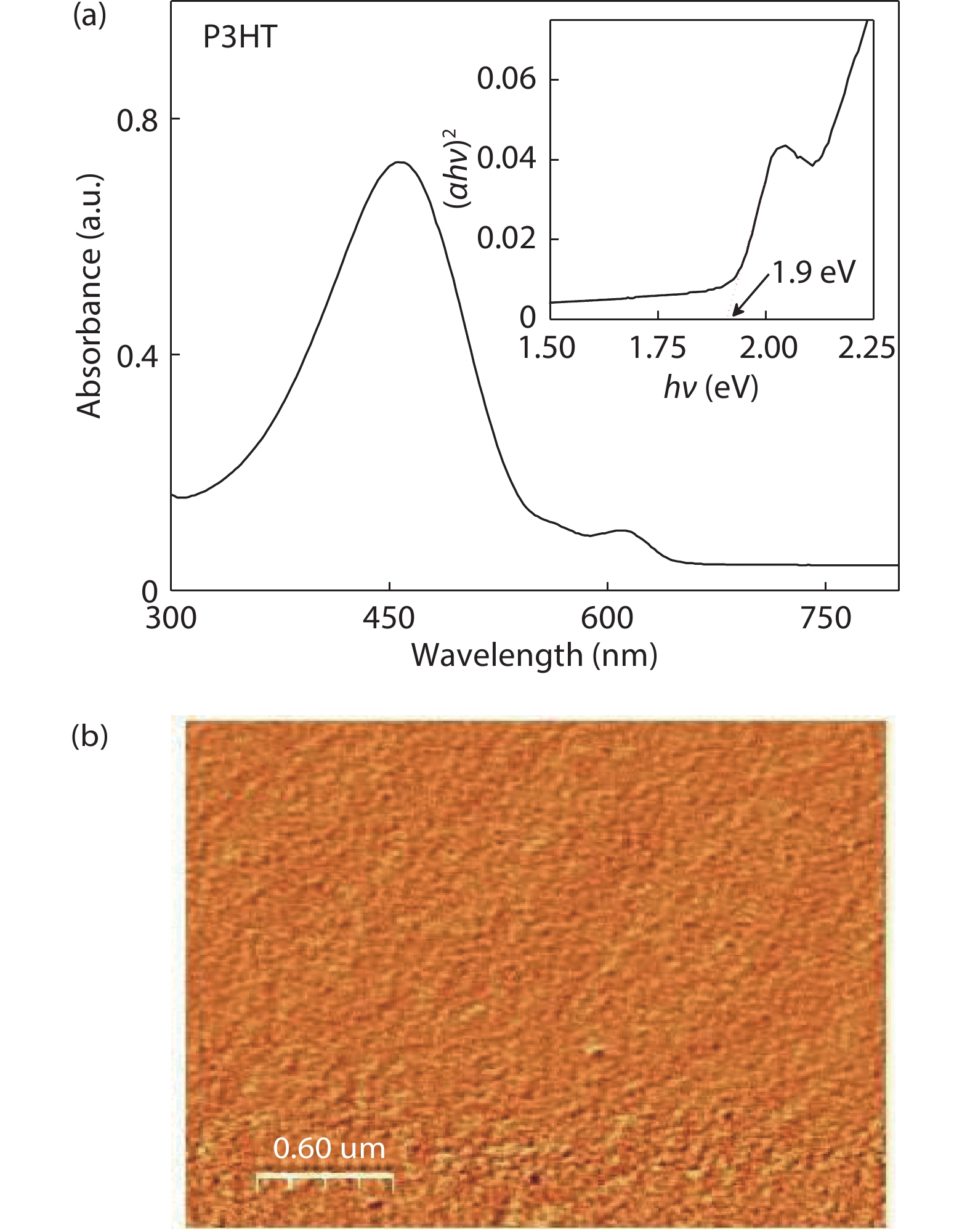
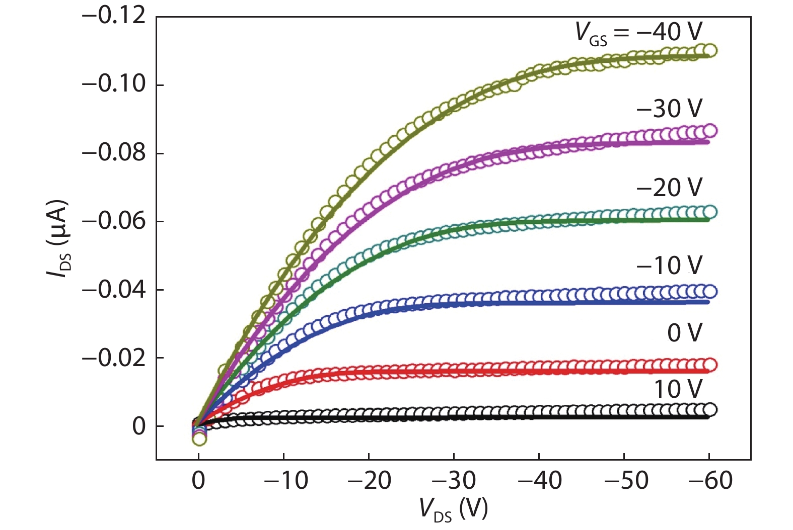


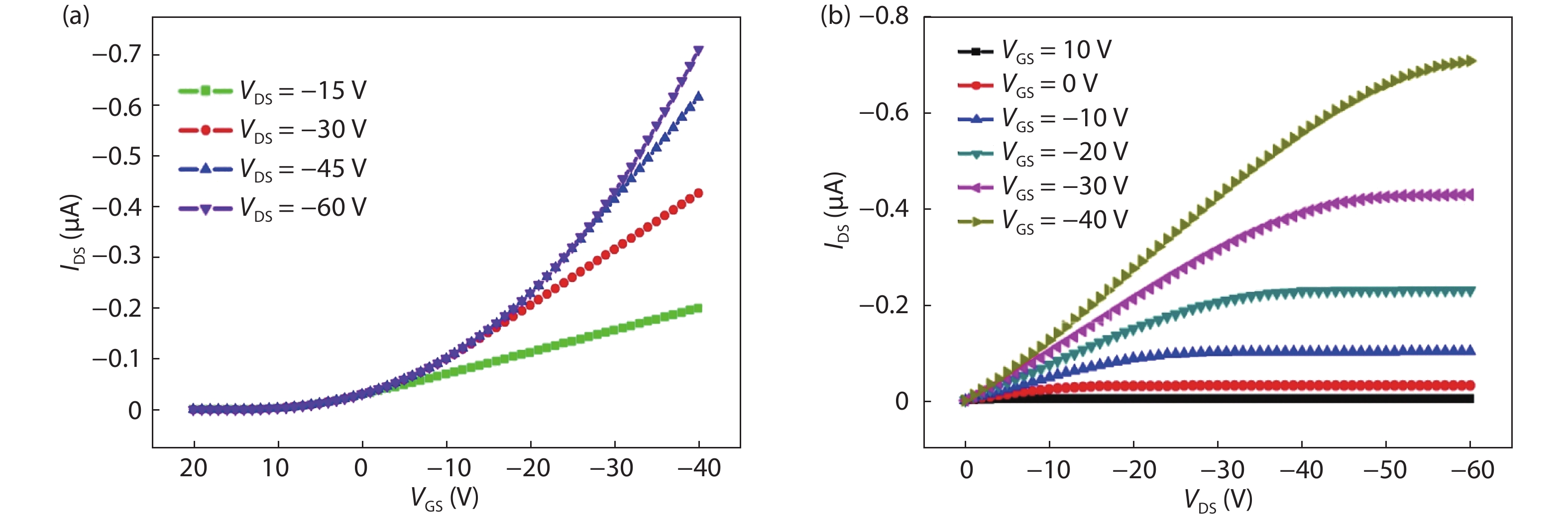
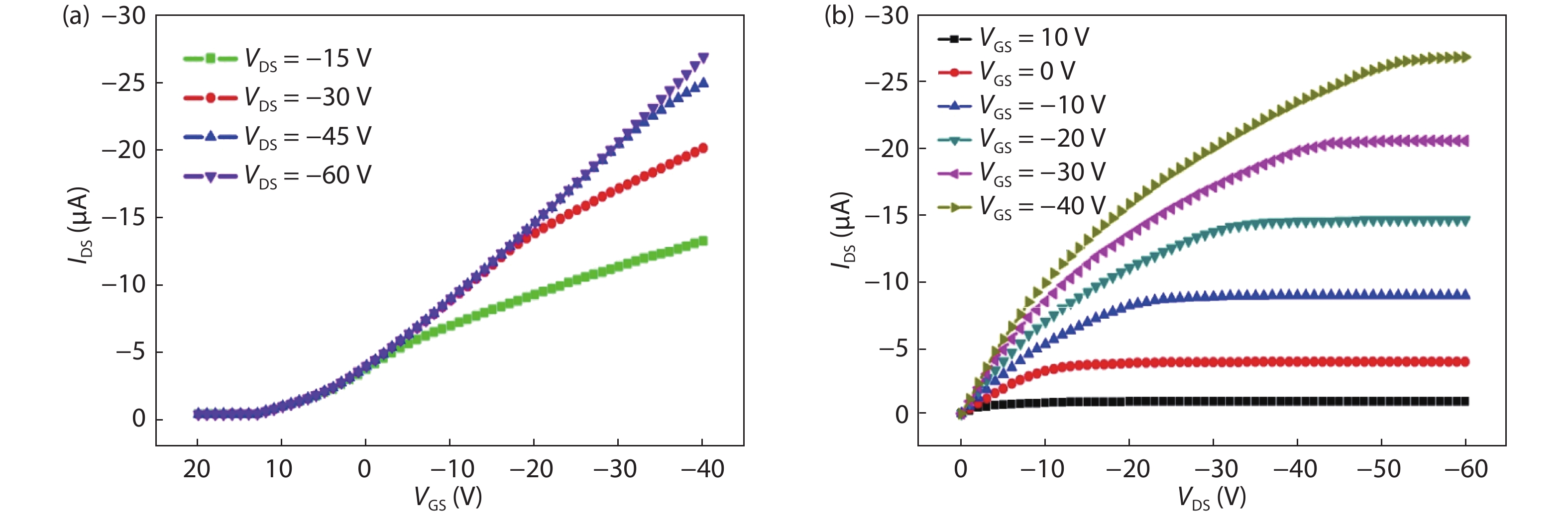

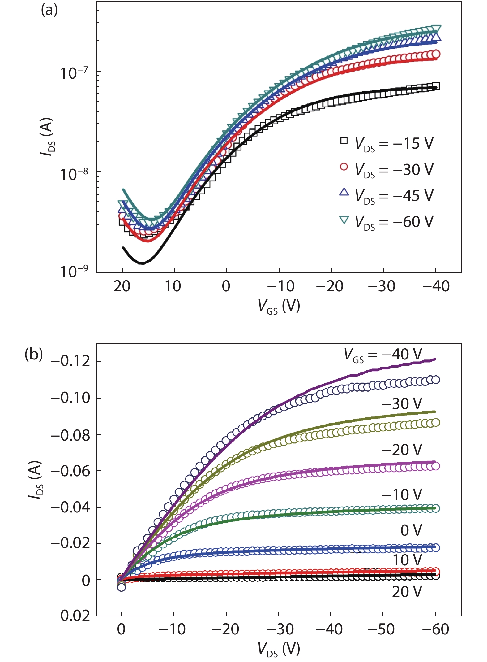

Table 1. Material parameters for P3HT.
| Parameter | Value |
| Effective density of states in the conduction band (Nc) | 2 × 1021 cm–3[17] |
| Effective density of states in the valance band (Nv) | 2 × 1021 cm–3[17] |
| Organic Semiconductor Dielectric constants (ε) | 3.0[17] |
| Energy gap at 300 K (Eg) | 1.9 eV (experimental value, see Fig. 2(a)) |
| Electron affinity (χ) | 3.5 eV[17] |
| Electron mobility (μn) | 1 × 10⁻⁴ cm2/(V·s) |
| Hole Mobility (μp) | 5 × 10⁻⁴ cm2/(V·s) |
| Acceptor concentration (NA) | 2 × 1017 cm–3[31] |
 DownLoad: CSV
Table 2. DOS parameter for P3HT-based OTFT.
| Parameter | Value |
| NTA | 1.0 × 1012 cm–3/eV |
| NTD | 1.0 × 1012 cm–3/eV |
| NGA | 1.0 × 1016 cm–3/eV |
| NGD | 1.0 × 1012 cm–3/eV |
| EGA | 0.5 eV |
| EGD | 0.7 eV |
| WTA | 0.5 eV |
| WTD | 0.7 eV |
| WGA | 0.4 eV |
| WGD | 0.1 eV |
DownLoad: CSV
Table 3. Double peak DOS parameter for P3HT.
| Parameter | Value |
| NIA | 1.0 × 1014 cm–3/eV |
| NA | 1.0 × 1015 cm–3/eV |
| NID | 1.0 × 1014 cm–3/eV |
| ND | 5.0 × 1014 cm–3/eV |
| EA | 0.5 eV |
| ED | 0.7 eV |
DownLoad: CSV
Table 4. Hopping mobility model parameters of P3HT.
| Parameter | Value |
| 1.6 | |
| 2.0 × 108 cm–1 | |
| 4.0 × 10¹¹ Hz | |
| 1.7 | |
| 9.0 × 108 cm–1 | |
| 1.0 × 10¹² Hz |
DownLoad: CSV
Table 5. Pool-Frenkel mobility model parameter for P3HT-based OTFT.
| Parameter | Value |
| 6.524 × 10⁻⁵ eV | |
| 1.243 × 10⁻² eV(cm/V)1/2 | |
| 1.545 × 10⁻⁵ (cm/V)1/2 | |
| 1.792 × 10⁻² eV | |
| 7.758 × 10⁻⁵ eV(cm/V)1/2 | |
| 1.807 × 10⁻⁵ (cm/V)1/2 | |
| Interface charge (Qf) | 1 × 1010 cm–2 |
DownLoad: CSV
Table 6. Performance parameters of simulated P3HT based OTFTs.
| Parameter | Simulated | Experimented |
| Cox (nF/cm2) | 11.5 | 10 |
| Vt (V) | 14 | 15 |
| Gm (S) | 1.48 × 10⁻⁹ | 1.61 × 10⁻⁹ |
| µlin (cm2/(V·s)) | 5.36 × 10⁻⁵ | 6.70 × 10⁻⁵ |
| µsat (cm2/(V·s)) | 5.20 × 10⁻⁴ | 1.85 × 10⁻⁴ |
| SS (V/dec) | 14.61 | 11.29 |
| Ion/Ioff | 103.52 | 84.69 |
DownLoad: CSV
Table 7. Performance parameters comparison of four structures of P3HT-based OTFT.
| Parameter | BGBC | BGTC | TGBC | TGTC |
| Vt (V) | 14 | 13 | 18 | 16 |
| Gm (S) | 1.49 × 10⁻⁹ | 2.60 × 10⁻⁹ | 2.90 ×10⁻⁷ | 3.10 × 10⁻⁶ |
| µlin (cm2/(V·s)) | 5.36 × 10⁻⁵ | 9.42 × 10⁻⁵ | 1.05 × 10⁻² | 1.12 × 10⁻¹ |
| µsat (cm2/(V·s)) | 5.20 × 10⁻⁴ | 1.53 × 10⁻³ | 2.19 ×10⁻² | 8.73 × 10⁻³ |
| SS (V/dec) | 14.61 | 6.3 | 2.52 | 2.29 |
| Ion/Ioff | 1.03 × 10² | 9.25 × 10² | 7.50 × 101 | 2.23 ×10² |
DownLoad: CSV
Table 8. Compact model parameters extracted for P3HT-based OTFT.
| Parameter | Symbol | Unit | Values |
| The thickness of gate insulator | ti | m | 300 × 10–9 |
| Relative dielectric permittivity of the insulator at gate | ϵr | – | 3.37 |
| Relative dielectric permittivity of the semiconductor | ϵsc | – | 3.0 |
| Zero bias threshold voltage | VT | V | 14.57 |
| Trap densitystates Characteristic voltage | V0 | V | 1.92 |
| Characteristic effective accumulation channelmobility | µeff | m2/(V·s) | 7.14 × 10⁻⁷ |
| Characteristic voltage of the effective mobility | Vacc | V | 9.05 |
| Saturation modulation parameter | a(T) | – | 3.25 |
| Output conductance parameter | 1/V | 0.0 | |
| Knee shape parameter | m | – | 0.20 |
| Power law mobility parameter | α | – | 0.99 |
| Leakage saturation current | IOL | A | 3.1 × 10⁻⁹ |
| Leakage current gate bias non-ideality factor | NGSL | – | 5.34 × 10⁻³ |
| Leakage current drain bias non-ideality factor | NDSL | – | 3.18 × 10⁻⁹ |
| The minimum bulk conductance | S | 1.20 × 10⁻¹² | |
| Contact Resistance | RS + RD | MΩ | 262.81 |
DownLoad: CSV
Table 9. Low and high logic states used in logic circuit simulation based on P3HT based OTFTs.
| –100 | 0 ‘Low’ | 0 | 1 ‘High’ |
| 0 | 1 ‘High’ | –100 | 0 ‘Low’ |
DownLoad: CSV
| [1] |
Guo X J, Xu Y, Ogier S, et al. Current status and opportunities of organic thin-film transistor technologies. IEEE Trans Electron Devices, 2017, 64, 1906 doi: 10.1109/TED.2017.2677086
|
| [2] |
Ding L, Zhao J Q, Huang Y K, et al. Flexible-blade coating of small molecule organic semiconductor for low voltage organic field effect transistor. IEEE Electron Device Lett, 2017, 38, 338 doi: 10.1109/LED.2017.2657651
|
| [3] |
Jeong J, Kim M, Lee S H, et al. Self-defined short channel formation with micromolded separator and inkjet-printed source/drain electrodes in OTFTs. IEEE Electron Device Lett, 2011, 32, 1758 doi: 10.1109/LED.2011.2169646
|
| [4] |
Kim S H, Lee S H, Kim Y G, et al. Ink-jet-printed organic thin-film transistors for low-voltage-driven CMOS circuits with solution-processed AlOx gate insulator. IEEE Electron Device Lett, 2013, 34, 307 doi: 10.1109/LED.2012.2228461
|
| [5] |
Marien H, Steyaert M S J, van Veenendaal E, et al. Analog building blocks for organic smart sensor systems in organic thin-film transistor technology on flexible plastic foil. IEEE J Solid-State Circuits, 2012, 47, 1712 doi: 10.1109/JSSC.2012.2191038
|
| [6] |
Scarpa G, Idzko A L, Münzer A, et al. Low-cost solution-processable organic thin-film transistors for (bio)sensing applications. 2011 IEEE Sensors, 2011, 1581
|
| [7] |
Mohamad K A, Alias A, Saad I, et al. All-polymer organic field-effect transistors with memory element. 2012 Third International Conference on Intelligent Systems Modelling and Simulation, 2012, 743
|
| [8] |
Xu M L, Guo S X, Xiang L Y, et al. High mobility flexible ferroelectric organic transistor nonvolatile memory with an ultrathin AlOx interfacial layer. IEEE Trans Electron Devices, 2018, 65, 1113 doi: 10.1109/TED.2018.2797936
|
| [9] |
Wang A, Kymissis I, Bulovic V, et al. Engineering density of semiconductor-dielectric interface states to modulate threshold voltage in OFETs. IEEE Trans Electron Devices, 2006, 53, 9 doi: 10.1109/TED.2005.860633
|
| [10] |
Ramos B, Lopes M, Buso D, et al. Performance enhancement in N-channel organic field-effect transistors using ferroelectric material as a gate dielectric. IEEE Trans Nanotechnol, 2017, 16, 773 doi: 10.1109/TNANO.2017.2683201
|
| [11] |
Feng L R, Zhao J Q, Tang W, et al. Solution processed organic thin-film transistors with hybrid low/high voltage operation. J Disp Technol, 2014, 10, 971 doi: 10.1109/JDT.2014.2344040
|
| [12] |
Mizukami M, Oku S, Cho S I, et al. A solution-processed organic thin-film transistor backplane for flexible multiphoton emission organic light-emitting diode displays. IEEE Electron Device Lett, 2015, 36, 841 doi: 10.1109/LED.2015.2443184
|
| [13] |
Takshi A, Dimopoulos A, Madden J D. Simulation of a low-voltage organic transistor compatible with printing methods. IEEE Trans Electron Devices, 2008, 55, 276 doi: 10.1109/TED.2007.910615
|
| [14] |
Jiménez Tejada J A, López Varo P, Cammidge A N, et al. Compact modeling of organic thin-film transistors with solution processed octadecyl substituted tetrabenzotriazaporphyrin as an active layer. IEEE Trans Electron Devices, 2017, 64, 2629 doi: 10.1109/TED.2017.2690976
|
| [15] |
Saini D, Saini S, Negi S. Modelling and comparison of single gate and dual gate organic thin film transistor. 2016 International Conference on Emerging Trends in Communication Technologies (ETCT), 2016, 1
|
| [16] |
TCAD Atlas User’s Manual, SILVACO® international, 2018
|
| [17] |
Dwivedi A D D, Dwivedi R D, Dwivedi R D, et al. Numerical simulation of P3HT based organic thin film transistors (OTFTs). Int J Microelectron Digit Integr Circuits, 2015, 1, 13
|
| [18] |
Tiwari S, Singh A K, Joshi L, et al. Poly-3-hexylthiophene based organic field-effect transistor: Detection of low concentration of ammonia. Sens Actuators B, 2012, 171/172, 962 doi: 10.1016/j.snb.2012.06.010
|
| [19] |
Ortiz-Conde A, Garcı́a Sánchez F J, Liou J J, et al. A review of recent MOSFET threshold voltage extraction methods. Microelectron Reliab, 2002, 42, 583 doi: 10.1016/S0026-2714(02)00027-6
|
| [20] |
Han C Y, Tang W M, Lai P T. High-mobility pentacene organic thin-film transistor with LaxNb1– xOy gate dielectric fabricated on vacuum tape. IEEE Trans Electron Devices, 2017, 64, 1716 doi: 10.1109/TED.2017.2661806
|
| [21] |
Singh S, Kumar M. Modeling of on-off current and cutoff frequency in organic thin film transistors. Int J Innov Technol Explor Eng, 2020, 9, 3028 doi: 10.35940/ijitee.C8063.019320
|
| [22] |
Vyas S, Dwivedi A D D, Dwivedi R D. Effect of gate dielectric on the performance of ZnO based thin film transistor. Superlattices Microstruct, 2018, 120, 223 doi: 10.1016/j.spmi.2018.05.040
|
| [23] |
Dwivedi A D D. Numerical simulation and spice modeling of organic thin film transistors (OTFTs). Int J Adv App Phy Res, 2014, 1, 14 doi: 10.15379/2408-977X.2014.01.02.3
|
| [24] |
Kumari P, Dwivedi A D D. Modeling and simulation of pentacene based organic thin film transistors with organic gate dielectrics. J Microelectron Solid State Devices, 2017, 4, 13 doi: 10.37591/jomsd.v4i3.275
|
| [25] |
Kushwah N S, Dwivedi A D D. Computer modeling of organic thin film transistors (OTFTs) using Verilog-A. J Microelectron Solid State Devices, 2018, 5, 1 doi: 10.37591/jomsd.v5i1.588
|
| [26] |
Kumari P, Dwivedi A D D. Numerical simulation and characteriation of pentacene based organic thin film transistors with top and bottom gate configurations. Global J Res Eng, 2019
|
| [27] |
Dwivedi A D D, Kumari P. TCAD simulation and performance analysis of single and dual gate OTFTs. Surf Rev Lett, 2020, 27, 1950145 doi: 10.1142/S0218625X19501452
|
| [28] |
Dwivedi A D D, Dhar Dwivedi R, Dhar Dwivedi R, et al. Simulation and compact modeling of organic thin film transistors (OTFTs) for circuit simulation. Int J Adv App Phy Res, 2019, 6, 1 doi: 10.15379/2408-977X.2019.06.01.01
|
| [29] |
Iñiguez B, Picos R, Veksler D, et al. Universal compact model for long- and short-channel thin-film transistors. Solid-State Electron, 2008, 52, 400 doi: 10.1016/j.sse.2007.10.027
|
| [30] |
Estrada M, Cerdeira A, Puigdollers J, et al. Accurate modeling and parameter extraction method for organic TFTs. Solid-State Electron, 2005, 49, 1009 doi: 10.1016/j.sse.2005.02.004
|
| [31] |
Dwivedi A D D, Jain S K, Dwivedi R D, et al. Numerical simulation and compact modeling of low voltage pentacene based OTFTs. J Sci: Adv Mater Devices, 2019, 4, 561 doi: 10.1016/j.jsamd.2019.10.006
|
| [32] |
UTMOST IV and Smart Spice models manual. Silvaco International, Santa Clara, CA, USA, 2018
|
| [33] |
Dwivedi A D D, Jain S K, Dwivedi R D, et al. Numerical simulation and compact modeling of thin film transistors for future flexible electronics. Hybrid Nanomater: Flexible Electron Mater, 2020
|
| [34] |
Chaudhary V, Kumar N, Singh A K. Solubility dependent trap density in poly (3-hexylthiophene) organic Schottky diodes at room temperature. Synth Met, 2019, 250, 88 doi: 10.1016/j.synthmet.2019.03.006
|
| [35] |
Chaudhary V, Pandey R K, Prakash R, et al. Self-assembled H-aggregation induced high performance poly (3-hexylthiophene) Schottky diode. J Appl Phys, 2017, 122, 225501 doi: 10.1063/1.4997554
|
| [36] |
De Vusser S, Genoe J, Heremans P. Influence of transistor parameters on the noise margin of organic digital circuits. IEEE Trans Electron Devices, 2006, 53, 601 doi: 10.1109/TED.2006.870876
|
| [37] |
Omar S, Mandal S, Ashok A, et al. Organic inverter: Theoretical analysis using load matching technique. Microelectron Reliab, 2011, 51, 2173 doi: 10.1016/j.microrel.2011.05.014
|
| [38] |
Huang T C, Fukuda K, Lo C M, et al. Pseudo-CMOS: A design style for low-cost and robust flexible electronics. IEEE Trans Electron Devices, 2011, 58, 141 doi: 10.1109/TED.2010.2088127
|
| [39] |
Jain S K, Dadhich S, Dwivedi A D D. Numerical simulation based comparative study of P3HT based top contact and bottom contact OTFTs. J Electron Des Technol, 2020, 10, 27 doi: 10.37591/joedt.v10i3.3390
|


Article views: 3336 Times PDF downloads: 112 Times Cited by: 0 Times
Received: 20 January 2021 Revised: 01 March 2021 Online: Accepted Manuscript: 21 April 2021Uncorrected proof: 25 April 2021Published: 05 July 2021
| Citation: |
Shubham Dadhich, A. D. D. Dwivedi, Arun Kumar Singh. Fabrication, characterization, numerical simulation and compact modeling of P3HT based organic thin film transistors[J]. Journal of Semiconductors, 2021, 42(7): 074102. doi: 10.1088/1674-4926/42/7/074102
S Dadhich, A D D Dwivedi, A K Singh, Fabrication, characterization, numerical simulation and compact modeling of P3HT based organic thin film transistors[J]. J. Semicond., 2021, 42(7): 074102. doi: 10.1088/1674-4926/42/7/074102.
Export: BibTex EndNote

|
| [1] |
Guo X J, Xu Y, Ogier S, et al. Current status and opportunities of organic thin-film transistor technologies. IEEE Trans Electron Devices, 2017, 64, 1906 doi: 10.1109/TED.2017.2677086
|
| [2] |
Ding L, Zhao J Q, Huang Y K, et al. Flexible-blade coating of small molecule organic semiconductor for low voltage organic field effect transistor. IEEE Electron Device Lett, 2017, 38, 338 doi: 10.1109/LED.2017.2657651
|
| [3] |
Jeong J, Kim M, Lee S H, et al. Self-defined short channel formation with micromolded separator and inkjet-printed source/drain electrodes in OTFTs. IEEE Electron Device Lett, 2011, 32, 1758 doi: 10.1109/LED.2011.2169646
|
| [4] |
Kim S H, Lee S H, Kim Y G, et al. Ink-jet-printed organic thin-film transistors for low-voltage-driven CMOS circuits with solution-processed AlOx gate insulator. IEEE Electron Device Lett, 2013, 34, 307 doi: 10.1109/LED.2012.2228461
|
| [5] |
Marien H, Steyaert M S J, van Veenendaal E, et al. Analog building blocks for organic smart sensor systems in organic thin-film transistor technology on flexible plastic foil. IEEE J Solid-State Circuits, 2012, 47, 1712 doi: 10.1109/JSSC.2012.2191038
|
| [6] |
Scarpa G, Idzko A L, Münzer A, et al. Low-cost solution-processable organic thin-film transistors for (bio)sensing applications. 2011 IEEE Sensors, 2011, 1581
|
| [7] |
Mohamad K A, Alias A, Saad I, et al. All-polymer organic field-effect transistors with memory element. 2012 Third International Conference on Intelligent Systems Modelling and Simulation, 2012, 743
|
| [8] |
Xu M L, Guo S X, Xiang L Y, et al. High mobility flexible ferroelectric organic transistor nonvolatile memory with an ultrathin AlOx interfacial layer. IEEE Trans Electron Devices, 2018, 65, 1113 doi: 10.1109/TED.2018.2797936
|
| [9] |
Wang A, Kymissis I, Bulovic V, et al. Engineering density of semiconductor-dielectric interface states to modulate threshold voltage in OFETs. IEEE Trans Electron Devices, 2006, 53, 9 doi: 10.1109/TED.2005.860633
|
| [10] |
Ramos B, Lopes M, Buso D, et al. Performance enhancement in N-channel organic field-effect transistors using ferroelectric material as a gate dielectric. IEEE Trans Nanotechnol, 2017, 16, 773 doi: 10.1109/TNANO.2017.2683201
|
| [11] |
Feng L R, Zhao J Q, Tang W, et al. Solution processed organic thin-film transistors with hybrid low/high voltage operation. J Disp Technol, 2014, 10, 971 doi: 10.1109/JDT.2014.2344040
|
| [12] |
Mizukami M, Oku S, Cho S I, et al. A solution-processed organic thin-film transistor backplane for flexible multiphoton emission organic light-emitting diode displays. IEEE Electron Device Lett, 2015, 36, 841 doi: 10.1109/LED.2015.2443184
|
| [13] |
Takshi A, Dimopoulos A, Madden J D. Simulation of a low-voltage organic transistor compatible with printing methods. IEEE Trans Electron Devices, 2008, 55, 276 doi: 10.1109/TED.2007.910615
|
| [14] |
Jiménez Tejada J A, López Varo P, Cammidge A N, et al. Compact modeling of organic thin-film transistors with solution processed octadecyl substituted tetrabenzotriazaporphyrin as an active layer. IEEE Trans Electron Devices, 2017, 64, 2629 doi: 10.1109/TED.2017.2690976
|
| [15] |
Saini D, Saini S, Negi S. Modelling and comparison of single gate and dual gate organic thin film transistor. 2016 International Conference on Emerging Trends in Communication Technologies (ETCT), 2016, 1
|
| [16] |
TCAD Atlas User’s Manual, SILVACO® international, 2018
|
| [17] |
Dwivedi A D D, Dwivedi R D, Dwivedi R D, et al. Numerical simulation of P3HT based organic thin film transistors (OTFTs). Int J Microelectron Digit Integr Circuits, 2015, 1, 13
|
| [18] |
Tiwari S, Singh A K, Joshi L, et al. Poly-3-hexylthiophene based organic field-effect transistor: Detection of low concentration of ammonia. Sens Actuators B, 2012, 171/172, 962 doi: 10.1016/j.snb.2012.06.010
|
| [19] |
Ortiz-Conde A, Garcı́a Sánchez F J, Liou J J, et al. A review of recent MOSFET threshold voltage extraction methods. Microelectron Reliab, 2002, 42, 583 doi: 10.1016/S0026-2714(02)00027-6
|
| [20] |
Han C Y, Tang W M, Lai P T. High-mobility pentacene organic thin-film transistor with LaxNb1– xOy gate dielectric fabricated on vacuum tape. IEEE Trans Electron Devices, 2017, 64, 1716 doi: 10.1109/TED.2017.2661806
|
| [21] |
Singh S, Kumar M. Modeling of on-off current and cutoff frequency in organic thin film transistors. Int J Innov Technol Explor Eng, 2020, 9, 3028 doi: 10.35940/ijitee.C8063.019320
|
| [22] |
Vyas S, Dwivedi A D D, Dwivedi R D. Effect of gate dielectric on the performance of ZnO based thin film transistor. Superlattices Microstruct, 2018, 120, 223 doi: 10.1016/j.spmi.2018.05.040
|
| [23] |
Dwivedi A D D. Numerical simulation and spice modeling of organic thin film transistors (OTFTs). Int J Adv App Phy Res, 2014, 1, 14 doi: 10.15379/2408-977X.2014.01.02.3
|
| [24] |
Kumari P, Dwivedi A D D. Modeling and simulation of pentacene based organic thin film transistors with organic gate dielectrics. J Microelectron Solid State Devices, 2017, 4, 13 doi: 10.37591/jomsd.v4i3.275
|
| [25] |
Kushwah N S, Dwivedi A D D. Computer modeling of organic thin film transistors (OTFTs) using Verilog-A. J Microelectron Solid State Devices, 2018, 5, 1 doi: 10.37591/jomsd.v5i1.588
|
| [26] |
Kumari P, Dwivedi A D D. Numerical simulation and characteriation of pentacene based organic thin film transistors with top and bottom gate configurations. Global J Res Eng, 2019
|
| [27] |
Dwivedi A D D, Kumari P. TCAD simulation and performance analysis of single and dual gate OTFTs. Surf Rev Lett, 2020, 27, 1950145 doi: 10.1142/S0218625X19501452
|
| [28] |
Dwivedi A D D, Dhar Dwivedi R, Dhar Dwivedi R, et al. Simulation and compact modeling of organic thin film transistors (OTFTs) for circuit simulation. Int J Adv App Phy Res, 2019, 6, 1 doi: 10.15379/2408-977X.2019.06.01.01
|
| [29] |
Iñiguez B, Picos R, Veksler D, et al. Universal compact model for long- and short-channel thin-film transistors. Solid-State Electron, 2008, 52, 400 doi: 10.1016/j.sse.2007.10.027
|
| [30] |
Estrada M, Cerdeira A, Puigdollers J, et al. Accurate modeling and parameter extraction method for organic TFTs. Solid-State Electron, 2005, 49, 1009 doi: 10.1016/j.sse.2005.02.004
|
| [31] |
Dwivedi A D D, Jain S K, Dwivedi R D, et al. Numerical simulation and compact modeling of low voltage pentacene based OTFTs. J Sci: Adv Mater Devices, 2019, 4, 561 doi: 10.1016/j.jsamd.2019.10.006
|
| [32] |
UTMOST IV and Smart Spice models manual. Silvaco International, Santa Clara, CA, USA, 2018
|
| [33] |
Dwivedi A D D, Jain S K, Dwivedi R D, et al. Numerical simulation and compact modeling of thin film transistors for future flexible electronics. Hybrid Nanomater: Flexible Electron Mater, 2020
|
| [34] |
Chaudhary V, Kumar N, Singh A K. Solubility dependent trap density in poly (3-hexylthiophene) organic Schottky diodes at room temperature. Synth Met, 2019, 250, 88 doi: 10.1016/j.synthmet.2019.03.006
|
| [35] |
Chaudhary V, Pandey R K, Prakash R, et al. Self-assembled H-aggregation induced high performance poly (3-hexylthiophene) Schottky diode. J Appl Phys, 2017, 122, 225501 doi: 10.1063/1.4997554
|
| [36] |
De Vusser S, Genoe J, Heremans P. Influence of transistor parameters on the noise margin of organic digital circuits. IEEE Trans Electron Devices, 2006, 53, 601 doi: 10.1109/TED.2006.870876
|
| [37] |
Omar S, Mandal S, Ashok A, et al. Organic inverter: Theoretical analysis using load matching technique. Microelectron Reliab, 2011, 51, 2173 doi: 10.1016/j.microrel.2011.05.014
|
| [38] |
Huang T C, Fukuda K, Lo C M, et al. Pseudo-CMOS: A design style for low-cost and robust flexible electronics. IEEE Trans Electron Devices, 2011, 58, 141 doi: 10.1109/TED.2010.2088127
|
| [39] |
Jain S K, Dadhich S, Dwivedi A D D. Numerical simulation based comparative study of P3HT based top contact and bottom contact OTFTs. J Electron Des Technol, 2020, 10, 27 doi: 10.37591/joedt.v10i3.3390
|

 WeChat ID
Journal of Semiconductors © 2017 All Rights Reserved 京ICP备05085259号-2